1. Introduction
Since the report of room temperature photoluminescence in porous silicon (PS) [
1], this material has been extensively investigated for the development of optoelectronic devices. PS is constituted by a nanocrystalline skeleton (quantum sponge) immersed in a network of pores and can be obtained simply by electrochemical etching of silicon in aqueous hydrofluoric (HF) [
2,
3]. Due to its many special characteristics such as extremely large surface-area-to-volume ratio, modulated energy bandgap, absorption spectrum within the solar irradiation, surface roughening with low reflection losses, and high photoconductivity, PS is very suitable for applications in photovoltaic devices [
4]. In particular, PS structures have been intensively introduced in the device design of solar cells to increase the cell’s conversion efficiency [
5,
6,
7]. In most of the related research, PS films acted as the surface texturing and anti-reflection (AR) layers to reduce the light-reflection losses or as the surface passivation layers to decrease surface carrier recombination velocity. On the other hand, PS can potentially serve as the parts of the active layer to effectively generate photo-induced carriers because of its wide energy bandgap and high photoconduction in response to solar irradiation [
8,
9]. However, a primary drawback of PS for use of the light-absorption layer in a photovoltaic device is its comparatively narrow spectral photoresponses. Therefore, to get higher and broader spectral photoresponses within the spectrum of the solar irradiation is a primary requirement for the fabrication of efficient PS-based solar cells.
An important scheme to increase the light absorbance range of devices is using cell structures with multi-junctions (
i.e., the “tandem cell” structures). Tandem cells are solar cells with multiple
p–n junctions made of different semiconductor materials with different bandgap energy. Because each semiconductor material is sensitive to a different part of the solar spectrum, tandem cells can obtain enhanced overall sunlight photoresponses and achieve higher conversion efficiency. However, these tandem cells are usually not suitable for mass production of silicon (Si) solar cells since their fabrication processes are so complicated and are not Si-compatible [
10,
11].
A promising Si-based tandem-like structure is the PS multilayer (PSML) structure composed of stacked PS layers with different porosity. In the past, PSML had received much interest due to its tunable optical and electronic properties [
4]. Because the refractive index of PS can be tuned through the porosity using controlled electrochemical-etching conditions, PSML with modulated refractive index can be fabricated by stacking PS layers of different porosity. These PSML structures can be used to make optical filters, waveguides, resonating cavities and mirrors for device applications [
12,
13]. Most of the recent studies about applications of PSML in solar cells mainly focused at the optimization of AR coatings [
14,
15]. There are few reports on cells with light-absorption areas based on PSML structures. Since the optical bandgap of PS can be tuned by its porosity, it is feasible to broaden the photoresponse spectra of Si photovoltaic devices by use of multi-bandgap PSML structures. Based on the fact that a PS layer of higher porosity has higher bandgap energy, a PSML structure composed of triple stacking layers with high-, medium- and low-porosity (from top to bottom) will absorb the sun light in the short-, medium- and long-wavelength bands respectively. Such a “tandem-like” PSML structure can potentially harvest a broader range of the sun’s energy to make a Si-based solar cell more efficient.
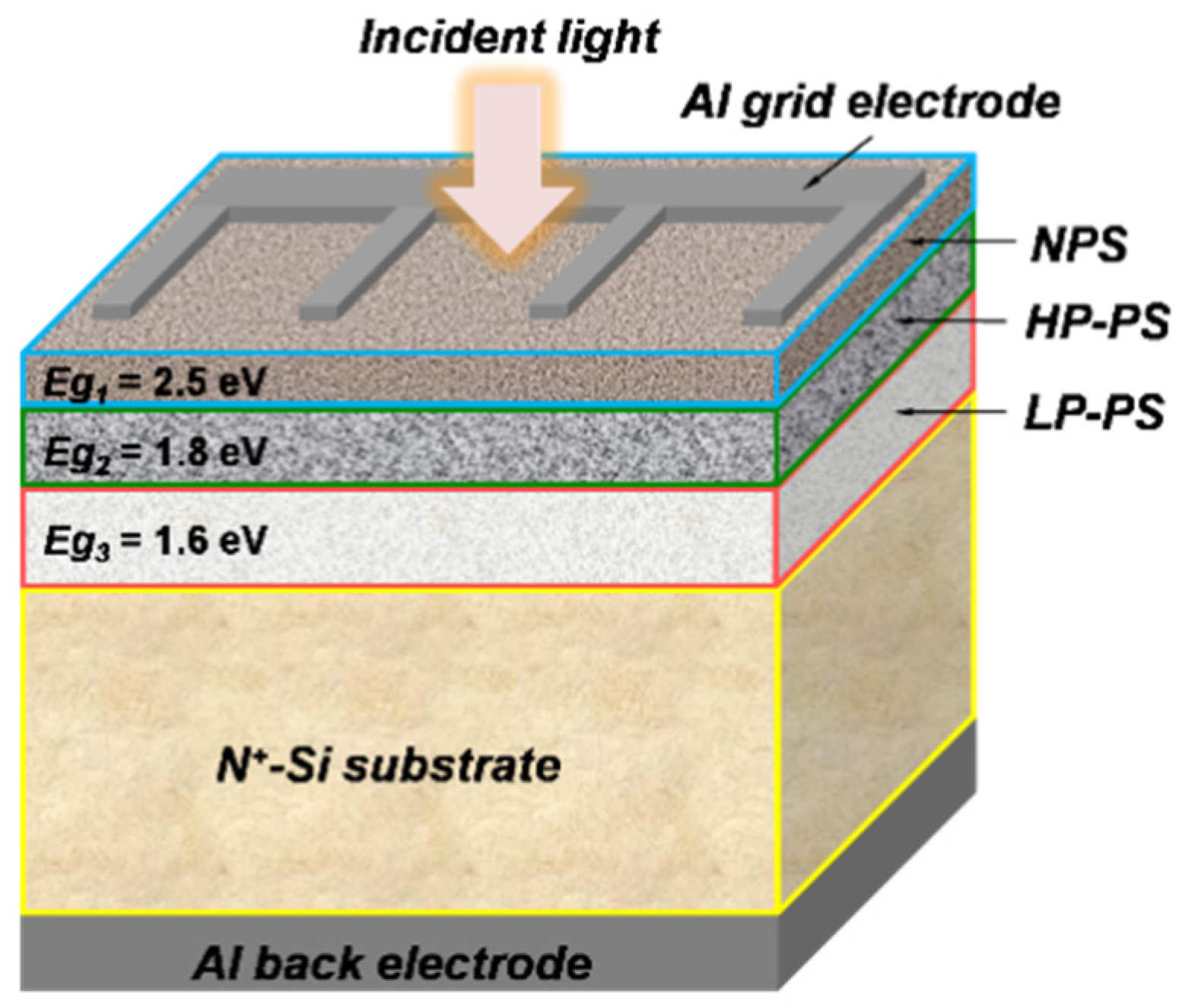
Utilization of PSML as the light-absorption region of a device will face a dilemma in choosing the porosity of the upmost PS layer. To absorb light of shorter wavelength, the upmost PS layer must be designed with higher porosity. However, a PS layer with higher porosity has higher resistance, lower hardness and higher density of defects [
4,
5]. Therefore, using a high-porosity PS surface layer will result in high series resistance and degradation of metal contacts. To solve this problem, we proposed a special nanoporous-Si (NPS) thin film for serving as the surface active layer. The NPS layer associated with two stacked PS layers of different porosity will construct a triple-layered PS (TLPS) structure with multiple bandgap energy. Such a TLPS structure can be produced on Si substrates by tuning the etching parameters in an electrochemical anodization process. In this paper, we report the preparation and characterization of TLPS structures and demonstrated the improvements on the spectral photoresponses and light-absorption capability of Si-based photovoltaic devices fabricated with the developed TLPS structures.
3. Results and Discussion
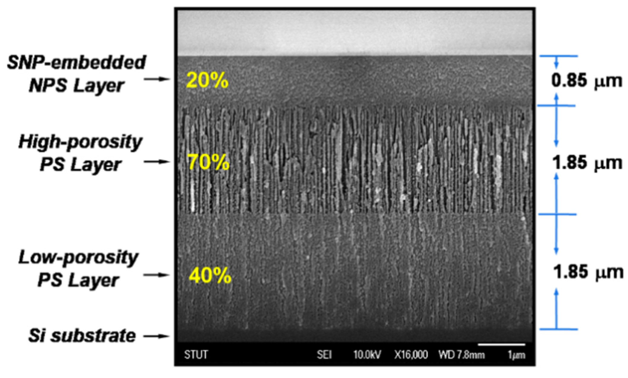
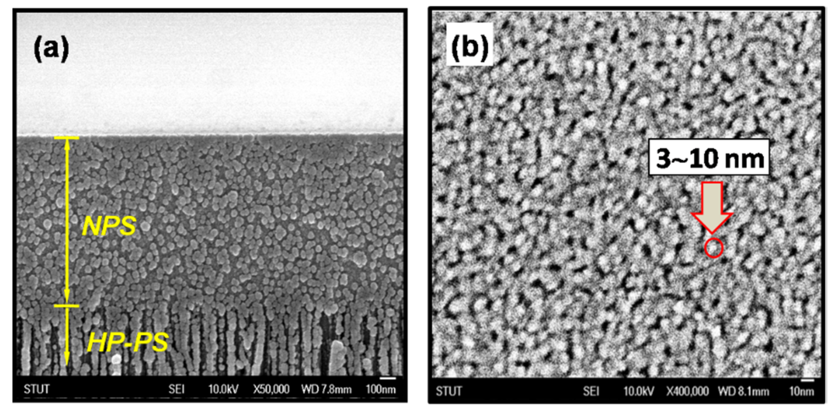
Figure 3a shows the zoom-in SEM photo-image of the prepared NPS layer in
Figure 1. It can be observed that the NPS layer has a special film-like structure, unlike the beneath HP-PS layer which has the common morphology of meso- or micro-PS layers generated from electrochemical-etching of Si wafers.
Figure 3b shows a high-magnification SEM image of the surface of the NPS film. As shown in this figure, the NPS film is embedded with uniformly distributed Si-nanocrystals and nano-sized holes. Average sizes of these Si-nanocrystals are estimated to be about 3–10 nm in diameters. According to the reports of Lee
et al. [
17], the bandgap energy of a PS material with quantum-sized Si-crystallites of 3 nm is about 2.5 eV. This value is close to that was predicted by Suemune
et al. [
18] and conforms to the
Egopt value of the NPS film measured from the Tauc’s plots in this work. The
Egopt of the beneath HP-PS layer with porosity of 70% and the LP-PS layer with porosity of 30% got from the Tauc’s plots is about 1.8 eV and 1.6 eV, respectively. These values are consistent with those obtained from the optical absorption measurements in other studies [
17].
Figure 3.
(
a) The zoom-in SEM photo-image of the prepared NPS layer shown in
Figure 1; (
b) A high-magnification SEM image of the surface of the prepared NPS film.
Figure 3.
(
a) The zoom-in SEM photo-image of the prepared NPS layer shown in
Figure 1; (
b) A high-magnification SEM image of the surface of the prepared NPS film.
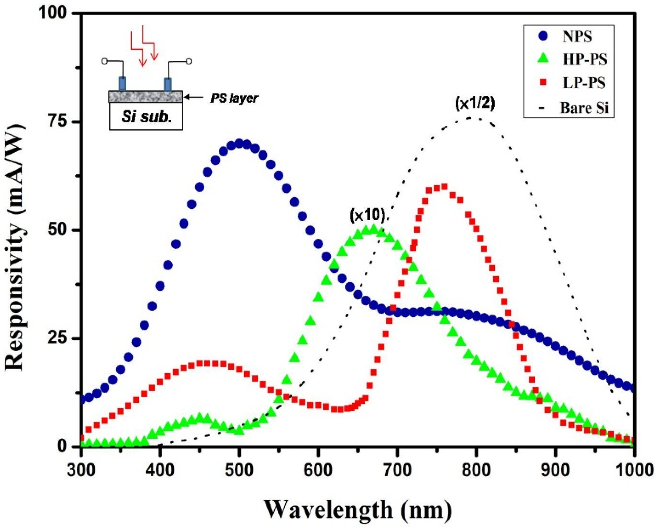
Figure 4 shows the spectral photoresponses of the individual PS (including NPS, HP-PS and LP-PS) layer prepared on a Si substrate. The photoresponses were measured with a TRIAX-320 spectrometer (HORIBA, Kyoto, Japan). To exclude as much as possible the influence of light absorption in the Si substrate, the responsivity was measured by using planar electrodes formed on the surface of the PS layer, as indicated in the inserted drawing. For comparison purposes, photoresponses of the bare Si substrate are also shown in the figure. As shown in the figure, the photoresponses of the LP-PS layer mainly appear within the ranges of wavelength between 650 nm and 850 nm, which corresponds to the optical band from red to infra-red (IR), and has a maximum responsivity of 62 mA/cm
2 at 750 nm. The LP-PS layer displays the common photoresponsive characteristics of a PS material, which has a narrower and blue-shifted response spectrum with smaller responsivity as compared to that of the bare Si. The responses of the HP-PS device shift further toward the band of shorter-wavelength between 550 nm (green) and 700 nm (red) with a much small peak responsivity of 5 mA/cm
2 at 670 nm. We thought the change in the region of the spectral responses is due to the higher porosity of layers which result in a larger
Egopt. The low responsivity is ascribed to not only its high resistivity and the high defect density, but also the large amount of the surface states and the high metal-contact resistance. By improving the metal contacts and the surface passivation on the PS layer, the responsivity of high-porosity PS can be largely enhanced [
19,
20]. Particularly in this work, the HP-PS layer was made under the NPS surface layer in the fabricated TLPS-based device. As a result, the surface of the HP-PS is effectively passivated by the NPS layer and the quality of metal-contact is thus not degraded by the HP-PS layer since the electrodes are formed on the NPS layer that has a surface with better quality. Therefore, the actual photoresponsivity of such a middle HP-PS layer in the TLPS structure is expected to be higher than that of an individual HP-PS layer as a surface layer on a Si substrate.
Figure 4.
The spectral photoresponses of the individual PS (NPS, HP-PS or LP-PS) layer prepared on a Si substrate, measured with planar electrodes on the PS surface as indicated in the inserted drawing. For comparison purposes, the measured data of the bare Si substrate are also shown.
Figure 4.
The spectral photoresponses of the individual PS (NPS, HP-PS or LP-PS) layer prepared on a Si substrate, measured with planar electrodes on the PS surface as indicated in the inserted drawing. For comparison purposes, the measured data of the bare Si substrate are also shown.
As shown in
Figure 4, the NPS layer not only exhibits much higher short-wavelength responses within 400–600 nm in the blue band (with a maximum responsivity of 72 mA/cm
2 at 500 nm), but also has apparent responses in the band of red-to-IR. It is supposed that the greatly enhanced blue-shifted responses come from the SNP’s embedded in the NPS films, which has
Egopt larger than 2 eV due to the quantum-size effects. The red-to-IR responses are ascribed to the light absorption in the micro-sized Si crystals around the SNP’s and the beneath Si substrate. Besides, it is interesting to find that the value of the peak responsivity of the NPS, HP-PS, and LP-PS layer corresponds respectively to a photon energy of 2.48 eV, 1.77 eV, and 1.65 eV, which is close to the value of
Egopt of the single PS layer respectively. This fact indicates that the
Egopt of a PS layer has significant influences on its photoresponses.
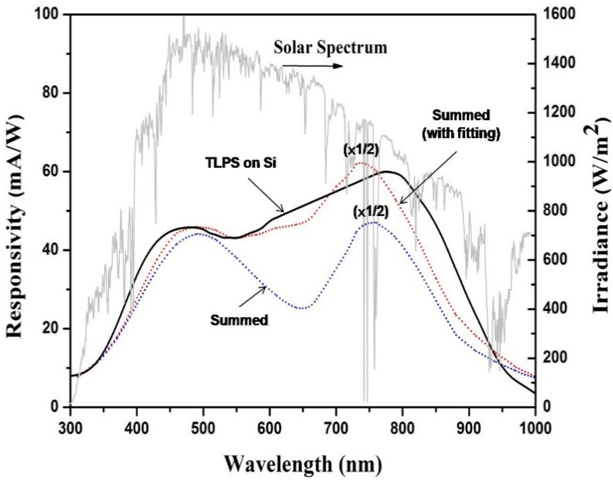
Figure 5 illustrates the spectral photoresponses of the photovoltaic devices with a TLPS structure on a Si substrate.
Figure 5.
The spectral photoresponses of the developed photovoltaic devices based on the TLPS structure and the individual PS (NPS, HP-PS or LP-PS) layer. The summed data (blue dotted line) were obtained by directly summing the three individual responses of the PS layer in
Figure 4, while the summed (with fitting) data (red dotted line) were obtained by using a 10-fold responses of HP-PS. The spectrum of solar irradiation is also shown in the figure for comparison purposes.
It is obvious that the TLPS-based device exhibits a broader photoresponse spectrum than that of an individual PS layer and the bare Si substrate. Most importantly, the developed device achieved a broadened and flat photoresponse spectrum that matches much more closely to that of the solar irradiance. That is a preferable property for development of highly efficient solar cell. From the spectral distribution of photoresponses of the three individual PS layer in
Figure 4, it is reasonable to suppose that the overall responses of a TLPS device are primarily composed of the generated responses in the three PS layers of a TLPS structure. To verify this assumption, we plotted the summed responses (denoted as “Summed”) that were obtained by directly summing the three individual responses of the PS layer in
Figure 4. The shown responses from the summed data were scaled down twofold for curve fitting, based on the fact that the resistance of the individual PS layer is smaller than that of a TLPS. It is apparent that the summed response spectra bend down between 550 nm and 750 nm as a result of the relatively small values of the individual HP-PS layer. However, the HP-PS is expected to exhibit higher responses as a middle layer in the TLPS structure due to the passivation of the NPS layer. By using a 10-fold response of HP-PS for summing, the plotted summed response spectra (denoted as “Summed (with fitting)”) become much flatter and more fitting to that of a TLPS-based device. These results support the expectation that the middle HP-PS layer can generate higher photoresponses than those of a surface HP-PS layer and indicate the assumption that the measured wide-band photoresponses come from a synergistic function of the three PS layers in the TLPS structure is valid.
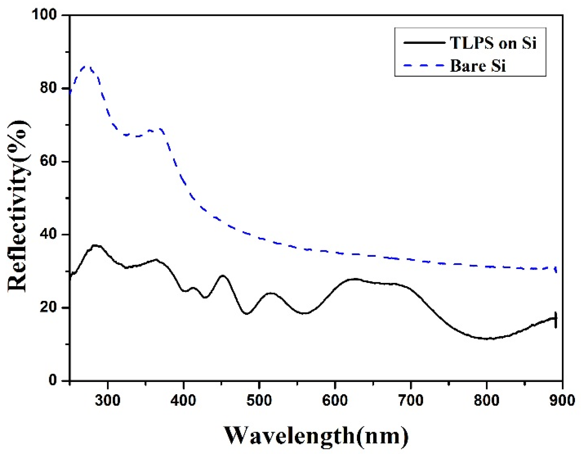
Furthermore, to check whether the multilayered PS structure on top of the Si substrate causes an interference effect on the photoresponses of the TLPS device, the spectral reflectance of the TLPS on a Si substrate was measured and shown in
Figure 6. From this figure, we can find that the average reflectivity of samples with TLPS on Si is about two times lower than that of the bare Si substrate in the visible band. That verifies the TLPS structure enhanced the light absorption. There are no obvious interference patterns appearing in the spectral reflectance. It indicates that the layered structure of TLPS in this work has a negligible interference effect on the generation of the spectral responses. Therefore, the improved spectral responses of the TLPS-based device are mainly owing to the multi-bandgap TLPS structures in which different layers with different
Egopt absorb different portions of the incident light and contribute all together to the whole photoresponses.
Figure 6.
The spectral reflectance of the TLPS structure on a Si substrate and the bare Si substrate.
Figure 6.
The spectral reflectance of the TLPS structure on a Si substrate and the bare Si substrate.
In a tandem cell, layers with different bandgap are stacked on top of one another with the highest bandgap layer upmost. Since layers with higher bandgap will absorb light of shorter wavelength, the device’s conversion efficiency can be largely increased if bandgap energy of each layer is optimally chosen. According to related researches, light-absorption spectra of PS with higher porosity usually shift towards shorter wavelength because of the larger bandgap energy of PS [
21]. These results accorded with the experimental ones in this work. In other words, PS layers with larger bandgap energy would absorb light of shorter wavelength. For the developed TLPS devices, the
Egopt value of each layer (from surface to the interior) in the light-absorption zone was 2.5 eV (NPS), 1.8 eV (HP-PS), 1.6 eV (LP-PS) and 1.1 eV (bulk Si), respectively. Since these
Egopt values spanned the main ranges of photon energy in the solar spectrum, the TLPS devices exhibited broadband photoresponses and were able to harvest more solar energy.
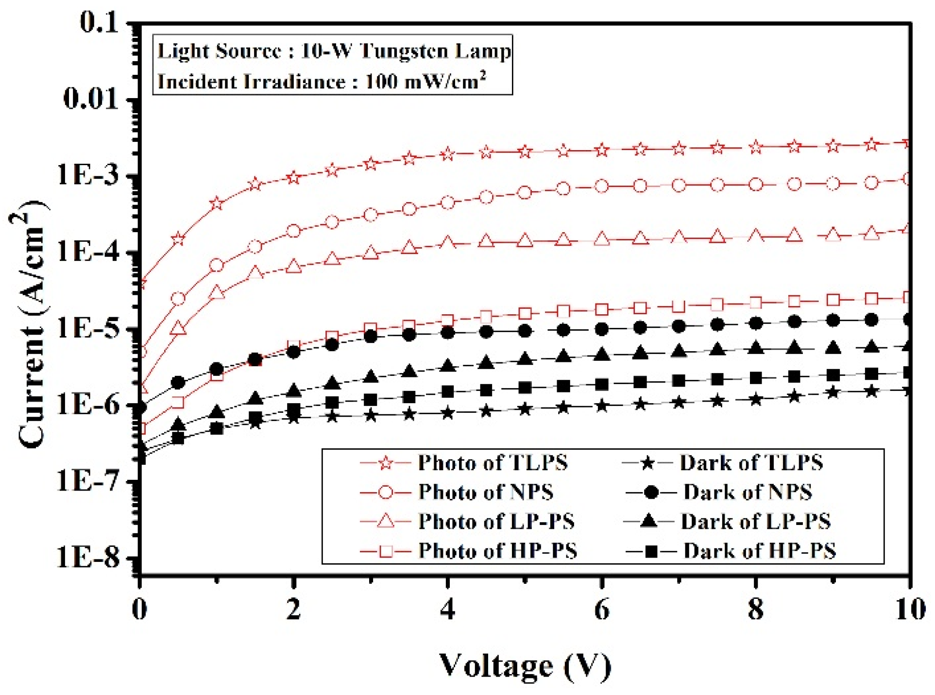
To assess the influences of the improved photoresponses on the performance of the photovoltaic devices, photo- and dark current-voltage characteristics of a TLPS-based device were measured and plotted in
Figure 7. For comparison purposes, similar devices based on a single PS (NPS, LP-PS or HP-PS) layer with a comparable thickness of about 4.5 μm were also fabricated and measured. The photocurrent of devices was measured under an incident irradiation of 100 mW/cm
2 by using a 10-W tungsten lamp with emitting light of wavelength ranging from 300 nm to 1100 nm and a peak wavelength of 550 nm. The reason for choosing such a tungsten lamp as the light source is that it has an irradiation spectrum similar to that of the sun. As observed in the figure, the TLPS-based device obtains the largest photocurrent and smallest dark current among these fabricated devices, indicating it has the most significant photoconduction property. Because the photoresponse spectrum of a TLPS device matched much more closely to that of the incident light, the higher photocurrent is mainly attributed to its better light-absorption ability coming from its improved photoresponses. The increase in the photocurrent indicates higher short-circuit current and higher conversion efficiency will be obtained by application of the TLPS structures. At a reverse bias of 5 V, the TLPS device has about one-order higher photocurrent than that of one based on a single LP-PS layer with porosity of 40%, which was applied as the surface film in a Si-based solar cell to achieve optimum device performance [
8]. That imply that the TLPS structures have good potential to improve the performance of a Si-based photovoltaic device.
Figure 7.
Photo and dark current-voltage (I–V) characteristics of photovoltaic devices based on the TLPS structures and the individual PS (NPS, LP-PS or HP-PS) layer on a Si substrate.
Figure 7.
Photo and dark current-voltage (I–V) characteristics of photovoltaic devices based on the TLPS structures and the individual PS (NPS, LP-PS or HP-PS) layer on a Si substrate.
The photocurrent of an NPS-based device is about half of that of the TLPS one at 5 V. From this data and the photoresponses of the individual NPS layer shown in
Figure 4, we deduced that the NPS layer contributes the most part of the photo-induced current to a TLPS device. In fact, there are many advantages by incorporating the NPS layer as the surface layer in the device. First, the NPS layer significantly increases the responses in the short-wavelength ranges around 450–550 nm that are just the portions including the maximum irradiance of the incident light (or the sun light), as we can observed in
Figure 4 and
Figure 5. Second, the micro-holes in the NPS layer provide a textured surface structure to reduce the light-reflection losses and augment the light absorption of devices. Third, as mentioned above, the NPS layer effectively passivates the lower HP-PS layer for complementing the middle-band photorespnses. Four, the smooth and dense surface of the NPS layer ensures the formation of a Schottky contact with high quality between the metal electrodes and the PS layer. This advantage can be realized from the comparison of the measured dark current between the TLPS and the HP-PS devices. Although a HP-PS device has larger series resistance than that of a TLPS device, it has higher dark current as shown in
Figure 7. For a Schottky device, high density of defects at the metal-semiconductor (M-S) interface will reduce the Schottky barrier of the M-S junction, thus causing a decrease in the photocurrent and increase in the reverse (or leakage) current [
22]. In a photovoltaic device, the leakage current dominates the dark current. That is, a PS-based photovoltaic device with a surface PS layer of higher-porosity usually had lower photocurrent and higher dark current due to the degraded Schottky contact. Therefore, the large amount of defects on the surface HP-PS layer cause high dark current. On the contrary, due to the incorporation of an NPS surface layer, the TLPS device with a middle HP-PS layer has a good Schottky contact to generate a higher photocurrent and retain lower dark current. Since the photo-to-dark current ratio (PDCR) is an important figure of merit for the performance of a photovoltaic device, the large PDCR of the fabricated TLPS-based device demonstrates that the multi-bandgapped PS structure has high potential in development of Si-based photovoltaic device.


