This section shows the results and discussion of the two circuit structure. The first section analyzes structure without a source line (SL) case and the second section analyzes structure with an SL case. As a result of the analysis, the sensing margin is improved by approximately 60% in the second case compared to the first case.
3.1. Simulation without SL
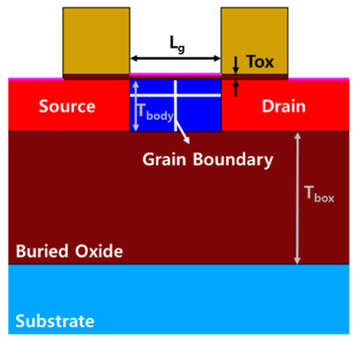
Figure 3 shows the array structure used in the first simulation. It consists of a cell for storing data, a WL connecting each gate terminal of transistors to each other, and a BL connecting each drain terminal of transistors to each other so that the same line shares the applied voltage. The selected cell in this study was a (3, 3) cell. The bias conditions used and the corresponding pulse timing diagrams are summarized and shown in
Table 2 and
Figure 4, respectively. The sample timing diagram presented in
Figure 4 is expressed only for the “1”-“0” case and “0”-“1”. For removing the remaining trapped holes at the GB, in all of the simulation cases, we initially wrote “0” on all cells before the first write.
Figure 4a shows the pulses applied to the selected line, that is, the pulses applied to BL3 and WL3.
Figure 4b shows the pulses applied to the unselected line, that is, to BL1, BL2, WL1, and WL2, except for the BL3 and WL3. Although not shown in
Figure 4, the hold operation is performed once before and after each write and read operation.
Figure 5 shows the voltages applied at each cell location depending on the data written to the selected cell. Because the voltage line shared with the selected cell is different for each cell, the applied voltage is different as well. For this reason, it can be expected that the disturbance will differ depending on the cell location.
Figure 6 shows an example of disturbance in simulation. The “0”-“1” case is illustrated, and the figure shows the read current depending on the cell location. The solid and dotted lines indicate the read current of the “1” and “0” states, respectively. As illustrated in
Figure 5, the three dotted lines represent different current levels owing to different degrees of disturbance. As such, in each of the four cases, only the cell with the greatest disturbance is selected and compared for measuring the sensing margin of the circuit. This means that the “0” and “1” state cells with the highest “0” current and the lowest “1” current, respectively, are selected. The sensing margin is calculated as the difference between the lowest value of “1” current and the highest value of “0” current among the four cases. The current values used to calculate the sensing margin are the values at 10 ns after application of the read voltage.
Figure 7a shows the read current of the cell with the largest disturbance in each of the cases. No symbol, circle symbol, and square symbol indicate the read currents of the data written to a single cell, largest disturbance among the “0” current cases, and largest disturbance among the “1” current cases, respectively. As depicted in
Figure 5, in the “0”-“0” case, the “0” current disturbance of the shared BL cell is the largest owing to the BTBT on the drain side and the migration of trapped electrons due to the source–drain voltage difference (V
ds). In the “0”-“1” case, the “0” current disturbance of the shared WL cell is the largest due to the BTBT on both the drain and source sides. In the “1”-“1” case, the “1” current disturbance of the shared BL cell is the largest because the trapped holes are removed upon the application of V
ds. Finally, in the “1”-“0” case, there are no disturbances in any cell; therefore, the shared BL cell with the least improvement is selected.
Figure 7b shows the read currents selected for calculating the sensing margin.
Table 3 lists the drain current values measured at 10 ns after application of the read voltage and the calculated sensing margin values. Considering that the minimum sensing margin for distinguishing whether a data point is 0 or 1 in the circuit is 3 µA, the simulated array structure satisfies the minimum sensing margin condition, meaning that it can be used as a memory device [
16].
3.2. Simulation with SL
Although the sensing margin of 6.86 µA exceeds the minimum sensing margin threshold, stable operation of the previously proposed circuit is not possible with variables such as continuous disturbance or long hold time. Therefore, the sensing margin must be improved to realize stable circuit operation. To this end, increasing the “1” current is more effective than the decreasing the “0” current by controlling V
ds. The “1” current is reinforced due to the occurrence of the BTBT on both the source and drain sides. To ensure the occurrence of the BTBT on the source side, 2 V is applied to source of the cell during the write “1” operation. Therefore, as shown in
Figure 8, the source line (SL) connecting the source of the cell is formed in parallel with the BL. The line resistance and cell name depending on cell location are the same as those in the previous simulation. The colors of the boxes indicating the cell locations are the same as the colors representing the read currents of each of the locations in the
Figure 9, Figure 12 and
Table 4 show and summarize, respectively, the pulse and bias condition used in the simulation. The underlined text in
Table 4 represents the part that is different relative to the bias condition used in the previous simulation. To achieve the maximum sensing margin, different voltages are applied to the unselected WL and BL during the write “1” and write “0” operations, as in the previous simulation, but because the SL is added, the bias condition of the unselected WL and BL during the write “1” operation (V
Unselected_1) is optimized to ±0.3 V to arrive at the optimal bias condition. Moreover, 2 V is applied at the source, as at the drain, to realize the BTBT.
Figure 9a,b show the pulses of the selected line (BL3, WL3, and SL3) and unselected line (BL1, BL2, WL1, WL2, SL1, and SL2), respectively. Moreover, as in
Figure 4,
Figure 9 shows only the pulses of the “1”-“0” and “0”-“1” cases as examples.
Figure 10 shows the voltage applied at each cell location. The applied voltage is different compared to that in the first simulation due to the SL.
Figure 11 shows the difference between the with- and without-SL cases about write “1” operation.
Figure 11a shows the two-dimensional (2D) contour of the proposed 1T-DRAM. Considering that BTBT occurs on the source sides in the with-SL case but not on the source sides in the without-SL case, we can confirm that more holes are created in the with-SL case.
Figure 11b shows that the “1” current in the with-SL case is approximately 2.5 µA higher than that in the without-SL case after one write “1” operation. It can be expected that the difference in the “1” current between the 1T-DRAM with and without SL will exceed 2.5 µA after multiple repetitions of the write “1” operation. Additionally, considering that the sensing margin in the previous simulation was 6.9 µA, an increase of 2.5 µA in the “1” current is significant. Therefore, the SL is required in the array structure to improve the memory performance of the device.
Figure 12 and
Table 5 show the read currents of the cells in each of the cases.
Figure 12a shows the “0”-“0” case. The unselected cell and the shared BL cell have the largest disturbance, and the “0” current of the shared WL cell, where the applied voltage to all transistor terminals is 0 V, increases due to the retention of “0” current.
Figure 12b shows the “0”-“1” case. The shared WL cell and the shared BL cell have the largest disturbance due to the occurrence of the BTBT, and as the disturbance time increases from 150 ns to 500 ns, the “0” current increases by approximately 4 µA compared to that in the “0”-“0” case. Therefore, the largest “0” current among all of the cases is that of the shared BL cell in the “0”-“1” case.
Figure 12c shows the “1”-“0” case. Overall, the “1” currents of the cells increase compared to those in the previous simulation without the SL, and there is little “0” disturbance at any cell location.
Figure 12d shows the “1”-“1” case. The “1” currents of the shared WL cell and the shared BL cell are higher due to the occurrence of the BTBT, and the unselected cell without enhancement has the least “1” current. Therefore, the least “1” current among all of the cases is that of the unselected cell in the “1”-“1” case.
Figure 13 and
Table 6 show and summarize a comparison of the sensing margins in the with- and without-SL cases depending on the array size. The red solid lines represent the simulation data, the black solid lines represent single device performance of previous report, and the dashed line with gray boxes denotes the minimum required sensing margin [
15]. As summarized in
Table 6, the sensing margins are 6.86 µA, 6.84 µA, and 6.83 µA when the source is grounded without the application of any other voltage. The “0” current decreases by a lower margin than the “1” current. Additionally, the “1” current decreases continuously as the array size increases, and therefore, the sensing margin can be expected to decrease as the array size increases in the without-SL case. Meanwhile, after the addition of the SL to apply a voltage to the source, the sensing margins are 11.09 µA, 10.76 µA, and 10.76 µA. Unlike the without-SL case, there is almost no drop in the “1” current even with an increasing form 5 × 5 array to 10 × 10 array size and the reduction in sensing margin is only approximately 0.3 µA. This represents an increase of approximately 60% in all size of arrays. Additionally, in the with-SL case, the “1” current increases and the “0” current decreases compared to the without SL case, which is advantageous for data identification and disturbance control within the cell.


