Article

Nanoscale Surface Roughness Effects on Photoluminescence and Resonant Raman Scattering of Cadmium Telluride

by
Carlos Israel Medel-Ruiz
*,
Roger Chiu
,
Jesús Ricardo Sevilla-Escoboza
and
Francisco Javier Casillas-Rodríguez
Departamento de Ciencias Exactas y Tecnología, Centro Universitario de los Lagos, Universidad de Guadalajara, Av. Enrique Díaz de León 1144, Lagos de Moreno 47460, Jalisco, Mexico
*
Author to whom correspondence should be addressed.
Appl. Sci. 2024, 14(17), 7680; https://doi.org/10.3390/app14177680
Submission received: 19 July 2024 / Revised: 20 August 2024 / Accepted: 27 August 2024 / Published: 30 August 2024

Abstract

:

Featured Application

Photoluminescence and resonant Raman scattering have the potential to characterize surface roughness. These optical spectroscopies can be complementary tools for monitoring and controlling semiconductor manufacturing processes.

Abstract

Surface roughness significantly affects light reflection and absorption, which is crucial for light–matter interaction studies and material characterization. This work examines how nanoscale surface roughness affects the electronic states and vibrational properties of cadmium telluride (CdTe) single crystals, using photoluminescence (PL) and resonant Raman scattering (RRS) spectroscopies. We have evaluated the surface roughness across various sample regions as the root-mean-square (RMS) value measured by atomic force microscopy (AFM). At room temperature, increasing RMS correlated with changes in PL intensity and peak width, as well as enhanced second-order longitudinal optical (2LO) phonon mode intensity. Fitting the PL and RRS spectra with Gaussian and Lorentzian functions, respectively, allowed us to explain the relationship between surface morphology and the observed spectral changes. Our findings demonstrate that surface roughness is a critical parameter influencing the surface states and vibrational properties of CdTe, with implications for the performance of CdTe-based devices.

1. Introduction

Cadmium telluride (CdTe) is a group II–VI compound semiconductor with applications in both radiation detection and solar photovoltaic (PV) technology. Undoped CdTe single crystals typically exhibit p-type conductivity and low resistivity because of concentrations of native defects and impurities [1,2]. To achieve the high resistivity (>109 Ωcm) required for X-ray and gamma-ray detector fabrication, donor doping with group III and VII elements is commonly employed to compensate for these defects [2,3,4]. The most significant application of CdTe is as an active light-absorbing layer in high-efficiency solar cells. This is because of its optical absorption coefficient, which is greater than 104 cm−1 [5]. As a result, it can absorb incident light with energy above its bandgap within 1 µm from the surface. Consequently, CdTe cells require only 1 to 3 µm thickness, contrary to traditional silicon cells that need 200 µm of material [6]. This reduction in thickness significantly decreases the weight of CdTe cells and offers the potential for lower production costs. Several methods are used for the preparation of thin films of CdTe, such as chemical synthesis [7], spray pyrolysis [8], thermal evaporation [9], electrodeposition [10], sputtering [11], and molecular beam epitaxy [12].
To achieve high efficiency, optoelectronic devices, PV systems, surfaces, and interfaces must exhibit excellent crystalline quality. However, thin-film deposition methods employed in manufacturing often introduce surface irregularities. For instance, the use of textured substrates in solar cells frequently results in rough surfaces [13]. This roughness significantly affects solar cell efficiency, particularly for absorber material where light absorption is directly correlated with surface morphology. Moreover, surface roughness significantly influences the optical, electrical, and vibrational properties of semiconductor materials. Surface irregularities can scatter and absorb light, altering reflectivity and transmission, which are critical for optoelectronic devices’ performance [14]. Additionally, surface roughness can introduce electronic states within the bandgap, acting as recombination centers that degrade carrier lifetimes and transport properties [15]. Furthermore, variations in atomic arrangement at the rough surface can disrupt phonon modes, leading to changes in vibrational spectra and thermal conductivity [16]. Therefore, precise control over surface morphology is essential for optimizing the performance of semiconductor-based technologies, making its study relevant to applied and basic science.
Surface morphology is commonly investigated using atomic force microscopy (AFM), a scanning probe technique that generates a three-dimensional topography image of material surfaces at the nanometer scale [17]. Complementary to AFM, non-contact optical probes such as photoluminescence (PL) and Raman spectroscopy (RS) offer valuable insights into surface characteristics, including electronic states and vibrational modes.
PL spectroscopy is a non-destructive technique that analyzes the emitted light from a material under optical excitation, providing information on its electronic structure. Room-temperature PL spectroscopy reveals both direct band-edge recombination and emission associated with deeper defect-related states. Spectral features, including intensity, peak position, and linewidth, correlate with crystal quality, energy levels, and surface roughness [18]. While PL spectroscopy offers static information about a material’s electronic properties, time-resolved photoluminescence (TRPL) delves into the dynamic behavior of excited states. In a TRPL measurement, a material is photoexcited by a short (typically nanosecond) laser pulse, and the intensity of the emitted light is analyzed as a function of time [19]. TRPL complements PL spectroscopy by providing information on carrier lifetimes, recombination rates, and other time-dependent processes. TRPL measurements on a CdTe single crystal have determined a minority-carrier lifetime of 360 ns and a high surface recombination velocity (>105 cm/s) [20]. The sophisticated experimental setup required for TRPL measurements precluded its application in this study. Thus, the present work focuses solely on the analysis of steady-state PL spectra to investigate the influence of surface roughness on the electronic properties of CdTe.
Additionally, RS provides qualitative information about surface morphology. This technique involves the inelastic scattering of incident radiation (photon) with the quantized lattice vibration (phonon) of the material. The Raman signal is inherently weak because of the limited number of scattered photons available for detection (one in 108 photons undergoes Raman scattering spontaneously) [21]. However, employing resonance effects can significantly enhance signal intensity.
Resonant Raman scattering (RRS) occurs when the laser excitation energy is close to or larger than the optical gap of a semiconductor. This resonance condition considerably amplifies the scattering cross-section, resulting in signal intensity up to a factor of 106 compared to non-resonant Raman emission [22]. As a result, RRS enables the observation of a wider range of vibrational modes, including overtones and multi-phonon peaks.
While previous studies have examined the influence of surface roughness on semiconductors using PL and RRS [23,24], a comprehensive understanding of this relationship in CdTe single crystals is lacking. This study investigates the correlation between surface roughness and the spectral characteristics of PL and RRS in CdTe. By analyzing peak intensity, position, and linewidth in PL spectra, we identify the influence of roughness on specific electronic states. Furthermore, we examine the sensitivity of active phonon modes in RRS spectra to surface roughness. A thorough understanding of how surface roughness affects electronic states and phonons is essential for both fundamental research and device applications, as these properties underpin the electrical and transport behavior of semiconductor devices.

2. Materials and Methods

A commercially available, undoped CdTe wafer with a (001) orientation and cubic zincblende structure was used for this study. CdTe exhibits a direct bandgap of 1.5 eV at room temperature [25]. One side of the wafer had a mirror-like polished finish, while the other side remained unpolished. Because of the flatness of the polished surface, roughness measurements were exclusively performed on the unpolished backside. Both surfaces were cleaned with methanol before analysis.
Surface morphology was characterized using a NanoSurf EasyScan 2 AFM (NanoSurf AG, Zurich, Switzerland) system operating in contact mode under ambient conditions. In this mode, the AFM cantilever is held near the sample surface, allowing for the measurement of repulsive interatomic forces. AFM topographic images were acquired across a 10 × 10 µm2 area using a standard silicon tip. The root-mean-square (RMS) roughness, a quantitative measure of surface texture, was determined from the AFM images using the instrument’s software (version 3.10.0.36). The RMS value, expressed in nanometers, is sensitive to peak and valley heights and is calculated as follows: RMS (nm) = [Σ (zi − zave)2/N]1/2, where zi represents the height at a given point, zave is the average height in the scan area, and N is the number of points of scanning on the surface [26].
PL spectra were recorded at room temperature using a spectrometer equipped with a 532 nm laser (energy of 2.3 eV and power of 2.5 mW) as the excitation source. The emission light was analyzed with a monochromator configured with a 1200 gr/mm diffraction grating and a thermoelectrically cooled CCD used as a detector.
Micro-Raman spectra were obtained using an Edinburgh Instruments (Edinburg, UK) RM5 Raman microscope equipped with a 785 nm laser excitation (photon energy of ħω = 1.57 eV) and a 1200 gr/mm grating. The laser power at the sample was approximately 1 mW. The spectra were collected in the backscattering geometry with an integration time of 30 s. The laser beam, with a spot diameter of about 10 μm, was focused on the sample with a 50× microscope objective. The spectrometer was calibrated using the 521 cm−1 Raman line of a silicon wafer.
The measured PL and Raman spectra were obtained in areas with different surface roughness, previously measured with AFM, as described below.

3. Results

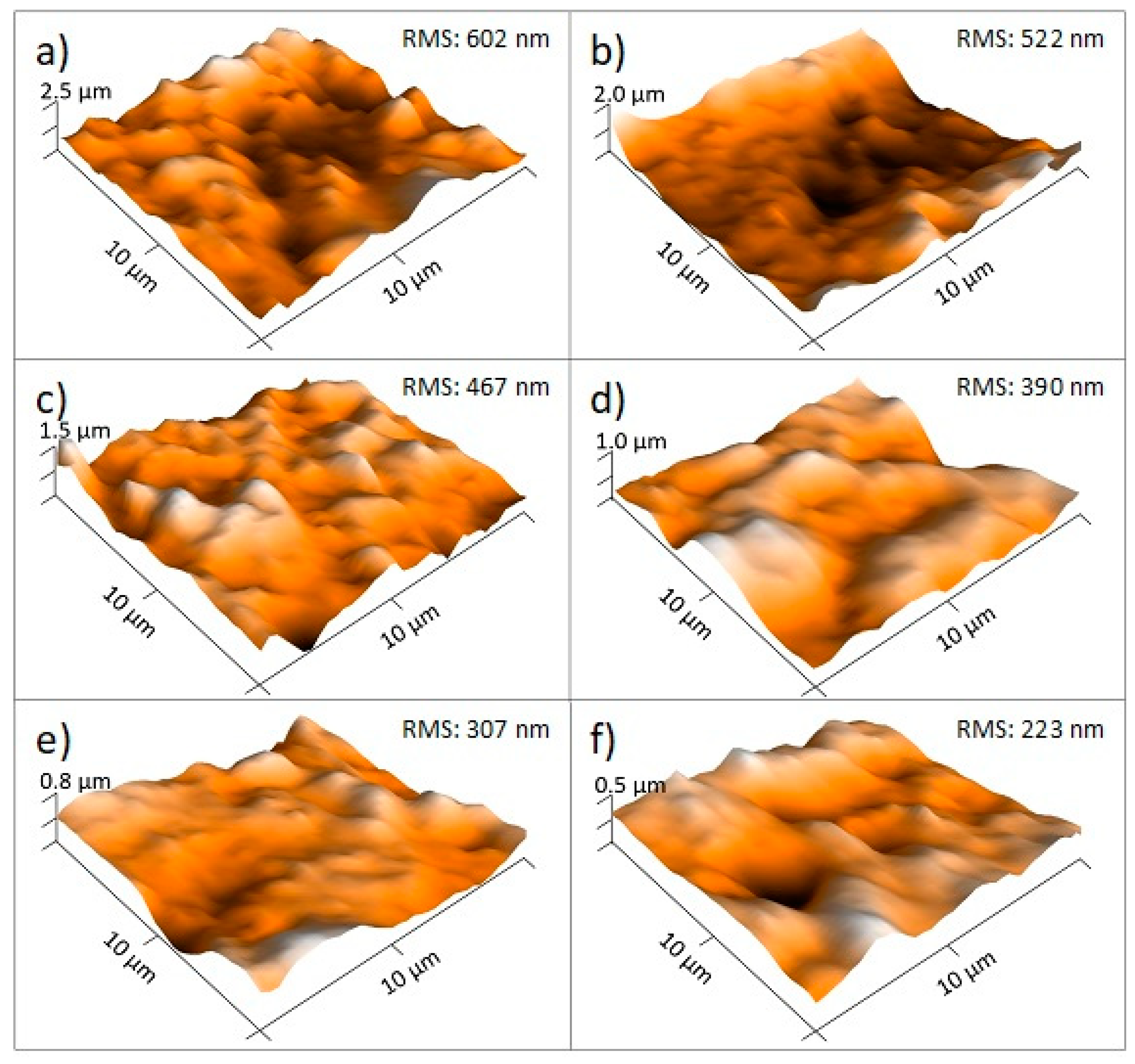
3.1. Atomic Force Microscopy (AFM)

The unpolished backside of the CdTe sample was subjected to AFM analysis to identify regions exhibiting comparable RMS roughness values. Figure 1 displays three-dimensional AFM images of six distinct areas on the crystal surface, each revealing a rough morphology. Corresponding RMS roughness values for these regions are as follows: (a) 602 nm, (b) 522 nm, (c) 467 nm, (d) 390 nm, (e) 307 nm, and (f) 223 nm. These areas were selected as representatives for subsequent PL and RRS measurements.
Following the AFM identification of regions with distinct RMS roughness values, PL and RRS measurements were conducted in these specific areas. The resulting spectral data are presented in the following sections.

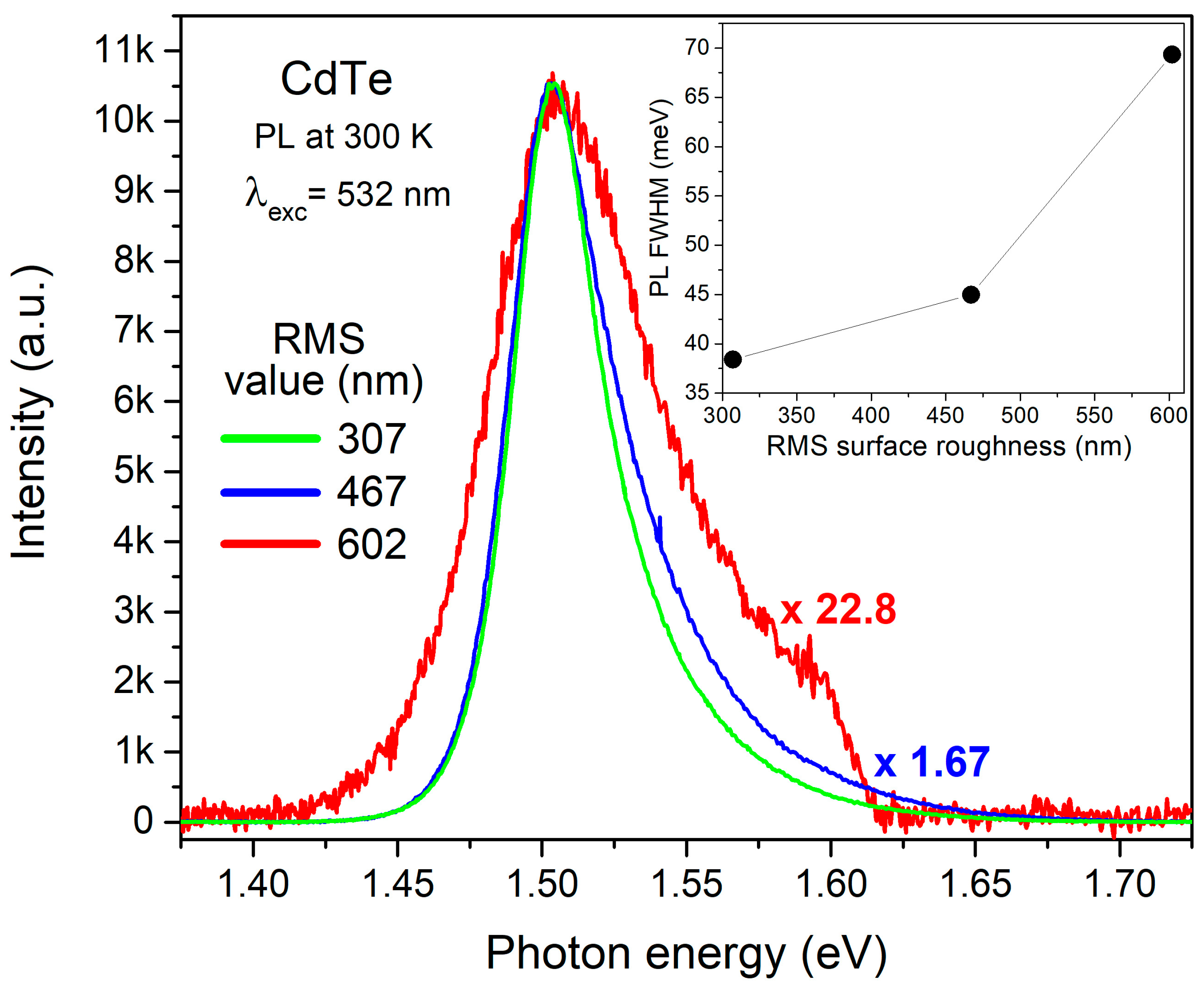
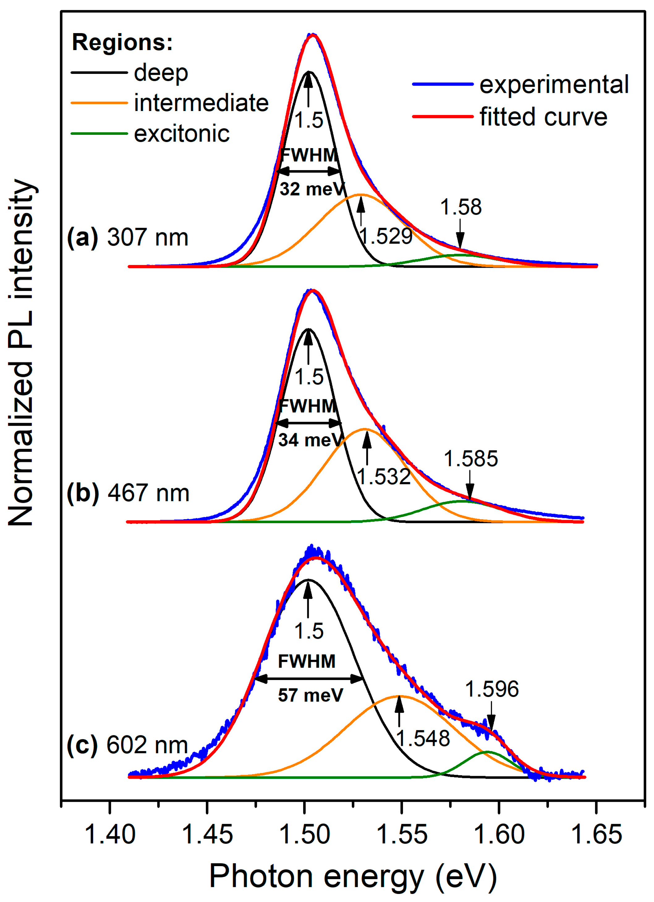
3.2. Photoluminescence (PL) Spectroscopy

Figure 2 shows the PL spectra obtained from three specific regions on the CdTe surface, characterized by RMS roughness values of 307 nm (green line), 467 nm (blue line), and 602 nm (red line). These regions were chosen for detailed analysis because of the significant differences in their respective PL emission spectra.
PL spectra exhibited a peak centered at 1.5 eV, consistent with the material’s bandgap energy. Notably, the peak position remained invariant across different surface roughness values. Conversely, PL intensity was significantly influenced by surface morphology. The spectrum acquired from the region with an RMS roughness of 307 nm displayed the highest signal intensity. To facilitate comparison, the spectra obtained for RMS values of 467 nm and 602 nm were normalized by factors of 1.67 and 22.8, respectively, relative to the 307 nm spectrum. Furthermore, a clear correlation was observed between spectral linewidth, quantified by the full width at half maximum (FWHM), and surface roughness.
As shown in Figure 2, increasing surface roughness led to a broader photoluminescence emission spectrum. The measured FWHM values for RMS roughness of 307 nm, 467 nm, and 602 nm were 38.42 meV, 44.98 meV, and 69.35 meV, respectively. This observed correlation between FWHM and surface roughness in CdTe is graphically illustrated in the inset of Figure 2. To the best of our knowledge, the correlation between the FWHM of the PL spectra and the RMS roughness of the CdTe surface is a novel finding.

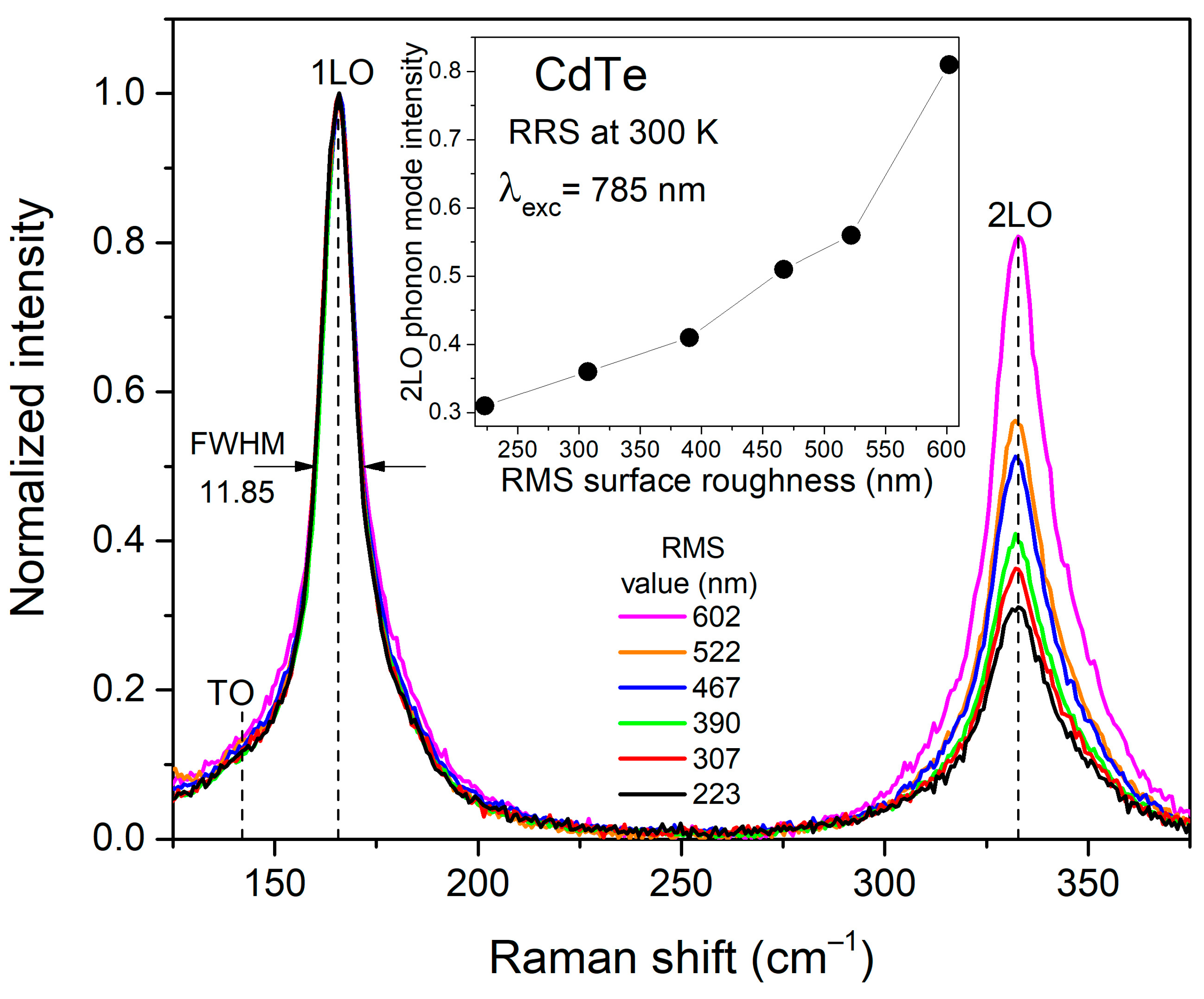
3.3. Resonant Raman Scattering (RRS) Spectroscopy

Figure 3 shows the evolution of the resonant Raman line shapes as a function of RMS surface roughness values, also indicated in the figure. The experimental spectra, represented by solid color lines, are plotted in the 125–375 cm−1 frequency range. For comparison, in all cases, the spectra have been normalized to 1LO phonon intensity to render features more evident.
The spectra in Figure 3 show two prominent main peaks, which have been labeled as 1LO and 2LO for the first-order longitudinal optical phonon at 165.7 cm−1 and its overtone located at 332.5 cm−1, respectively [27,28]. An overtone is a phonon whose frequency (ωn) is a multiple of the fundamental frequency (ω(LO)) so that it can be expressed as ωn = nω(LO), with n being the overtone number [29].
Figure 3 displays a vertical dashed line indicating an additional phonon mode in CdTe, attributed to the first-order transverse optical (TO) phonon at approximately 141 cm−1 [27]. Under resonant conditions, the TO Raman scattering cross-section is determined solely by the deformation potential. In contrast, the LO scattering cross-section arises from contributions of both the deformation potential and the Fröhlich interaction. Thus, the LO peak exhibits significantly higher intensity compared to the TO mode [27]. Moreover, unlike the sharp 1LO phonon peak with an FWHM of 11.85 cm−1, the 2LO phonon mode exhibits a broader profile. As shown in the inset of Figure 3, the intensity of the 2LO phonon mode is correlated with increasing surface roughness.

4. Discussion

In our PL measurements, the excitation source employs photons with energy greater than the bandgap of CdTe. These energetic photons are absorbed by the sample, promoting electrons from the valence band to the conduction band, thereby generating electron-hole pairs. Subsequently, these excited charge carriers relax to their ground state through various mechanisms. Radiative recombination processes, where electrons and holes recombine to emit photons, are the primary mechanisms responsible for the emission of light in PL spectroscopy.
Our results indicate that the PL peak position is unaffected by changes in surface roughness. The consistency of the PL peak position suggests that the energy level associated with the fundamental radiative transition in the material, such as the bandgap, remains unchanged regardless of surface roughness. Furthermore, the decrease in PL spectrum intensity can be attributed to increased light scattering caused by greater surface roughness. This leads to lower photoluminescence emission efficiency. Surface irregularities contribute to additional light scattering and absorption, reducing PL intensity.
On the other hand, the PL-emitted photon energy directly correlates with the energy difference between the involved electronic states, providing insights into the material’s bandgap and defect-related energy levels. For CdTe, these energy levels are primarily attributed to native point defects, extended defects, and impurities or even the interactions between them [30]. Such defects act as recombination and trapping centers, often referred to as surface states, which influence carrier dynamics and recombination pathways. The interplay between these factors results in broadened and asymmetric PL spectra.
Figure 4 shows the normalized PL spectra for regions with RMS roughness values of (a) 307 nm, (b) 467 nm, and (c) 602 nm. Blue lines represent experimental data. For clarity, spectra have been vertically offset. The experimental PL peaks shown in Figure 4 exhibit broad, asymmetric spectral profiles, suggesting the superposition of multiple emission processes. Here, deconvolution techniques can be employed to separate the composite peak into its individual components, providing insights into the physical mechanisms contributing to the overall emission.
To deconvolute the PL emission peak, we fitted each spectrum with three Gaussian functions corresponding to the deep, intermediate (also known as donor–acceptor pair or DAP), and excitonic spectral regions. We adopted this approach because the PL spectra of CdTe typically exhibit feature emissions in these three main spectral sections [31].
The deconvolution of the PL spectra into constituent Gaussian components reveals a primary peak centered on 1.5 eV, composed of three uniformly broadened Gaussian lines located at the position indicated by vertical arrows in Figure 4. The deconvolution results, represented by red lines, exhibit excellent agreement with the experimental data.
The dominant spectral component corresponds to the deep region, typically associated with defects. As our sample is undoped, intermediate and excitonic region intensities are negligible and their fitting parameters remain relatively constant with varying surface roughness. Consequently, these contributions were disregarded. Figure 4 demonstrates a correlation between the FWHM of the deep region and RMS surface roughness, suggesting that surface roughness promotes the formation of surface states, thereby influencing the material’s electronic structure.
The correlation between surface roughness and FWHM of the PL peak suggests that smoother areas have fewer surface states and reduced nonradiative recombination in the deep region. The recombination of charge carriers is a primary factor limiting the performance of CdTe devices, such as solar cells and detectors [32]. While detectors are often fabricated from single crystals, thin films are primarily used for commercial solar cells because of processing costs and the lack of large-diameter wafers of bulk CdTe [33]. Typically, a significant portion of charge carrier recombination in CdTe solar cells occurs at or near the surface, with surface recombination velocities often exceeding 105 cm/s [32,34]. However, work has shown that the dominant recombination losses occur in the bulk of the absorber. This is because of charged grain boundaries and interfacial carrier recombination, which limit open-circuit voltage (VOC) and efficiency [35,36]. Depositing buffer layers on the CdTe surface can modify these properties and potentially reduce recombination [36].
In this work, TRPL measurements were not conducted. A comprehensive literature search revealed no studies investigating the influence of surface roughness on the electrical properties of CdTe single crystal using TRPL. However, the literature does provide examples of TRPL being employed to characterize surface recombination velocity (SRV) in passivated CdTe surfaces [32]. It is well established that increased surface roughness correlates with a higher SRV [37]. Given that SRV is directly proportional to the density of surface states [18], a greater roughness implies a higher density of surface states. This correlation is consistent with the observed increase in PL FWHM from our results.
On the other hand, Figure 5 shows the 1LO and 2LO peaks of RRS spectroscopy. The open circles correspond to the average experimental data in Figure 3. The intensity of the 2LO phonon has been normalized to that of the 1LO peak. The principal peaks (blue lines) were fitted using Lorentzian functions centered at 165.7 and 332.5 cm−1 for the 1LO and 2LO phonon modes, respectively. In the base of 1LO phonon, a small peak located at 151 cm−1 was identified and is attributed to the surface optical (SO) phonon mode. An SO mode arises from the vibration of atoms in the near-surface region. Its frequency falls between the bulk TO and LO phonon frequencies of the material [27,28]. The SO mode is difficult to observe because of weak scattering; however, its intensity is amplified under RRS conditions. Thus, the TO mode around 141 cm−1 and the SO mode around 151 cm−1 were well identified with vertical dashed lines. Two Lorentzian functions centered on these positions were used to fit them. Notably, the TO mode is symmetry-forbidden in bulk CdTe(001) but becomes Raman-active because of surface-induced symmetry breaking [38].
Besides the TO and the SO phonon modes, a shoulder at the high-frequency side of the 1LO peak is observed. Similar Raman scattering was reported in polycrystalline CdTe thin film. This scattering has been attributed to the contribution of the 2LO–SO coupling mode [27]. The Raman fitting (red line) and observation of the SO mode in our CdTe single crystal indicate that the high-frequency shoulder of the 1LO peak is caused by multi-phonon processes. These processes involved the 2LO–SO coupling phonon modes.
Moreover, the broadening shape of the base of the 2LO peak can be perfectly fitted by the multi-phonon coupling of the SO mode with the 1LO phonon and its overtones. Thus, the peak value of the multi-phonon coupling between the SO and 1LO modes, denoted as 1LO+SO, is indicated by a vertical dashed line at 313 cm−1 in Figure 5. Similarly, a multi-phonon mode identified as 3LO−SO was observed at 348 cm−1 on the high-frequency side of the 2LO mode. The presence of both these modes in CdTe has been previously documented [27,28].
The red line in Figure 5 represents the final fitted curve. Notably, there is excellent agreement between the fit and the experimental data. Table 1 presents a comprehensive summary of the fitting parameters used to model the 1LO and 2LO peaks.
It is important to note that the fitting parameters associated with multi-phonon modes are unaffected by changes in RMS values, indicating their independence from surface roughness. Nevertheless, these peaks are essential for accurately reproducing the line shape around the 1LO and 2LO phonon regions.
Finally, to explain the correlation between surface roughness and the intensity of the 2LO phonon mode, it is important to consider its shorter wavelength compared to 1LO phonons. This inherent characteristic renders 2LO phonons more susceptible to crystal lattice imperfections induced by surface roughness. As a result, these phonons undergo heightened scattering because of surface irregularities. Moreover, under resonant excitation conditions, 2LO phonons can interact with other phonons throughout the Brillouin zone. These interactions between phonons often involve energy exchange, resulting in phonon–phonon coupling. When the energy exchanged during phonon–phonon coupling coincides with the energy of 2LO phonon mode, the intensity of this mode in the spectrum will be enhanced. The augmentation of surface roughness enhances the probability of the 2LO phonon mode participating in Raman scattering, thereby intensifying this resonance effect. Consequently, increasing surface roughness directly correlates with an elevated peak intensity of the 2LO phonon mode.

5. Conclusions

This study demonstrates a clear correlation between surface roughness and the electrical and vibrational properties of CdTe single crystals. Our findings reveal that, while the PL peak position remains unaffected by changes in surface roughness, increased roughness leads to a decrease in PL intensity, indicative of heightened light scattering. Additionally, a direct relationship was observed between increasing surface roughness and the FWHM of the PL peak. This effect is attributed to the formation of surface states induced by surface irregularities, which act as recombination and capture centers for charge carriers. Consequently, the introduction of additional energy levels associated with these defects significantly affects the electronic properties of undoped CdTe crystals.
Furthermore, our investigation reveals a notable variation in the 2LO phonon mode related to surface roughness. Specifically, the intensity of the 2LO phonon increases with greater surface roughness. This effect can be explained by the interaction of the 2LO phonon with other phonons across the entire Brillouin zone under resonant excitation conditions. These phonon–phonon interactions, which involve energy exchange, establish phonon–phonon coupling. When the exchanged energy matches the energy of the 2LO phonon mode, a resonance effect occurs, enhancing the participation of the 2LO mode in Raman scattering and resulting in a stronger spectral peak. Surface roughness facilitates these phonon interactions, particularly for the 2LO mode, creating a more favorable environment for resonance under resonant Raman excitation. Thus, the peak intensity increases with higher surface roughness.
The findings of this study are significant as they provide valuable insights into how surface roughness affects both the optical and vibrational properties of CdTe single crystals. Understanding these relationships is crucial for optimizing the performance of CdTe-based devices and materials.

Author Contributions

Conceptualization, C.I.M.-R. and R.C.; Formal Analysis, C.I.M.-R., R.C., J.R.S.-E. and F.J.C.-R.; Investigation, C.I.M.-R., R.C., J.R.S.-E. and F.J.C.-R.; Methodology, C.I.M.-R.; Writing—Original Draft Preparation, C.I.M.-R. and R.C.; Writing—Review and Editing, C.I.M.-R., R.C., J.R.S.-E. and F.J.C.-R. All authors have read and agreed to the published version of the manuscript.

Funding

The authors would also like to acknowledge the financial support from project 276959 of the 2024 announcement of “Programa de Apoyo a la Mejora de las Condiciones de Producción de los Miembros del SNI y SNCA (PROSNI 2024)” of the Universidad de Guadalajara.

Institutional Review Board Statement

Not applicable.

Informed Consent Statement

Not applicable.

Data Availability Statement

The original contributions presented in the study are included in the article, further inquiries can be directed to the corresponding author.

Acknowledgments

Carlos I. Medel-Ruiz thanks Ángel Gabriel Rodríguez Vázquez, from the UASLP—México, for the technical support provided for the PL measurements.

Conflicts of Interest

The authors declare no conflicts of interest.

References

  1. Biswas, K.; Du, M.H. What causes high resistivity in CdTe. New J. Phys. 2012, 14, 063020. [Google Scholar] [CrossRef]
  2. Ghislotti, G.; Ielmini, G.; Riedo, E.; Martinelli, M.; Dellagiovanna, M. Picosecond time-resolved luminescence studies of recombination processes in CdTe. Solid State Commun. 1999, 111, 211–216. [Google Scholar] [CrossRef]
  3. Scarpulla, M.A.; McCandless, B.; Phillips, A.B.; Yan, Y.; Heben, M.J.; Wolden, C.; Xiong, G.; Metzger, W.K.; Mao, D.; Krasikov, D.; et al. CdTe-based thin film photovoltaics: Recent advances, current challenges and future prospects. Sol. Energy Mater. Sol. Cells 2023, 255, 112289. [Google Scholar] [CrossRef]
  4. Gnatyuk, V.; Maslyanchuk, O.; Solovan, M.; Brus, V.; Aoki, T. CdTe X/γ-ray detectors with different contact materials. Sensors 2021, 21, 3518. [Google Scholar] [CrossRef] [PubMed]
  5. Ahmad, N.I.; Kar, Y.B.; Doroody, C.; Kiong, T.S.; Rahman, K.S.; Harif, M.N.; Amin, N. A comprehensive review of flexible cadmium telluride solar cells with back surface field layer. Heliyon 2023, 9, e21622. [Google Scholar] [CrossRef] [PubMed]
  6. Hakeem, A.A.; Ali, H.M.; Abb El-Raheem, M.M.; Hasaneen, M.F. Study the effect of type of substrates on the microstructure and optical properties of CdTe thin films. Optik 2021, 225, 165390. [Google Scholar] [CrossRef]
  7. Campos-González, E.; de Moure-Flores, F.; Ramírez-Velázquez, L.E.; Casallas-Moreno, K.; Guillén-Cervantes, A.; Santoyo-Salazar, J.; Contreras-Puente, G.; Zelaya-Angel, O. Structural and optical properties of CdTe-nanocrystals thin films grown by chemical synthesis. Mater. Sci. Semicond. Process. 2015, 35, 144–148. [Google Scholar] [CrossRef]
  8. Gunjal, S.D.; Khollam, Y.B.; Jadkar, S.R.; Shripathi, T.; Sathe, V.G.; Shelke, P.N.; Takwale, M.G.; Mohite, K.C. Spray pyrolysis deposition of p-CdTe films: Structural, optical and electrical properties. Sol. Energy 2014, 106, 56–62. [Google Scholar] [CrossRef]
  9. Ablekim, T.; Duenow, J.N.; Zheng, X.; Moutinho, H.; Moseley, J.; Perkins, C.L.; Johnston, S.W.; O’Keefe, P.; Colegrove, E.; Albin, D.S.; et al. Thin-Film Solar Cells with 19% Efficiency by Thermal Evaporation of CdSe and CdTe. ACS Energy Lett. 2020, 5, 892–896. [Google Scholar] [CrossRef]
  10. Mathew, X.; Mathews, N.R.; Sebastian, P.J.; Flores, C.O. Deep levels in the band gap of CdTe films electrodeposited from an acidic bath—PICTS analysis. Sol. Energy Mater. Sol. Cells. 2004, 81, 397–405. [Google Scholar] [CrossRef]
  11. Lugo, J.M.; Rosendo, E.; Romano-Trujillo, R.; Oliva, A.I.; de Guevara, H.P.L.; Medel-Ruiz, C.I.; Treviño-Yarce, L.; Sarmiento Arellano, J.; Morales, C.; Díaz, T.; et al. Effects of the applied power on the properties of RF-sputtered CdTe films. Mater. Res. Express. 2019, 6, 076428. [Google Scholar] [CrossRef]
  12. Tang, K.; Zhu, X.; Bai, W.; Zhu, L.; Bai, J.; Dong, W.; Yang, J.; Zhang, Y.; Tang, X.; Chu, J. Molecular beam epitaxial growth and optical properties of the CdTe thin films on highly mismatched SrTiO3 substrates. J. Alloys Compd. 2016, 685, 370–375. [Google Scholar] [CrossRef]
  13. Krč, J.; Zeman, M.; Kluth, O.; Smole, F.; Topič, M. Effect of surface roughness of ZnO: Al films on light scattering in hydrogenated amorphous silicon solar cells. Thin Solid Films 2003, 426, 296–304. [Google Scholar] [CrossRef]
  14. Vyas, P.B.; Van de Put, M.L.; Fischetti, M.V. Master-equation study of quantum transport in realistic semiconductor devices including electron-phonon and surface-roughness scattering. Phys. Rev. Appl. 2020, 13, 014067. [Google Scholar] [CrossRef]
  15. Mori, K.; Samata, S.; Mitsugi, N.; Teramoto, A.; Kuroda, R.; Suwa, T.; Hashimoto, K.; Sugawa, S. Influence of silicon wafer surface roughness on semiconductor device characteristics. Jpn. J. Appl. Phys. 2020, 59, SMMB06. [Google Scholar] [CrossRef]
  16. Xie, S.; Zhu, H.; Zhang, X.; Wang, H. A brief review on the recent development of phonon engineering and manipulation at nanoscales. Int. J. Extreme Manuf. 2023, 6, 012007. [Google Scholar] [CrossRef]
  17. Chen, J.; Xu, K. Applications of atomic force microscopy in materials, semiconductors, polymers, and medicine: A minireview. Instrum. Sci. Technol. 2020, 48, 667–681. [Google Scholar] [CrossRef]
  18. Gfroerer, T.H. Photoluminescence in analysis of surfaces and interfaces. Encycl. Anal. Chem. 2000, 67, 3810. [Google Scholar] [CrossRef]
  19. Cannas, M.; Vaccaro, L. Time-Resolved Photoluminescence. In Spectroscopy for Materials Characterization, 1st ed.; Agnello, S., Ed.; John Wiley & Sons: Hoboken, NJ, USA, 2021; Volume 3, pp. 35–58. [Google Scholar]
  20. Kuciauskas, D.; Kanevce, A.; Dippo, P.; Seyedmohammadi, S.; Malik, R. Minority-carrier lifetime and surface recombination velocity in single-crystal CdTe. IEEE J. Photovolt. 2015, 5, 366–371. [Google Scholar] [CrossRef]
  21. Jones, R.R.; Hooper, D.C.; Zhang, L.; Wolverson, D.; Valev, V.K. Raman Techniques: Fundamentals and Frontiers. Discov. Nano 2019, 14, 231. [Google Scholar] [CrossRef]
  22. Schmitt, M.; Popp, J. Raman spectroscopy at the beginning of the twenty-first century. J. Raman Spectrosc. 2006, 37, 20–28. [Google Scholar] [CrossRef]
  23. Kusch, P.; Grelich, E.; Somaschini, C.; Luna, E.; Ramsteiner, M.; Geelhaar, L.; Riechert, H.; Reich, S. Type-II band alignment of zinc-blende and wurtzite segments in GaAs nanowires: A combined photoluminescence and resonant Raman scattering study. Phys. Rev. B 2014, 89, 045310. [Google Scholar] [CrossRef]
  24. Sathya, B.; Benny Anburaj, D.; Porkalai, V.; Nedunchezhian, G. Raman scattering and photoluminescence properties of Ag doped ZnO nano particles synthesized by sol–gel method. J. Mater. Sci. Mater. Electron. 2017, 28, 6022–6032. [Google Scholar] [CrossRef]
  25. Fonthal, G.; Tirado-Mejía, L.; Marín-Hurtado, J.I.; Ariza-Calderón, H.; Mendoza-Álvarez, J.G. Temperature dependence of the band gap energy of crystalline CdTe. J. Phys. Chem. Solids. 2000, 61, 579–583. [Google Scholar] [CrossRef]
  26. Akin, N.; Ozen, Y.; Efkere, H.I.; Cakmak, M.; Ozcelik, S. Surface structure and photoluminescence properties of AZO thin films on polymer substrates. Surf. Interface Anal. 2015, 47, 93–98. [Google Scholar] [CrossRef]
  27. Li, X.; Liu, D.; Wang, D. Anharmonic phonon decay in polycrystalline CdTe thin film. Appl. Phys. Lett. 2018, 112, 252105. [Google Scholar] [CrossRef]
  28. Liu, D.; Chen, J.; Wang, D.; Wu, L.; Wang, D. Enhanced surface optical phonon in CdTe thin film observed by Raman scattering. Appl. Phys. Lett. 2018, 113, 061604. [Google Scholar] [CrossRef]
  29. Prasad, N.; Karthikeyan, B. Resonant and Off-Resonant Phonon Properties of Wurtzite ZnS: Effect of Morphology on Fröhlich Coupling and Phonon Lifetime. J. Phys. Chem. C. 2018, 122, 18117–18123. [Google Scholar] [CrossRef]
  30. Musiienko, A.; Grill, R.; Hlídek, P.; Moravec, P.; Belas, E.; Zázvorka, J.; Korcsmáros, G.; Franc, J.; Vasylchenko, I. Deep levels in high resistive CdTe and CdZnTe explored by photo-Hall effect and photoluminescence spectroscopy. Semicond. Sci. Technol. 2016, 32, 015002. [Google Scholar] [CrossRef]
  31. Feng, Z.C.; Li, Q.; Wan, L.; Xu, G. Variation of phonon coupling factors in the photoluminescence of cadmium telluride by variable excitation power. Opt. Mater. Express 2017, 7, 808–816. [Google Scholar] [CrossRef]
  32. Reese, M.O.; Perkins, C.L.; Burst, J.M.; Farrell, S.; Barnes, T.M.; Johnston, S.W.; Kuclauskas, D.; Gesser, T.A.; Metzger, W.K. Intrinsic surface passivation of CdTe. J. Appl. Phys. 2015, 118, 155305. [Google Scholar] [CrossRef]
  33. Jovanovic, S.M.; Devenyi, G.A.; Jarvis, V.M.; Meinander, K.; Haapamaki, C.M.; Kuyanov, P.; Gerber, M.; LaPierre, R.R.; Preston, J.S. Optical characterization of epitaxial single crystal CdTe thin films on Al2O3 (0001) substrates. Thin Solid Films 2014, 570, 155–158. [Google Scholar] [CrossRef]
  34. Kuciauskas, D.; Krasikov, D. Spectroscopic and microscopic defect and carrier-lifetime analysis in cadmium telluride. IEEE J. Photovolt. 2018, 8, 1754–1760. [Google Scholar] [CrossRef]
  35. Kuciauskas, D.; Moseley, J.; Lee, C. Identification of Recombination Losses in CdSe/CdTe Solar Cells from Spectroscopic and Microscopic Time-Resolved Photoluminescence. Sol. RRL 2021, 5, 2000775. [Google Scholar] [CrossRef]
  36. Paul, S.; Swartz, C.; Sohal, S.; Grice, C.; Bista, S.S.; Li, D.B.; Yan, Y.; Holtz, M.; Li, J.V. Buffer/absorber interface recombination reduction and improvement of back-contact barrier height in CdTe solar cells. Thin Solid Films 2019, 685, 385–392. [Google Scholar] [CrossRef]
  37. Flores-Mendoza, M.A.; Castanedo-Pérez, R.; Torres-Delgado, G.; Cruz-Orea, A.; Mendoza-Alvarez, J.G.; Zelaya-Angel, O. Surface Recombination Velocity Dependence on Morphological Properties of CdTe Thin Films Prepared by Close-Spaced Sublimation. Int. J. Thermophys. 2013, 34, 1746–1753. [Google Scholar] [CrossRef]
  38. Amirtharaj, P.M.; Pollak, F.H. Raman scattering study of the properties and removal of excess Te on CdTe surfaces. Appl. Phys. Lett. 1984, 45, 789–791. [Google Scholar] [CrossRef]
Figure 1. Atomic force microscopy (AFM) images of cadmium telluride (CdTe) regions with various root-mean-square (RMS) values: (a) 602 nm, (b) 522 nm, (c) 467 nm, (d) 390 nm, (e) 307 nm, and (f) 223 nm.
Applsci 14 07680 g001
Figure 2. Photoluminescence (PL) spectra of CdTe with different root-mean-square (RMS) values. The inset shows the correlation between the full width at half maximum (FWHM) and the RMS value of roughness.
Applsci 14 07680 g002
Figure 3. Experimental resonant Raman scattering (RRS) spectra of CdTe for different RMS surface roughness values. The inset shows the correlation between the intensity of the 2LO phonon mode and the RMS value of roughness.
Applsci 14 07680 g003
Figure 4. PL spectra of CdTe for three surfaces with RMS roughness values of (a) 307 nm, (b) 467 nm, and (c) 602 nm. The colored lines correspond to the experimental data (blue), fitted curve (red), and individual Gaussian contributions (other colors).
Applsci 14 07680 g004
Figure 5. Experimental 1LO and 2LO data (open circles) and spectra fittings (red line) correspond to decomposition on elementary contributions (colored lines).
Applsci 14 07680 g005
Table 1. Values of the parameters used to fit the RRS line shape shown in Figure 5.
Phonon ModePeak Position
(cm−1)
FWHM
(cm−1)
Intensity
TO141140.05
SO151160.035
1LO165.711.80.955
2LO−SO180.5200.095
1LO+SO313200.05
2LO332.5180.95
3LO−SO348200.12
Disclaimer/Publisher’s Note: The statements, opinions and data contained in all publications are solely those of the individual author(s) and contributor(s) and not of MDPI and/or the editor(s). MDPI and/or the editor(s) disclaim responsibility for any injury to people or property resulting from any ideas, methods, instructions or products referred to in the content.

