Article

Cascaded Frequency Selective Surfaces with Matryoshka Geometry for Ultra-Wideband Bandwidth

1
Department of Electrical Engineering, Federal University of Campina Grande (UFCG), Campina Grande 58429-900, PB, Brazil
2
Polytechnic School of Pernambuco, University of Pernambuco (UPE), Recife 50720-001, PE, Brazil
*
Author to whom correspondence should be addressed.
Appl. Sci. 2024, 14(19), 8603; https://doi.org/10.3390/app14198603
Submission received: 8 August 2024 / Revised: 16 September 2024 / Accepted: 17 September 2024 / Published: 24 September 2024

Abstract

:
The purpose of this paper is to present cascaded frequency selective surfaces (FSSs) with matryoshka geometry to increase the effective bandwidth. We carry out an analysis of the influence of the spacing between the surfaces on the FSSs frequency response. The application involves a two-layer cascaded FSS, one as a band-stop filter with a matryoshka geometry and the other as a band-pass filter with inverted or negative matryoshka geometry. With this framework, it is possible to extend an ultra-wideband (UWB) of a bandwidth up to 2 GHz in the 1.8 GHz to 3.8 GHz range with just two layers and an air gap of 12 mm, in addition to a bandwidth of 2 GHz to 3.2 GHz with a smaller 4 mm gap between layers.

1. Introduction

Research and development on frequency selective surfaces (FSSs) using microstrips in a wide variety of applications has been addressed in many works [1,2,3,4,5]. The most well-known example of FSS application is the common microwave shield, but there are also uses such as radomes [6,7] to protect the antenna system (typically radar antennas) from atmospheric agents such as wind, rain, snow, hail, and hot temperatures while also optimizing the signal reception. Another example of FSS application is in sub-reflectors [8], which optimize the signal received by an antenna.
More recent uses of FSSs include smart windows [9,10], which favor the signals by attenuating the noise and redirecting only the spectral components that are within desired frequency ranges, and wearable microstrips [11], which are circuits printed on fabrics like jeans to be used in clothes. For 5G applications, FSSs are used to improve the signals of reception and transmission, either by blocking unwanted signals or reflecting them to improve antenna performance. Other potential uses of FSSs include dual-band operation, the provision of electromagnetic shielding, and potential near-field applications [12].

1.1. Review

FSSs are two-dimensional periodic arrays of electric-metallic elements that present behavior similar to that of electromagnetic filters. One of their possible configurations is presented in Figure 1 for an example of matryoshka geometry. These structures are designed for the purpose of reflecting or transmitting electromagnetic waves in different frequency bands. Such characteristics can be observed according to the type of element used in the arrangement, whether it is a patch or opening type, which directly influences the frequency response of the FSS, which may have band-reject or band-pass characteristics, respectively.
In addition to the type of element, the geometry, the periodicity of the arrangement, the number and thickness of layers, the angle of incidence of the plane wave, and the dielectric on which the FSS is printed are factors that affect the performance and frequency response of an FSS [13,14].
Although the simple single-layer FSS is easy to fabricate, it is difficult to improve the bandwidth. This kind of FSS has a limitation that, in recent years, with the development of antennas with larger bandwidth, is becoming more and more cumbersome [15]. One of the solutions for this limitation is the design of FSSs with multiple layers, creating an optimized filter and a multiband performance on the frequency response, as will be seen in the examples ahead.
Research on microstrips includes the development of new and different geometries, as well as the addition of methods to produce different results that may optimize the application of antenna electromagnetic waves. According to some studies [1,2,5,14,15], FSS structures can be represented by an equivalent circuit, considering the transverse electric mode, TE, and transverse magnetic mode, TM, incidence on conductive strips.
The equivalent circuits have a formula for the number of inductors and capacitors as well as their positions in series or parallel for each geometry and can be seen as a model of what kind of filter they represent in the frequency response. For example, a square ring geometry’s equivalent circuit is one inductor and one capacitor in series.
The design of geometries, from the basic solid squares and circle rings to the fractals, has been a topic of research in FSS in many papers over the last few years [16,17,18,19,20,21,22,23,24,25,26].
The design in [16] presents four different stages of two distinct fractal geometries: one is the traditional Sierpinski fractal, and the other is an improved version. There is also an analysis of the FSS frequency response implemented with each stage for both fractals, showing their resonance frequency and bandwidth. Additionally, Chen et al. [16] present an analysis of the measured frequency response of the FSS with the improved fractal geometry for different angles of incidence to demonstrate the effect of the transverse electric (TE) polarization and transverse metallic (TM) polarization. The paper [16] also presents a comparison of both geometries in the fourth stage. The improved design of the Sierpinski fractal is a good example of a geometry with stability to the incidence angle of polarization and bandwidths of 910 MHz and 1630 MHz at resonant frequencies 2.4 GHz and 5.45 GHz. In the present paper, a cascaded FSS with matryoshka geometry presents the advantage of reaching a larger bandwidth, around 2.4 GHz. This bandwidth includes frequencies from 1.8 GHz to 3.8 GHz, with applications for the 2.0 GHz band, the 5G in 3.5 GHz, and the wireless local-area network (WLAN) frequency range, as proposed for shielding in [16].
A single square ring geometry on multiple layers is proposed in [17], using a total of four layers in their cascaded FSS to provide an absorption on a bandwidth of more than 3 GHz, from 2.4 GHz to 6.13 GHz.
The FSSs are designed with a simple square ring geometry and the same FR-4 in each layer. The metallic surface of the FSSs is modified into a resistive material for two layers and into a conductive material for the other two. The resistive layer is a dielectric material covered with a thin film of nickel-phosphorus, while the conductive surface is a simple copper material. Simulations were carried out, and measures were obtained of the cascaded FSS for two different spacings between the layers, 5 mm and 10 mm, with comparisons between the spacings and between simulated and measured results. The design in [17] is an absorber cascaded FSS of four layers for a frequency range from 2.48 GHz to 6.13 GHz and a bandwidth higher than 3 GHz. The main advantage of the structure presented by Peixoto Neto [17] is the absorption of signals for the entire industrial, scientific, and medical (ISM) radio band from 2.4 GHz to 2.4835 GHz, 5G at 3.5 GHz, and unlicensed national information infrastructure (UNII) from 5 GHz to 6 GHz. The cascaded FSS with matryoshka geometry proposed in the present paper presents a range that covers 2.0 GHz, the ISM band, and 5G at 3.5 GHz with only two layers and is easier to fabricate with only metallic layers. These advantages are especially useful for applications requiring a large bandwidth at lower frequencies.
The development of a cascaded FSS is presented in [18] with a geometry of two concentric square rings to provide a large bandwidth with only two layers of FSS, a characteristic portrayed here in this paper. However, in [18], a 5 cm gap between the layers is proposed, and the bandwidth for the measured result is from 3 GHz to 11.64 GHz, a wide range of more than 8 GHz that influences frequencies beyond 10 GHz. However, this wide range comes with a larger spacing between the layers. The cascaded FSS with matryoshka geometry in the present work does not have such a wide range, but it uses only 12 mm spacing, more than four times less space, and includes the earlier frequencies of 1.8 GHz.
In a paper by Silva Segundo et al. [19], a design is presented of a three-layer cascaded FSS with patch and slotted patch geometry and 10 mm spacing between the layers. This structure allows obtaining a band-stop for ultra-wideband (UWB) applications with a bandwidth of 7.5 GHz between 3.10 GHz and 10.6 GHz. The paper shows the analysis of the resonant frequencies of the individual FSS layers and their influence on the cascaded FSS, as well as comparisons between the simulated designed model and the measurement of the fabricated FSSs. When comparing the design in [19] with the cascaded FSS with matryoshka geometry in the present paper, the design of [17] shows a larger bandwidth, but only for frequencies above 3 GHz, and a total gap of 20 mm between all three layers.
There are also examples that explore dual-band operation [20,21], in which the resonance frequencies occur in two different bands, and innovative uses, such as a three-dimensional origami-like FSS [20] or a curved metal FSS [21]. The FSS presented in [20] reaches smaller bandwidths of less than 600 MHz, and the FSS design in [21] has a resonance frequency of 10 GHz. The designed cascaded FSS with matryoshka geometry in our paper presents an optimized way to reach an ultra-wideband from 1.8 GHz to 3.8 GHz frequency range with only two layers spaced by 12 mm.
Another innovative FSS structure is presented in [22], in which a metasurface filter of vanadium dioxide (VO2) with a switchable mode of transmission/reflection for electromagnetic shielding applications is designed. The paper by Wang et al. [22] shows a design with hybrid layers and its components, as well as numerical analysis by finite element method (FEM). There is also a study of the equivalent circuit model (ECM) in which the FSS geometry can be analyzed as a circuit composed of inductors and capacitors. Although this is an innovative design, its bandwidth and applications are for terahertz frequencies, ranging from 0.1 THz to 3.78 THz. When compared with the cascaded FSS of matryoshka geometry design in the present work, they are not as suitable for the 1 to 5 GHz range, where many applications are in use.
There are also other FSSs that have several modern applications. An example is found in the work of Yunos et al. [23], which addresses how FSSs can contribute to buildings with architecture covered by many panes of glass, reducing the consumption of electricity involved in cooling and heating while leading to adequate transmission of electromagnetic waves carrying telecommunications signals through the windows. Low-emissivity (low-e) windows have been proposed as a solution to minimize energy use as they are capable of reflecting external heat radiation, thus reducing cooling loads when compared to conventional windows. Low-e windows have been used in both architectural and automotive sectors to block ultraviolet (UV) and infrared (IR) radiation from the sun. The windows are made with thin multilayer coatings (metallic and dielectric layers), which are highly transparent to visible light but reflect infrared radiation (heat). However, metallic layers attenuate telecommunications signals, such as radio frequency (RF) and microwave signals. Due to the demand for reliable mobile communications coverage, those windows need to be transparent to waves in the frequency ranges of these signals. One technology that can solve this problem is frequency selective surface (FSS), which can be incorporated into the surface of windows to selectively filter electromagnetic waves.
Another application of FSSs is presented in [24], in which the authors propose a flexible and reconfigurable monopole antenna design with FSS for Internet of Things (IoT) applications. To improve the antenna gain, a simple FSS was designed to be placed under the antenna at a distance of 15 mm. FSS operates efficiently in the 2 to 4.5 GHz band and has improved antenna gain. Maximum gains of 6.5 dBi, 7.52 dBi, and 7.91 dBi were achieved in the three frequency bands under consideration.
In [25], an FSS is associated with a microstrip antenna to obtain ultra-wideband (UWB). The antenna contains a hexagonal patch with multiple inserted stubs to provide an ultra-wideband range from 5 GHz to 17 GHz. Results show that the aforementioned approach is a strong candidate for future high-gain, high-bandwidth wireless devices.
A radiating element consisting of a modified circular patch is proposed in [26] for MIMO arrays in 5G millimeter-wave applications. The radiating elements of the proposed 2 × 2 antenna array are configured orthogonally to each other to mitigate mutual coupling that would otherwise degrade the performance of the MIMO system. Due to the low coupling between the radiating elements, its envelope correlation coefficient (ECC) is less than 0.002, and its diversity gain (DG) is greater than 9.99 dB in the 5G operating band centered at 28 GHz between 26.5 GHz and 29.5 GHz.
An aperture antenna array shared between the Ku and Ka frequency bands, with high performance provided by an FSS, is evaluated in [27] in terms of gain, efficiency, and isolation between frequency bands. The antenna consists of two dipole arrays, one 8 × 8 for the Ka-band and the other 4 × 4 for the Ku-band. The proposed structure is composed of the 8 × 8 array printed on the top face of the substrate, a low-pass FSS printed on the opposite face of the substrate, and the 4 × 4 array printed on the top face of a second substrate so that the two arrangements form a sandwich with the FSS. The proposed antenna array presents an impedance bandwidth of −10 dB equal to 19.07% from 14.47 GHz to 17.52 GHz and 23.66% from 30.19 GHz to 38.29 GHz, with peaks gain of 18.9 dBi at 16 GHz and 24.85 dBi at 35 GHz, respectively.
A band-pass FSS with low insertion loss and angular stability, in relation to the variation of the horizontal angle of incidence of the wavefront, composed of three metallic layers, is proposed in [28]. The upper and lower metal layers are coupled through a metal ring layer to form the FSS structure. The equivalent circuit model is derived to explain the operating principle of the proposed FSS. In the design, two transmission zeros (TZs) are generated on both sides of the passband, contributing to the high selectivity performance of the structure. Furthermore, the surface distributions of electric current are provided for the analysis of the TZs generation mechanism. The performance of the proposed FSS is insensitive to the polarization and horizontal angle of incidence of the incident wave. To assess performance, a prototype of the FSS was manufactured, and the obtained results corroborated the simulations.
In [29], a metallic circular polarizer based on a band-pass FSS is presented that converts the linear polarization of the incident wave to a circular polarization in the Ka-band. In the case where the wavefront is incident parallel to the surface of the FSS, the polarizer operates in the frequency range of 27.5 GHz to 30.1 GHz, and in the case where the wavefront is incident oblique to the surface of the FSS, the operating frequency range is reduced.
An FSS-based electromagnetic energy absorber, insensitive to incident wave polarization and with ultra-wide bandwidth, is proposed in [30] for applications in the S- to K-bands. The absorber is formed by two compensation plates, a lossy FSS layer, and a grounded dielectric plate. The FSS unit cell geometry is a combination of a second-order Chinese knot and a cross.
Another promising application of FSS is to aid electronic material detection and identification systems. This task is crucial in many situations, such as waste classification and hazardous materials detection. Although existing systems based on radio frequency (RF) signals have achieved great success, they have limited identification accuracy when RF signals cannot penetrate through the target or when a target has different external and internal materials. In [31], a high-precision material identification system is proposed based on an FSS tag, also called FSS-Tag, which uses both incident signals and the effect of electromagnetic coupling. Specifically, an FSS tag was designed and attached to a target material, and the frequency response of the tag was then used for material detection since different target materials have different frequency responses.
FSS is also considered in [32] as a basis for the proposal of a dual-polarization angle-selective surface (ASS) based on a dual-layer FSS to achieve angular selectivity. By properly constructing the single-layer FSS structure, band-pass and band-reject modes of operation are produced by the ASS under normal and oblique incidences, respectively, resulting in angular selectivity. The proposed ASS can play an important role in many applications, such as minimizing the sidelobes of an antenna.
A type of electromagnetic shield based on an FSS operating in dual-band and insensitive to the polarization of the incident wave is proposed in [33]. The FSS miniaturized unit cell consists of a modified Jerusalem cross loop and a modified square loop at the cell corners. The proposed configuration is a potential candidate for RF shielding/isolation applications.
Regarding manufacturing procedures, in [34], the authors present the design and manufacture of an FSS for the THz band based on the joint application of two distinct technologies, called printable electronics (PE) and three-dimensional (3D) printing. The rotational tuning approach was applied to two identical FSSs to form a reconfigurable FSS called Moiré FSS. Based on the numerical results obtained, it was possible to verify that the proposed technique that used the PE-based Moiré FSS achieved a modulation depth of 58% at 0.25 THz, while the experimental verification presented a modulation depth of 41% at 0.22 THz, confirming that its adoption is economically viable and effective.
In [35], a tri-band-pass FSS is presented that achieves high-order filtering responses in different frequency ranges through a complementary FSS structure, also called negative FSS. The simulation results indicate that the developed FSS can present three passbands around 3.79 GHz, 8.34 GHz, and 12.52 GHz. The fractional bandwidths at 3 dB are 52.8%, 13.7%, and 19.7%, respectively. The frequency responses, in terms of transmission coefficient, show rapid transfer from the passband to the rejection band and there is significant out-of-band suppression between adjacent passbands.
In [36], a new procedure is proposed for designing topologies with many degrees of freedom (DoFs). The authors propose an inverse topological design method (ITDM) based on machine learning for FSS structures. An efficient training dataset construction strategy is proposed based on several classical FSS structures.
Machine learning is also considered in [37] in the efficient design of FSS structures with many degrees of freedom (DoFs). A spatial inverse design method (SIDM) is proposed based on machine learning technology. This SIDM takes advantage of inverse modeling and topological design to spatially design the FSS. Unlike simple parametric or topological modeling, which involves only one type of variable, i.e., binary or continuous, the proposed SIDM contains binary and continuous variables to model FSS flexibly and at a lower cost. A multilayer perceptron (MLP) neural network is employed to capture the characteristics of both types of variables and perform the mapping of the EM response onto the corresponding FSS structure.

1.2. Contributions

The original matryoshka geometry is portrayed in [38] and has been studied by different researchers. Among variations of the original design, the polarization-independent circular matryoshka [39] was developed, which then inspired the square version used in [40] and in this work. The most recent application was the square matryoshka geometry in a defective ground structure (DGS) [41]. In this paper, we propose the use of the square matryoshka geometry and its negative geometry in a cascaded FSS structure.
This paper presents the development and analysis of the cascaded FSS with square matryoshka geometry to provide a bandwidth that, depending on the variation in the gap between the FSSs, can be greater than 1 GHz in the range from 1.8 GHz to 3.8 GHz. When compared with other papers on the subject, their projected structures do not have frequency ranges below 2.4 GHz and bandwidth of 2 GHz with a two-layer 12 mm spaced FSS. Other designs that present larger bandwidths require more layers and greater spacing between them or have bandwidths above 3.0 GHz. Thus, the design in the present paper has the advantages of using less spacing between layers, fewer layers, being easier to manufacture, and reaching lower frequencies, as shown in Table 1 and Table 2.
In this paper, we present the following contributions:
  • Project, simulation, and validation of a cascaded FSS using matryoshka geometry, which is more efficient in cell dimensions in comparison with concentric square rings.
  • Frequency response evaluation of the proposed structure in the band around 1.8 GHz.
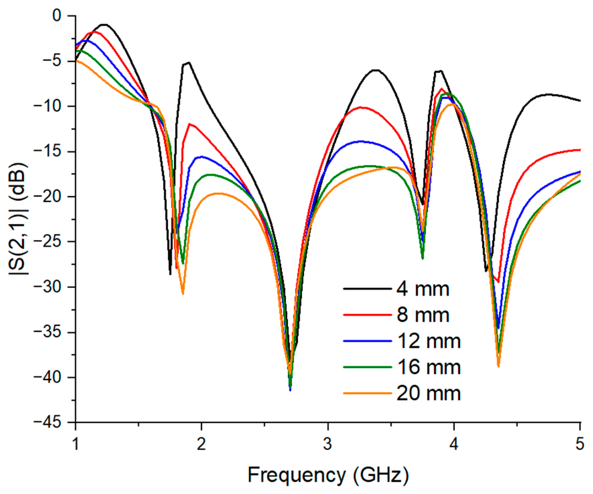
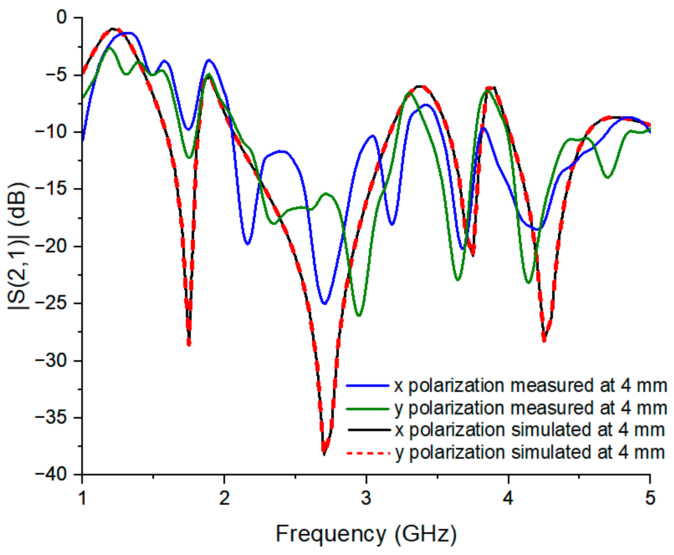
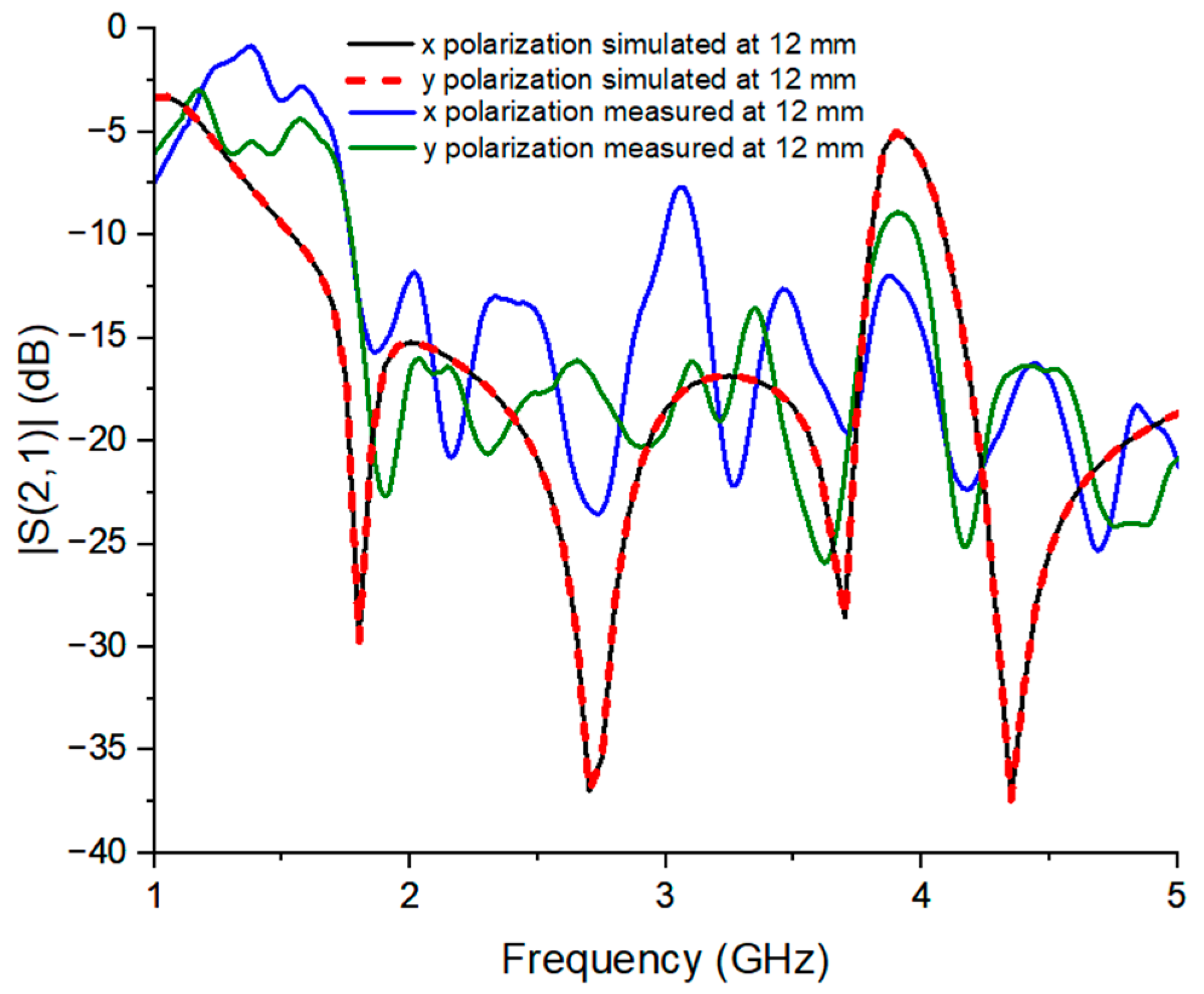
  • Dual-band operation with bandwidths that depend on the spacing between the FSS boards, one with a 1.2 GHz bandwidth in the 2 to 3.2 GHz range, for a spacing equal to 4 mm, and another with a 2 GHz bandwidth in the range from 1.8 to 3.8 GHz, for a spacing of 12 mm.
  • Use of the negative geometry of a matryoshka geometry and its effect with the matryoshka in cascade.

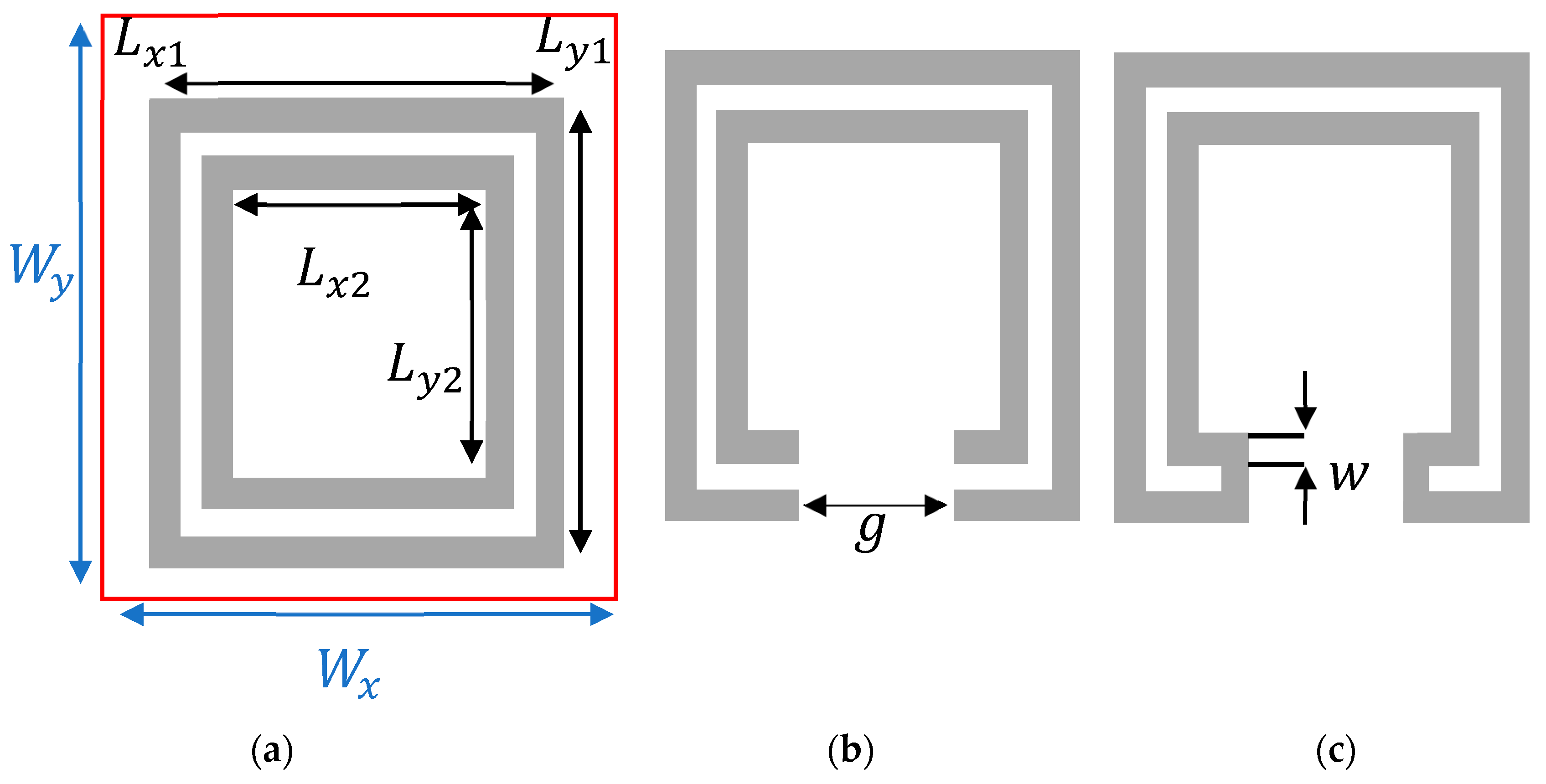
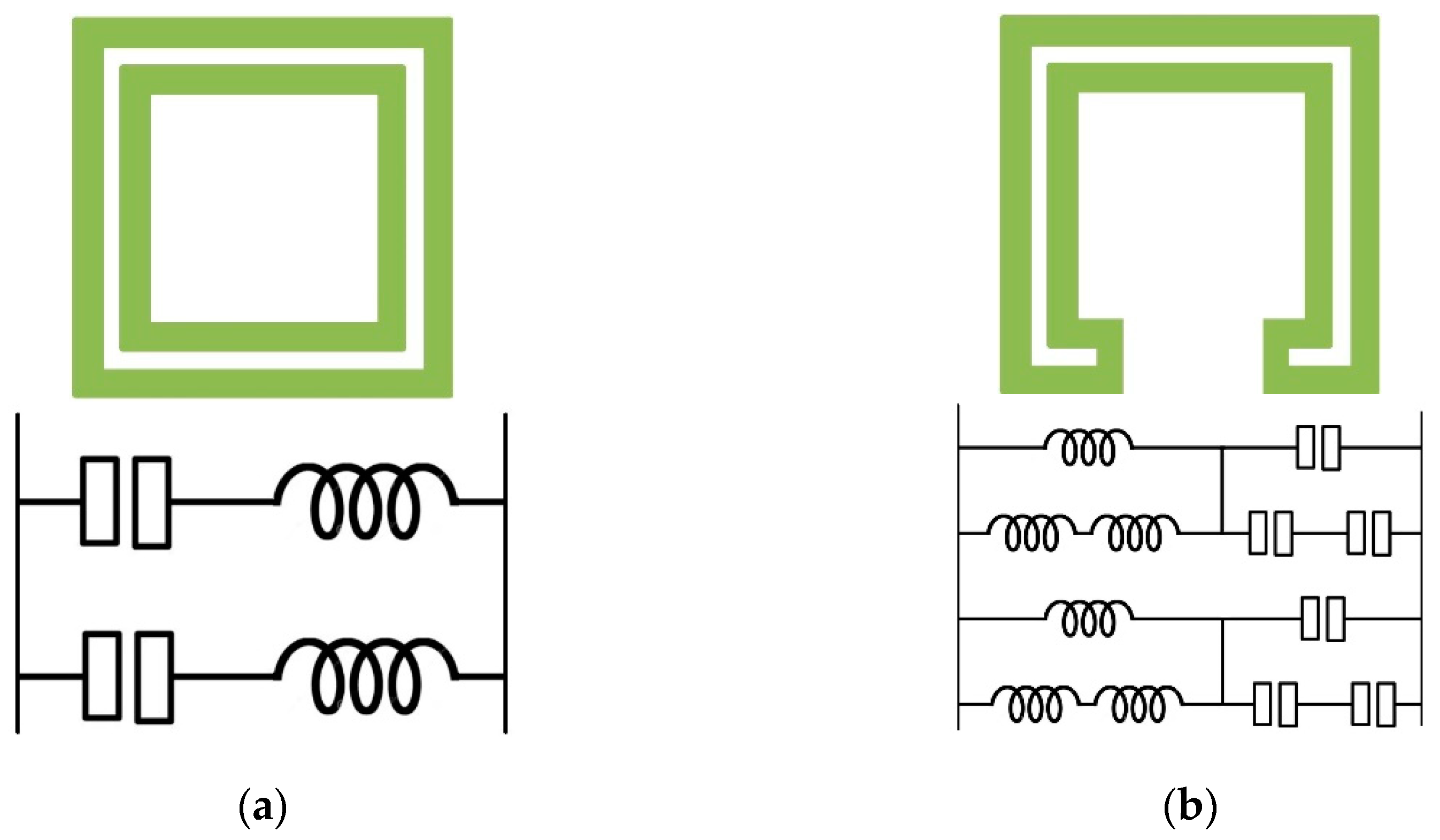
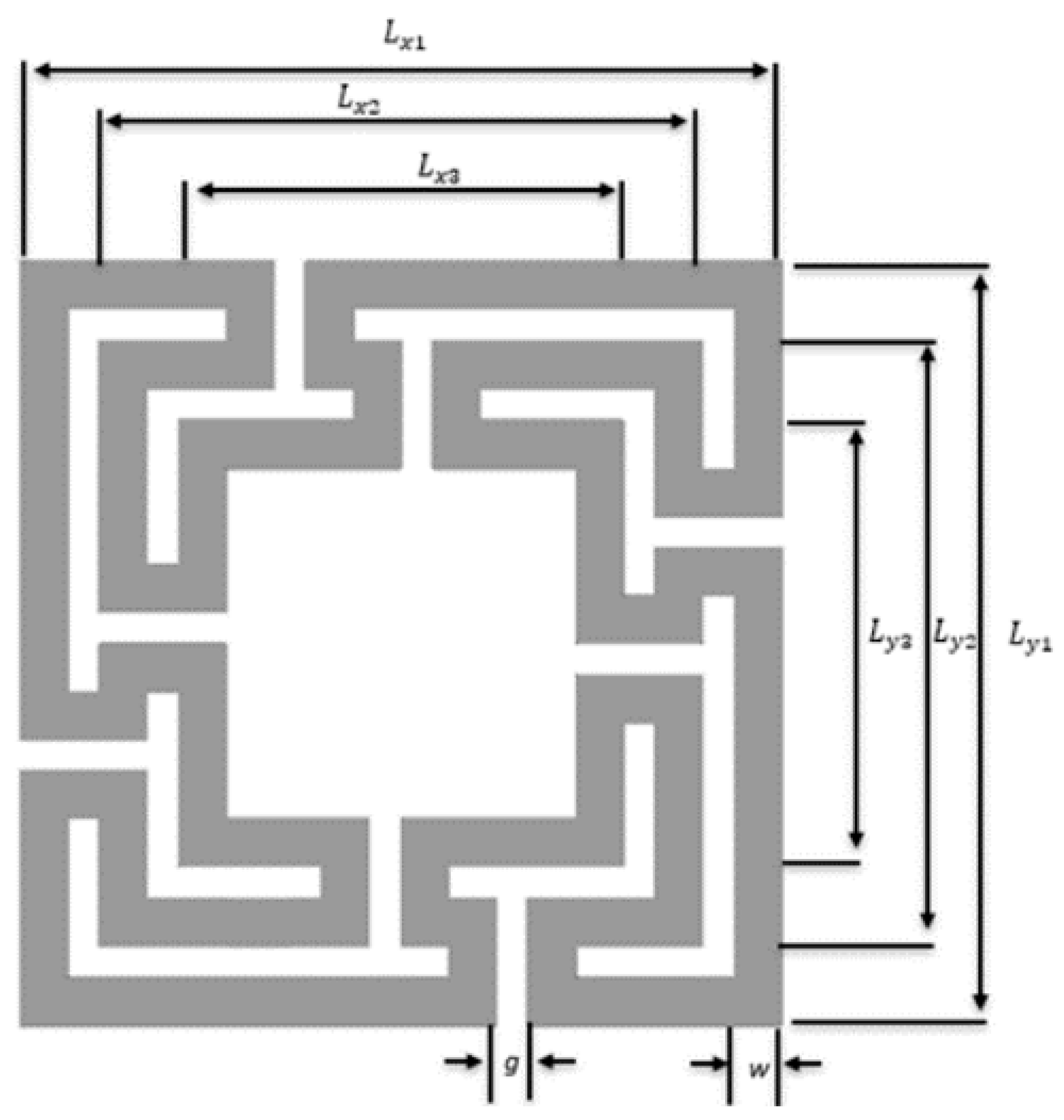
2. Proposed Matryoshka Design

The matryoshka geometry is inspired by the Russian dolls of the same name, in which a larger doll contains a smaller doll, which contains another smaller doll, and so on, but all occupying only the volume of the larger doll [38]. Its design starts with concentric rings with width w and lengths L x 1 and L y 1 for the outer ring and L x 2 and L y 2 for the inner ring on a unit cell with length W x and W y . Then, the concentric rings receive slits of length g at the same point and are connected to each other with two strips of the same width w as the rest of the two rings, making one continuous line through the whole geometry, as shown in Figure 2.
As the rings are interconnected, the effective length of the matryoshka ring increases without increasing the occupied area, limited to the area of the outermost concentric ring, presenting features like miniaturization and multiband operation. This geometry is polarization-dependent, with the connecting part being displayed only on the right side of the design.
For an equivalence in circuits, the base of the concentric rings is used, such as a pair of square rings, so the equivalent circuit behaves as a dual circuit of inductors and capacitors, as shown in Figure 3a, with each square ring being equivalent to one inductor and one capacitor in series being presented in parallel because of their position as concentric squares. By connecting these two rings, it is possible to obtain a matryoshka geometry. The connections between them introduce more inductor and capacitor elements both in series and in parallel, as shown in Figure 3b. In more complex geometries with more rings and connections, such as examples with independent polarization, numerical methods are needed to generate an accurate equivalent circuit [38,39,40].
The matryoshka geometry [40] was the base for the geometry developed in this paper, with independence of polarization and a more complex design.
This paper presents the use of the geometry displayed in Figure 4 for one of the FSS and its negative equivalent for another. This modified matryoshka geometry has connections between the rings on each side of the squares, making it a more symmetric design.
The connections between the three rings on each side make the geometry horizontally and vertically symmetric and independent of polarization. The dimensions used in the project are shown in Table 3. Usually, L x 1 = L y 1 = L 1 for square rings. Hence, L x i = L y i = L i with i = 1 ,   2 ,   3 .
As a first approach, the matryoshka geometry’s resonant frequencies ( f r e s 1 and f r e s 2 ) can be estimated by [20,21]
f r e s 1 G H z = 0.3 L e f 1 ε r e f ,
and
f r e s 2 G H z = 0.3 L e f 2 2 ε r e f ,
with
L e f 1 = 3 ( L 1 2 w 1 ) + 2 ( L 2 2 w 2 ) + 3 ( L 3 2 w 3 ) ,
L e f 2 = 3 L 1 + 2 L 2 + 3 L 3
and
ε r e f = ε r e f C P W + 1 2 .
The variables L e f 1 , L e f 2 , and L e f 3 are the effective length of each ring used to calculate the resonant frequencies and the variables ε r e f and ε r e f C P W are the effective relative dielectric constant for the microstrip and for a coplanar waveguide, respectively. The latter is obtained by using numerical integration software like APPCad [42] with the values of the dimensions and materials used.
The FSSs proposed in this paper were manufactured using sticker printing, in which an array of the unit cells with the designed geometry is printed into a metallic surface of the FR-4 substrate plate and then corroded by iron perchloride. The iron perchloride removes the metallic surface from the plate, except on the parts covered by the sticker printing. The FSSs are presented in Figure 5 and contain 8 × 8 cells. For the cascaded configuration, the FSS layers are positioned on top of each other, as shown in Figure 6. The layers are spaced by acrylic supports that make it possible to adjust the g spacing between them, as shown in Figure 7. It is possible to see that the second FSS is the negative geometry of the first FSS; thus, the metallic surfaces of the two layers do not overlap when cascaded. The acrylic supports and FSSs are fixated by two iron screws of 1 cm diameter and 25 cm length and attached to the measurement window. The screws press the FSS and support so there is no additional gap between layers, except the spacing provided by the acrylic support. This fixation method also aligns the unit cells of both FSSs.

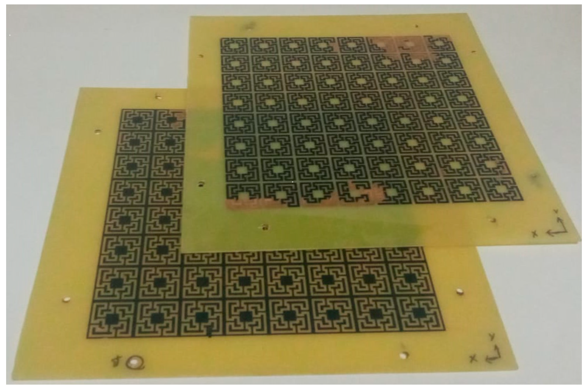
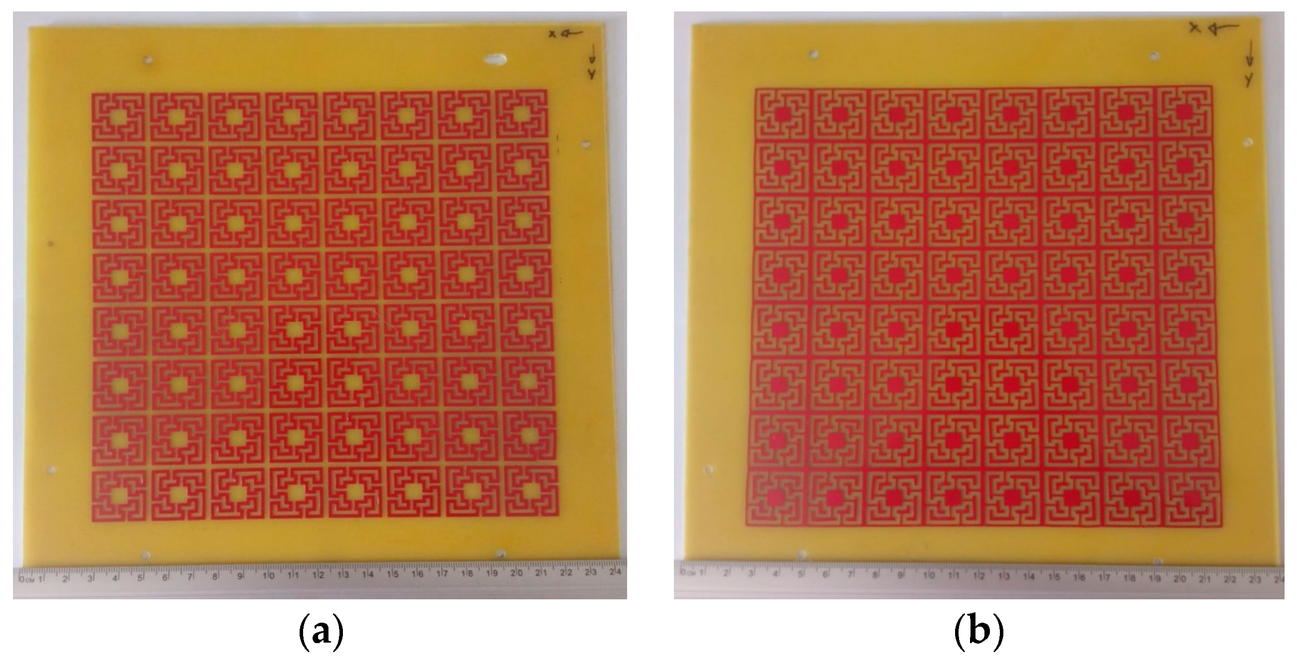
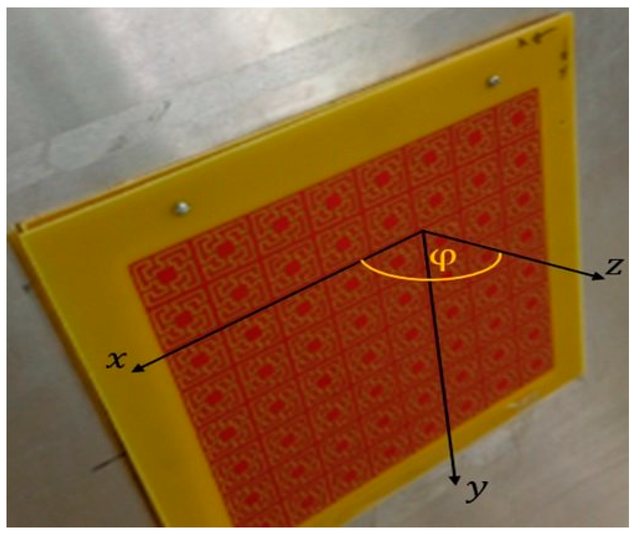
3. Measurement Setup

With the FSSs manufactured and prepared, the setup for the experimental measurements of FSSs used the microwave measurement laboratory of the Telecommunications and Applied Electromagnetism Group of the Federal Institute of Education of Paraiba (GTEMA-IFPB), shown in Figure 8, with a two-port VNA E5071C network analyzer and Pasternack Enterprise PE9859-20 horn antenna.
FSSs were placed on acrylic holders measuring 20 cm2 with different thicknesses of from 2 mm, 3 mm, and 5 mm. They were placed in a measurement window to minimize reflection and deflection issues. The measurement window is made of an 80 × 60 cm² plane of aluminum with a 20 × 20 cm² vent in the middle with small holes to screw and secure the FSS and acrylic holders, allowing the signal to travel between a horn antenna placed 1.5 m from the measurement window to the other side, passing through the vent with the FSS. Other signals that hit the measurement window are deflected, not reaching the other horn antenna, also placed 1.5 m from the measurement window. With this device, it is possible to analyze the response of the FSS to a planar incident wave polarization, as well as to its incidence angle φ, as shown in Figure 9, in which the window is horizontally rotated according to the desired angle. Measurements of the frequency response of the cascaded FSSs were conducted separately, with the band-reject FSS superimposed and with different gaps between the FSSs, as shown in Figure 10. Finally, reference measurements of the environment were conducted to analyze the results.
The method of each measurement was repeated so that the FSS frequency response was measured at angles from 0 to 45° in 15° intervals to analyze the stability of the frequency response in relation to the angle variation. The plates were also measured in horizontal x and vertical y polarizations of the transmitting antenna and finally, in the case of the cascaded FSS configuration, measurements were conducted with the spacing between plates varying incrementally from 3 mm to 20 mm to analyze the behavior of the frequency response.
It is possible to minimize the influence of external factors, such as environmental conditions or manufacturing imperfections. A printing machine is used to manufacture and affix the printed design on the plate to avoid imperfections in the unit cells. To minimize environmental factors—such as reflections and diffractions of the signal waves on objects around the setup, the interference of external signals that reach the room, the edge effect when the signal waves hit the corners of the FSS, and other influences of the environment—reference measurements are used for the experimental results. These reference measurements are obtained with a setup without any FSS in the measurement window, and this way, it is possible to measure the environmental influence on the setup. This procedure is repeated for each incident angle and then used to normalize the frequency responses presented in this article.

4. Results Analysis

The simulated results were obtained with the commercial software Ansys DesignerTM for a FR-4 substrate with dielectric constant ε r = 4.4 and thickness h = 1.6 mm, using the High-Frequency Simulation Software (HFSS) mode [43].
A plane wave source was considered with post-processing settings of 1 V for both horizontal and vertical polarizations and the infinite array setup with boundaries in the dimensions of the unit cell, W x and W y , shown in Table 3. These settings were made to infinitely repeat the simulation of the geometry traced on those boundaries.
The frequency sweep had a linear step distribution from 0 GHz to 10 GHz with a step size of 0.05 GHz. Then, this was adjusted for a 0.01 GHz step size ranging from 1 GHz to 5 GHz.

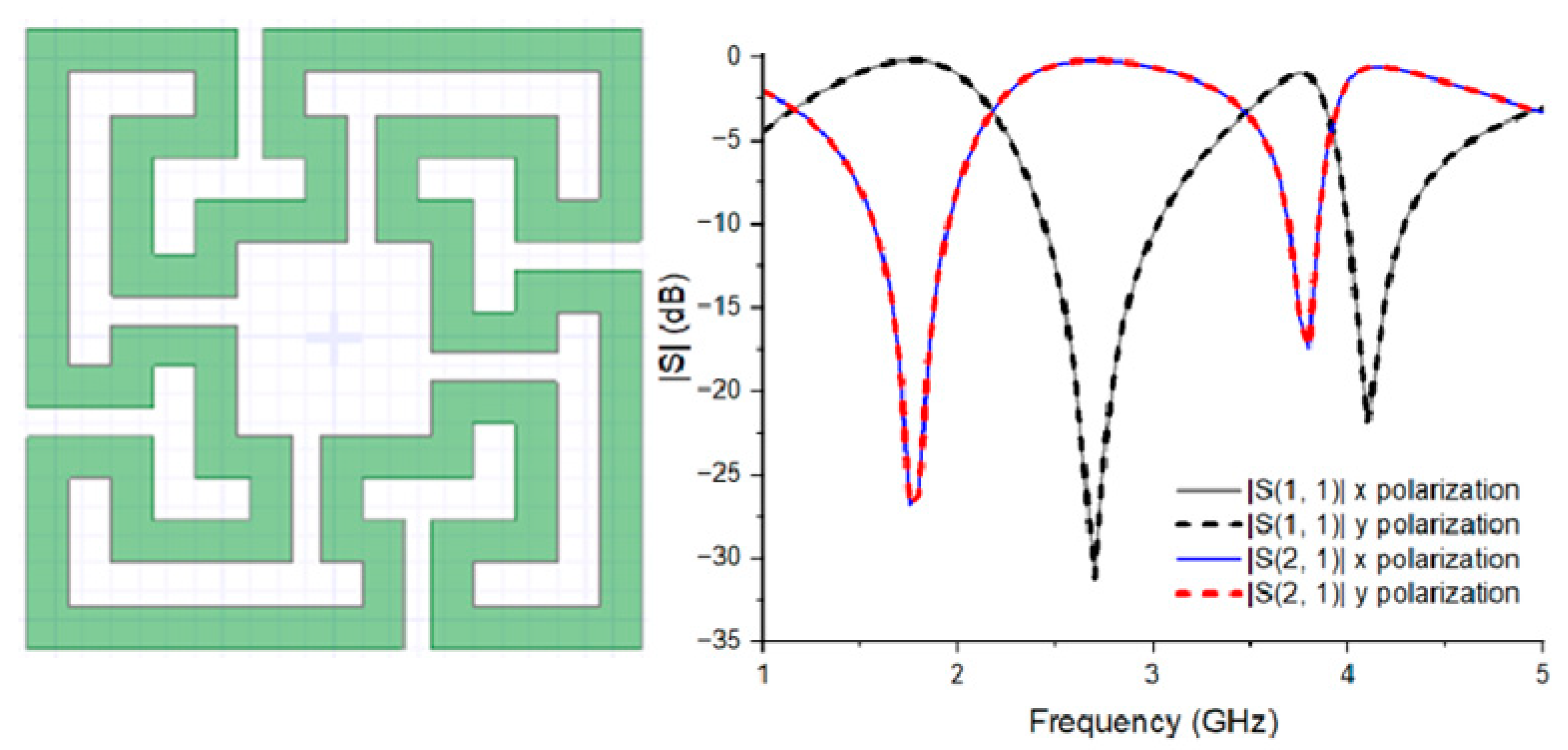
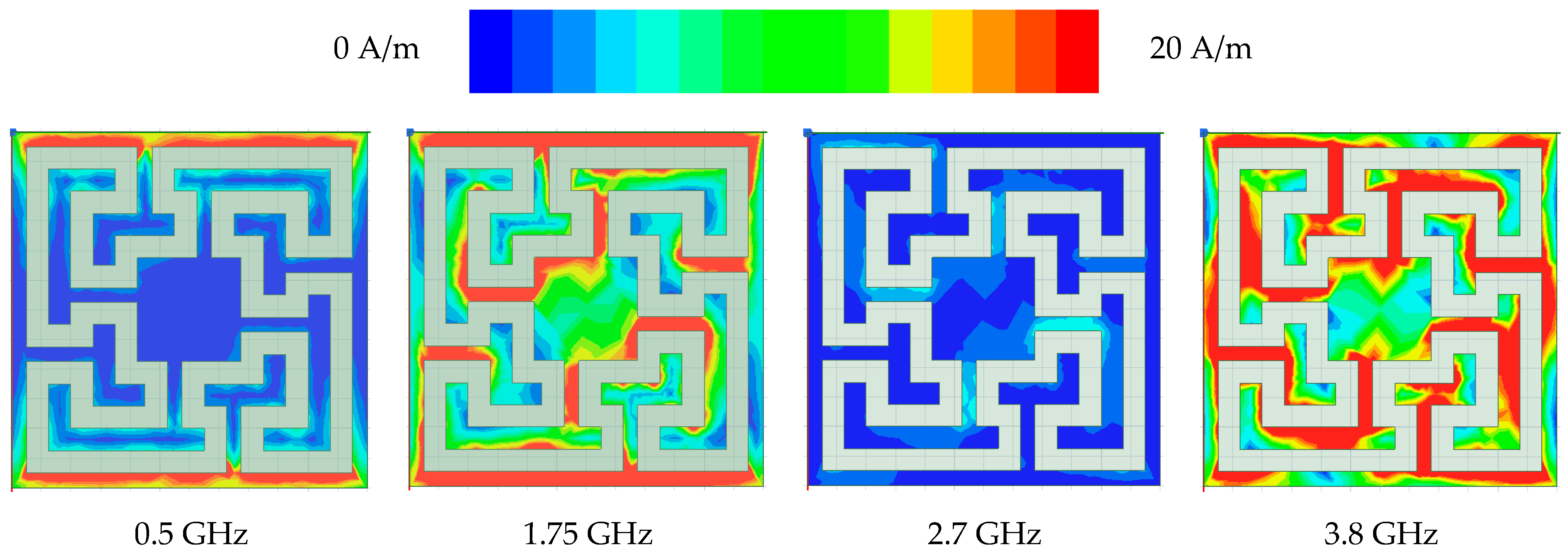
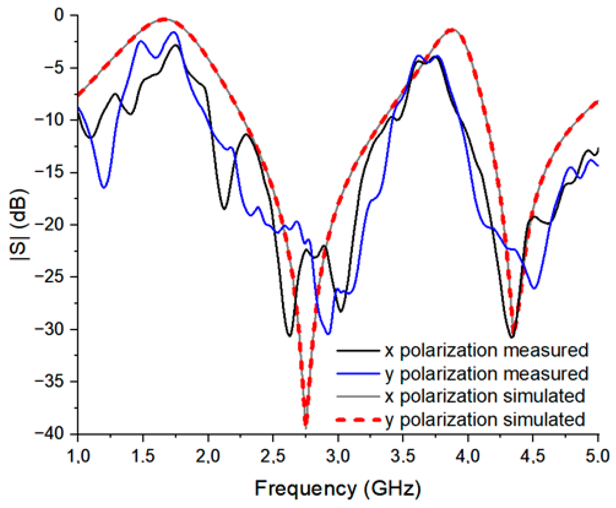
4.1. Single-Layer FSS
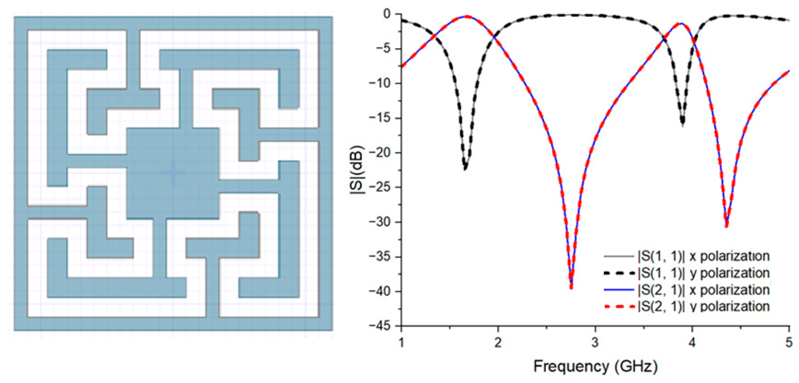
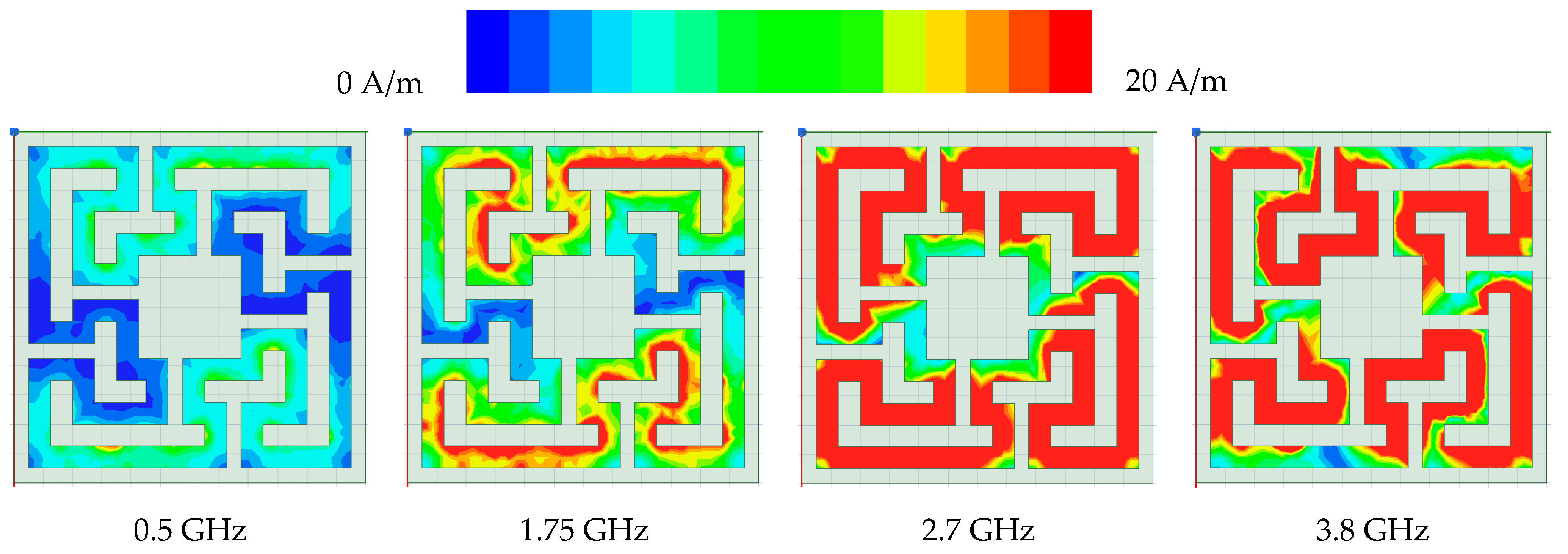
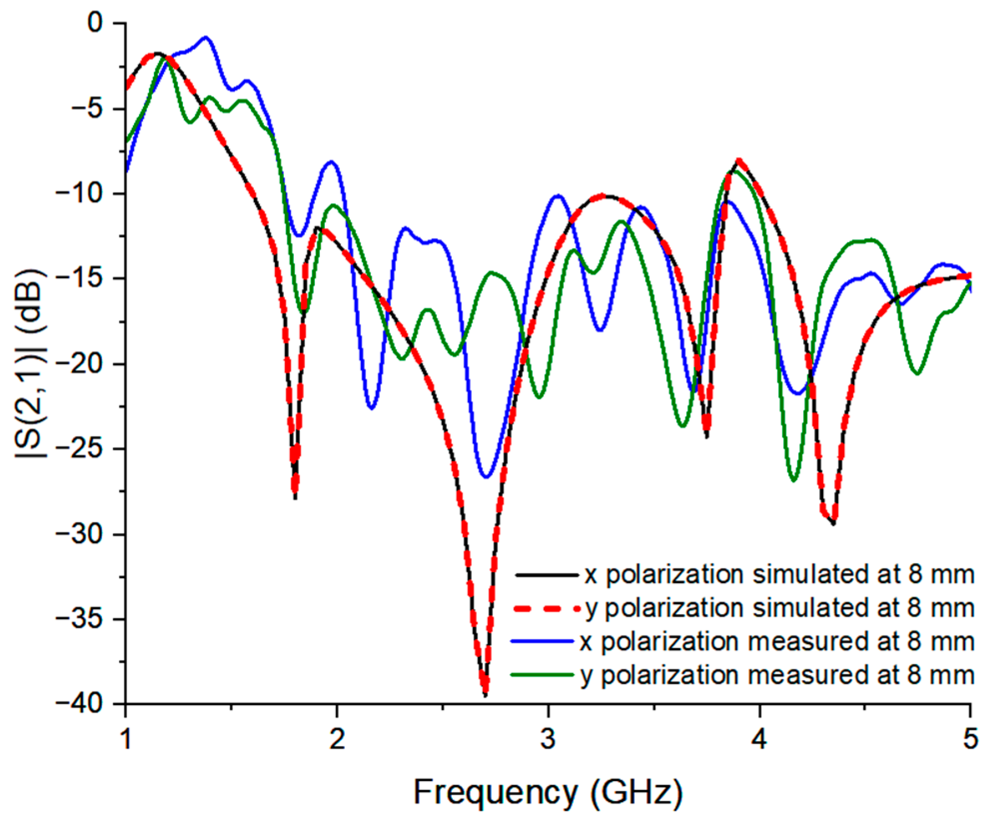
The curves shown in Figure 11 and Figure 12 were obtained considering horizontal and vertical polarizations for the incident wave. They show the simulated frequency response of the FSS in terms of the modulus of the parameter S, both when transmitting, | S 2 , 1 | , and reflecting, | S 1 , 1 | , the incident plane wave.
As expected, due to the matryoshka geometry being symmetrical on all sides, perfectly identical results were obtained in both polarizations, where the signal transmitted in vertical polarization is identical to the signal transmitted in horizontal polarization
Also, as expected, when implementing the negative of a band-stop matryoshka geometry, we have a band-pass matryoshka geometry with an inverted frequency response, in which the reflected signal of the band-pass structure presents the same resonant frequencies as the signal transmitted from the band-stop structure. However, for this analysis, we consider its lowest points of | S 2 , 1 | as resonance frequencies so that it is possible to observe their effects in the cascaded structure.
The resonant frequencies of the matryoshka geometry FSS were 1.75 GHz and 3.8 GHz, as shown at the lower points of the blue and red lines in Figure 11. Meanwhile, the FSS with negative matryoshka geometry, although having the same resonance frequencies of 1.75 GHz and 3.8 GHz at their peaks, shows its lowest frequencies at 2.75 GHz and 4.15 GHz, as shown in the red and blue lines of Figure 12.
It is important to note that although the geometry in Figure 12 is the exact negative of the geometry in Figure 11, the frequency responses of the FSSs are not exactly reversed, even in the simulation. In the simulation, all the unit cells are identical and without any manufacturing errors, but the FSSs behave as different types of filters.
The matryoshka geometry FSS behaves as a band-reject filter, blocking frequencies within the bandwidth range and letting frequencies outside the bandwidth range pass through. In the resonance frequency, the lower the value of the frequency response, the better the band-reject filter blocks the signal.
The negative of the matryoshka FSS behaves as a band-pass filter, passing signal waves on frequencies within the bandwidth range and attenuating frequencies outside that bandwidth range. For the resonance frequency, the closer to 0 dB the frequency response is, the better the FSS lets the signal wave pass through. This is why, in Figure 11, the frequency responses presented lower values at 1.75 GHz and 3.8 GHz compared with Figure 12.
A simulation was carried out of the electric current distribution for both FSS layers. The FSSs present different electric current paths in the metallic surface due to electromagnetic coupling between the geometry trails. The FSS geometry on the metallic surface generates a resonant effect that results in microwave trapping and absorption. The attenuation of EM waves is generated as the electric field interacts with the electrons and induces currents due to the presence of conductive metal.
In Figure 13 and Figure 14, we observe the electric current distribution in the single layers. For a band-pass FSS, if there is current excitation in the unit cell, the signal passes through the FSS at a chosen frequency. If the unit cell is excited by an electric current, then the FSS reflects the signal wave. The reverse is true for a band-reject FSS when no excitement in the unit cell lets the signal pass through, while a current excitation causes the FSS to reflect the signal at a chosen frequency.
Figure 13 shows a 0.5 GHz frequency electric current distribution for which the signal is blocked by the FSS due to insufficient current excitation.
One observes in Figure 13 that at the frequency of 1.75 GHz, which is the first resonance frequency, there is enough electric current through all the rings of the geometry to allow the signal wave to pass. This is the frequency in Figure 12 at which | S 2 , 1 | attains −0.37 dB. The incident signal wave also passes through the FSS at 3.8 GHz in Figure 13, which is the second resonance frequency. At 2.7 GHz in Figure 13, it is possible to see that the electric current in the unit cell attains the lowest intensity, so the signal wave cannot pass through the FSS, which is the reason why the lowest point in the frequency response is attained in Figure 12.
The electric current distribution for reject-band FSS is shown in Figure 14. At 0.5 GHz, the unit cell is not sufficiently excited by the electric current, allowing the signal wave to pass through the FSS. At the first resonance frequency in Figure 14, 1.75 GHz, a high electric current density is observed in the outer ring of the unit cell, contributing to the FSS reflecting the signal wave. However, at 2.7 GHz, even with a high electric current density in the outer ring of the unit cell, the signal wave passes through the FSS. That happens because the inner ring has a low current density and a frequency higher than the one in the previous example. The signal wave will only be reflected when the inner ring has a sufficient electric current density, as seen at 3.8 GHz in Figure 14.
The results below were obtained by individually measuring the signals that interacted with the FSSs and the horn antennas. They were normalized by the reference measurements to minimize the losses caused by the environment.
Figure 15 and Figure 16 show the results obtained with the measurement for an FSS with matryoshka geometry at different inclinations, for different values of the angle φ and polarizations. The signal loss is greater for angular inclinations close to 90°, when the situation is equivalent to a measurement without FSS since, in this case, the incident plane wavefront is perpendicular to the FSS plate.
Analyzing the frequency response of the FSS, it can be noted that the greater the horizontal angular inclination of the measurement window regarding the incident plane wavefront, the greater the displacement of the curves to the left in relation to the frequency response with a horizontal inclination of 0°, where the FSS plate is perpendicular to the incident wavefront. It can also be noted that, although the frequency responses for the two polarizations of the incident wave are not identical—as expected due to the symmetric matryoshka geometry—it is possible to identify resonance frequencies at 1.8 GHz and 3.6 GHz at 0°, both for x and y polarizations, as shown in the black trace of Figure 15 and Figure 16.
When the wavefront incidence angles are considered, one can observe that the first resonance frequency varies from 1.81 GHz for y polarization at 30°, as shown in the blue trace of Figure 15, to 1.88 GHz for x polarization at 45°, as shown in the green trace of Figure 16. Meanwhile, the second resonance frequency varies from 3.65 GHz for y polarization at 30°, in the blue trace of Figure 16, to 3.70 GHz for x polarization at 45°, in the green trace of Figure 15.
The frequency response that presents the maximum resonance frequency displacement was obtained for an incidence angle of 45° for y polarization, in the green trace of Figure 16. Despite the first and second resonant frequencies being 1.74 GHz and 3.62 GHz, both close the frequency response with an inclination angle equal to 0° with 1.8 GHz and 3.6 GHz, the lower frequencies present different behavior regarding the other traces presented in Figure 16, showing a distortion in the bandwidth below −10 dB ranging from 1.2 GHz to 2.2 GHz. Comparing these results, we observe a difference smaller than 0.02 for both inclinations of 15° and 30° and a higher 0.06 GHz difference when the inclination is at 45°. Also, except for the inclination of 45°, all others have a range of 1.63 GHz to 2.0 GHz below −10 dB. Those resonance frequencies and bandwidths are considered influences on the FSS in cascade frequencies together with the other FSS resonance frequencies.
The experimental frequency responses of the negative matryoshka geometry FSS, acting as a band-pass filter, are shown in Figure 17 and Figure 18.
The frequency responses of the FSS with negative matryoshka geometry were more distinct in relation to the simulated results of the resonance frequencies for the y polarization of the transmitting signal, as shown in Figure 18. A resonance frequency around 1.2 GHz was present, similar to the x polarization at 45° of the matryoshka geometry, seen in the green trace of Figure 16. This disparity may be caused by the horn antenna’s performance for signals with frequencies near the edge of its operating range.
The resonance frequencies of the FSS with negative matryoshka geometry for x polarization on the incidence angle φ equal to 0°, as shown in the black trace of Figure 18, were 2.6 GHz and 4.3 GHz, at which the transmission coefficient attained the lowest value. For y polarization on φ equal to 0°, as shown in the black trace of Figure 18, these resonance frequencies were 2.8 GHz and 4.4 GHz. For both polarizations, the FSS behavior remained as a band-pass in the range from 3.35 GHz to 4.15 GHz around the 3.7 GHz frequency.
When the incidence angle, φ, of the measurement window was considered higher than 0°, the first resonance frequency of the FSS remained stable for both horizontal and vertical polarizations, with the largest shifts of 0.06 GHz at 15° for x polarization, as shown in the red trace of Figure 17. When analyzing the second resonance frequency, the higher shift for the x polarization was 0.2 GHz with the incidence angle φ equal to 45°, as shown in the green trace of Figure 17, and 0.3 GHz for the y polarization, the same incidence angle, shown in the green trace of Figure 18. Comparing the range below −10 dB, once again all the other inclinations except for 45° share a range of 2.0 GHz to 3.3 GHz

4.2. Cascaded FSS

The characterization of the cascaded FSS was conducted following the same procedures as the previous FSSs. Figure 19 shows the frequency response graph of a cascaded FSS with two layers aligned with different spacing between them, incrementing millimeter by millimeter. It is possible to see that as the spacing increases, the bandwidth uniformly increases between 1.7 GHz and 3.8 GHz, reaching up to 2 GHz.
The simulated frequency response, in terms of the modulus of the transmitting parameter S 2 , 1 as a function of the incident wave frequency, presents the highest bandwidth equal to 2.1 GHz at spacings of 18 mm, 19 mm, and 20 mm between the two parallel layers, while the lowest bandwidth equal to 1.1 GHz occurs for a spacing equal to 4 mm. The increase in bandwidth was saturated for a spacing of around 18 mm for the highest bandwidth and 4 mm for the lowest bandwidth.
An analysis was conducted for the electrical current distribution of the cascaded FSS, presented in Figure 20. At 0.5 GHz, we observe the band-reject allowing the wave signal to pass through the first layer, but the band-pass reflects the signal due to the low electric current distribution, preventing the wave signal from reaching the receiving antenna. At 1.75 GHz in Figure 20, the band-reject has a high electrical current distribution throughout the unit cell and the FSS reflects the signal before reaching the second layer. That is why at this frequency in the blue line in the frequency response of Figure 19, we can observe that the 1.75 GHz is below −10 dB. At the frequency of 2.7 GHz in Figure 20, the current distribution in the band-reject seems to be sufficient, but as previously in Figure 14, the inner ring has a low current density through which the wave signal can pass from the first layer. However, it is prevented by the second layer due to a low electric current distribution in the band-pass. The last frequency analyzed in Figure 20 was 3.8 GHz, where despite the second layer with the band-pass having a high enough electric current distribution to allow the wave signal to pass through, the first layer with the band-reject is reflecting with the high electric current density in the inner ring.
The experimental results, on the other hand, did not show such a uniform pattern in the frequency response. In Figure 21, frequency response curves are presented for spacing between the parallel FSSs varying from 4 to 4 mm for the x polarization.
The same procedure was repeated for y polarization to generate Figure 22. From these results, it is possible to see that the measured frequency responses have a pattern of shifting the resonance frequency relative to the variation in the spacing between the FSS layers.
In the frequency response measured for x polarization, it only varies from 2 GHz to 3.2 GHz for 4 mm and from 1.75 GHz to 3 GHz for 12 mm and higher, as shown in Figure 21. In contrast, for y polarization, there is a 1.2 GHz bandwidth in the 2 to 3.2 GHz range for a spacing equal to 4 mm, and another with a 2 GHz bandwidth in the range from 1.78 to 3.82 GHz for spacings of 12 mm and higher, as shown in Figure 22.
The influence of the wavefront incidence angle, φ, can also be analyzed by observing Figure 23 and Figure 24. These figures show the experimental frequency response of the cascaded FSS, in terms of | S 2 , 1 | , for different values of the wavefront incidence angle φ, y polarization, and two different values of the spacing between the layers, equal to 4 mm and 12 mm, respectively.
By analyzing the frequency responses in terms of | S 2 , 1 | for the wavefront incidence angle φ equal to 15°, corresponding to the blue trace in Figure 23 and Figure 24, one can see that the higher deviation to the black trace, corresponding to the incidence angle equal to 0°, occurs in the range from 2 GHz to 3.4 GHz. For both polarizations, the frequency responses present a similar bandwidth, below −10 dB, for an incidence angle equal to 0°. The same can be said for the incidence angle equal to 30°, corresponding to blue curves in Figure 23 and Figure 24, with a slightly larger deviation but still maintaining a similar bandwidth for the incidence angle equal to 0°.
For an incidence angle equal to 45°, shown in red traces of Figure 23 and Figure 24, there is a noticeable difference in the bandwidths observed in the frequency responses for polarizations x and y , regarding the frequency response obtained for an incidence angle equal to 0°. For x polarization, the bandwidth changes from the range 2~3.2 GHz, for an incidence angle equal to 0° and gap of 4 mm between the FSS layers, to the range 2~3.7 GHz and an incidence angle equal to 45°. For y polarization, the bandwidth changes from the range 1.78~3.82 GHz for an incidence angle equal to 0° to the range 2~5 GHz for an incidence angle equal to 45°.
Plotting the samples of frequency response obtained by simulation and experimental measurement of each single layer of the FSS for an incidence angle equal to 0°, one obtains the curves shown in Figure 25 and Figure 26.
As expected, the simulated results are not identical to the experimental ones due to external factors such as environmental characteristics and non-ideal conditions of FSS manufacturing on the experimental side. On the other hand, ideal considerations, like infinite plane on the simulation side, are also taken into account. It is possible to reduce the influence of such factors by considering a reference measurement campaign performed on the setup. The biggest difference was the patterned decay of the range on the border between 1.8 GHz to 2 GHz. Although the behavior in experimental frequency response was not as variable as the simulation, the measured results still had visible differences for each spacing and kept their similarities with what was expected in the simulation.

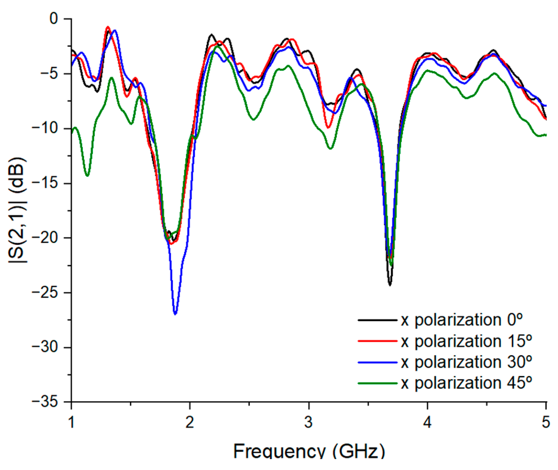
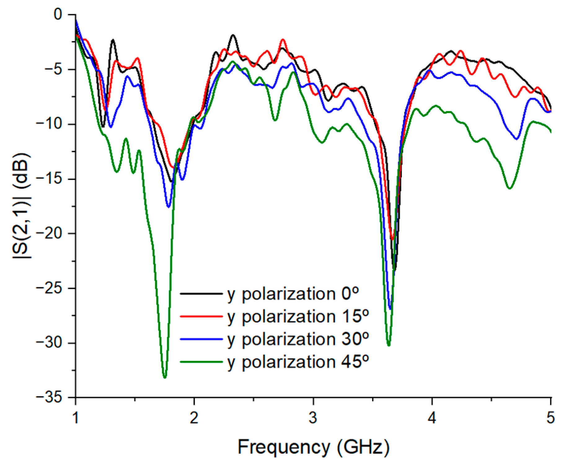
4.3. Comparisons of Experimental and Simulated Results

It was expected that the experimental results would not be identical to the simulated ones due to many factors. There could be external factors in the experiment, such as the environment or the manufacturing process. There were also ideal factors in the simulation, such as the infinite plane and an exact source wave. Simulations do not consider that even a directive antenna, like the horn antenna used in setup, can suffer diffractions, reflections, and other effects when the signal wave interacts with the edges of objects like the measurement window or the surrounding environment.
In the analysis of the measured and simulated results, Figure 25 presents the frequency results of the simulated and measured x and y polarizations of the band-reject FSS with matryoshka geometry, and Figure 26 shows the frequency results of the band-pass FSS with the inverse matryoshka geometry with the simulated and measured x and y polarizations.
By analyzing Figure 25, it was possible to see the similarities and discrepancies between the measured and simulated results of the reject-band FSS. The first simulated resonance frequency is at 1.75 GHz for both polarizations, and the measurements are at 1.78 and 1.77 GHz for the x and y polarizations, respectively. Comparing these values, there is a displacement of 0.03 GHz from the simulations to the measurements. When the bandwidth of the first resonance was analyzed, the simulated frequency results presented a bandwidth from 1.60 GHz to 1.95 GHz, while the bandwidth in measured frequency results ranged from 1.64 GHz to 1.99 GHz. These bandwidths from simulated and measured results together presented an overlap of more than 77%.
The highest discrepancy in Figure 25 was the bandwidth around the second resonance frequency. The simulation presented a resonance frequency at 3.8 GHz, and both x and y polarizations in the measured results showed the second resonance frequency at 3.6 GHz. Those frequencies presented a discrepancy of 0.2 GHz as well as an overlap of 60% between the bandwidths around them. Such discrepancies can occur due to expected differences between the simulations and measurements, such as the FSS not being infinite or the plane wave not being ideal.
In Figure 26, we observe some discrepancies when comparing simulated and measured results. The first peak, around 1.75 GHz, remained the same for both the measured and simulated results, but the second resonance frequency was shifted by 0.05 GHz, with the simulation frequency being 3.8 GHz and the measurement frequency being 3.75 GHz.
The bandwidth below −10 dB in the frequency results in Figure 26 showed an interesting behavior at both resonance frequencies. The measured bandwidths started before and ended after the ones in the simulated result, thus presenting a larger range than expected from simulations. The bandwidth around the first resonance frequency in the measured results was from 2.0 GHz to 3.5 GHz, while in the simulation, it ranged from 2.3 GHz up to 3.5 GHz, a gain of 0.3 GHz. The bandwidth around the second resonance frequency in the simulation has a section from 4.1 GHz to 4.8 GHz, while the measurement goes from 3.9 GHz to higher than 5 GHz. The comparisons between the measured and simulated results of the band-pass FSS were more in agreement than those of the band-reject FSS, and the additional bandwidth was a distinct influence on the cascaded FSS.
Analyzing the frequency responses of a single layer FSS, shown in Figure 25 and Figure 26, it is possible to see that their resonance frequencies are present in the frequency response of the cascaded FSS, as shown in Figure 27, Figure 28 and Figure 29 for different spacings between the layers, contributing to a wider bandwidth. The simulated and experimental frequency responses of cascaded FSS comparison can be analyzed by observing Figure 27, Figure 28 and Figure 29 for the gaps of 4 mm, 8 mm, and 12 mm between the layers, respectively.
In Figure 27, we observe that the bandwidths below −10 dB align from 2.0 GHz to 3.2 GHz between the measured and simulated results, allowing a large bandwidth of 1.2 GHz with 4 mm between the layers. Although the measured results did not reach the simulation intensity peak at −40 dB, this was expected since the simulation has ideal values and an infinite plane. The frequency response values in the range from 2.0 GHz to 3.2 GHz remained around −20 dB for more than half of the frequencies.
Observing Figure 28, the frequency responses between 1.8 GHz and 2 GHz for the x polarization are close to −10 dB, especially for the peak at 2.5 GHz. This makes it difficult to determine the bandwidths. The y polarization starts to show the possibility of a 2 GHz range, but because its peaks are too low, using this spacing would not present a stable bandwidth.
In Figure 29, there is a clear ultra-bandwidth for the y polarization, with the range between 1.8 GHz and 3.8 GHz being below −10 dB and up to −15 dB at most of its frequencies. The range from 1.8 GHz to 3.0 GHz in the x polarization is also more distinct because there is a shift of about −5 dB between the 8 mm and 12 mm spacings, which made 2 GHz UWB possible.
Compared to the simulated results, the bandwidth below −10 dB in the measured results was expected to start at 1.6 GHz. This shift can be explained by analyzing the responses of single-layer FSSs, where the first resonance frequencies were shifted to the right at the first resonance. There were discrepancies, and although the cascaded FSS maintains similar resonance frequencies in experimental and simulated frequency responses, the measured values of |S(2,1)| at these frequencies do not show a decay as sharp as the simulated values. These differences in intensity are due to the fact that the ANSYS simulation uses numerical methods and does not take into account factors such as antenna limits, connector and cable wear, and edge effects.
Further experiments and simulations showed that most of the discrepancies were due to the alignment of the FSSs. By creating overlaps between the geometries of the layers, the resonance frequencies affected each other and shifted from the intended ones. Even with the non-ideal parallelism of the layers, it was possible to obtain a bandwidth of 2 GHz.

5. Conclusions

The purpose of this paper is to present a cascaded FSS with two layers, one with matryoshka geometry and the other with its inverse matryoshka geometry, to extend the operational bandwidth to 2 GHz, in the range from 1.8 GHz to 3.8 GHz with a gap of 12 mm between layers and 1.2 GHz in the range from 2 GHz to 3.2 GHz with a gap of 4 mm between the layers, making an ultra-wideband possible. This allows for a bandwidth that includes both 2.4 GHz and 3.65 GHz WLAN frequencies, as well as part of the 2 GHz band.
The proposed cascaded FSSs were evaluated by simulated and measured results. It was shown that matryoshka geometry has advantages in comparison with other designs. The resonance frequencies were analyzed, revealing that the matryoshka geometry FSS behaved as a band-pass filter while its negative behaved as a band-reject one. Their different frequency responses and how complementary they were allowed for a larger bandwidth with the cascaded FSS layers.
Cascaded FSSs with different spacing between the layers were characterized. The simulated frequency responses for each gap followed a pattern that reached a bandwidth of 2 GHz when the spacing was 12 mm or higher. Two square FSSs with an area of 24 mm2 and 8 × 8 unit cells were characterized, and their numerical results were analyzed according to the theoretical equations of the geometries. The cascaded matryoshka geometry showed to have a good coupling between the two layers, with the resonance frequencies complementing each other, making it possible to obtain a bandwidth greater than that of single layers.
The results were analyzed for different polarizations as well as different incidence angles regarding the transmitting antenna opening plane. The proposed design showed the stability of the matryoshka geometry and how it was maintained even in a cascaded configuration. By maintaining the bandwidth for an incidence angle exceeding 30°, the geometry proved its potential for applications that require insensibility to different incident angles and polarizations.
The design and fabrication of cascaded FSSs allow the analysis of possible advantages and difficulties faced in the fabrication and measurement process of a two-layer FSS. Among these, there is the advantage of being easy to fabricate with the printed pattern applied to copper plates on an FR-4 substrate. To reproduce the spacing between layers in the measurements, simple acrylic frames were used. The use of acrylic is restricted only to the edges where the layers are fixed, while the substrate between the FSS layers is air.
The biggest challenge of the experimental measurements is the alignment between the FSS layers. It needs to be as perfect as possible so that the geometries work in a complementary way. When there is an overlap of the metallic surfaces due to misalignment, the experimental results showed discrepancies from the simulated results. Even with these problems, the desired bandwidth was reached. The experimental characterization showed the similarities and differences of individual layers of FSSs and their influence on the offsets and peaks on the cascaded FSS.
The performed analysis confirmed that the proposed design allowed the different geometries to complement each other and increase the bandwidth. The matryoshka geometry not only had resonance frequencies below 2 GHz but also a shorter distance between these frequencies. They were also stable across different incidence angles. This allowed the bandwidths of both layers to combine without generating additional peaks in the resulting bandwidth.
The proposed cascaded FSS with matryoshka geometry enabled the use of two compact, single-unit cell FSSs of 24 mm2 with a spacing of 12 mm to provide both a 2 GHz bandwidth in the range from 1.78 GHz to 3.82 GHz and a narrower bandwidth of 1.2 GHz, in the range from 2 GHz to 3.2 GHz with a spacing of 4 mm.

Author Contributions

Data conceptualization and writing—original draft preparation, I.C.; writing—review and editing, F.M. and W.Q.; fabrication and measurement, I.C.; data analysis, I.C., F.M. and W.Q.; supervision, W.Q. All authors have read and agreed to the published version of the manuscript.

Funding

This work was supported in part by the Brazilian Coordination for the Improvement of Higher Education Personnel CAPES—Finance Code 001.

Institutional Review Board Statement

Not applicable.

Informed Consent Statement

Not applicable.

Data Availability Statement

The data presented in this article are not readily available because the data are part of an ongoing study. Requests to access the datasets should be directed to [email protected].

Conflicts of Interest

The authors declare no conflicts of interest.

References

  1. Anwar, R.S.; Mao, L.; Ning, H. Frequency Selective Surfaces: A Review. Appl. Sci. 2018, 8, 1689. [Google Scholar] [CrossRef]
  2. Katoch, K.; Jaglan, N.; Gupta, S.D. A Review on Frequency Selective Surfaces and Its Applications. In Proceedings of the International Conference on Signal Processing and Communication (ICSC), Noida, India, 7–9 March 2019; pp. 75–81. [Google Scholar] [CrossRef]
  3. Kapoor, A.; Mishra, R.; Kumar, P. Frequency Selective Surfaces as Spatial Filters: Fundamentals, Analysis and Applications. Alex. Eng. J. 2022, 61, 4263–4293. [Google Scholar] [CrossRef]
  4. Bajaj, P.; Kundu, D.; Singh, D. Frequency Selective Surface-Based Electromagnetic Absorbers: Trends and Perspectives. Wirel. Pers. Commun. 2023, 131, 1881–1912. [Google Scholar] [CrossRef]
  5. Suri, A.; Jha, K. Active Frequency Selective Surfaces: A Systematic Review for Sub-6 GHz Band. Int. J. Microw. Wirel. Technol. 2023, 11, 1–15. [Google Scholar] [CrossRef]
  6. Tahseen, H.; Yang, L.; Zhou, X. Design of FSS-Antenna-Radome System for Airborne and Ground Applications. IET Commun. 2021, 15, 1691–1699. [Google Scholar] [CrossRef]
  7. Duan, Z.; Abomakhleb, G.; Lu, G. Perforated Medium Applied in Frequency Selective Surfaces and Curved Antenna Radome. Appl. Sci. 2019, 9, 1081. [Google Scholar] [CrossRef]
  8. Brandão, T.H.; Filgueiras, H.; Cerqueira, A.S.; Mologni, J.; Bogoni, A. FSS-Based Dual-Band Cassegrain Parabolic Antenna for Radarcom Applications. In Proceedings of the Conference 2017 SBMO/IEEE MTT-S International Microwave and Optoelectronics Conference (IMOC), Aguas de Lindoia, Brazil, 27–30 August 2017; pp. 1–4. [Google Scholar] [CrossRef]
  9. Chen, H.; Chen, H.; Xiu, X.; Xue, Q.; Che, W. Transparent FSS on Glass Window for Signal Selection of 5G Millimeter-Wave Communication. IEEE Antennas Wirel. Propag. Lett. 2021, 20, 2319–2323. [Google Scholar] [CrossRef]
  10. Dewani, A.A.; O’Keefe, S.G.; Thiel, D.V.; Galehdar, A. Window RF Shielding Film Using Printed FSS. IEEE Trans. Antennas Propag. 2018, 66, 790–796. [Google Scholar] [CrossRef]
  11. Amit, S.; Talasila, V.; Ramya, T.R.; Shashidhar, R. Frequency Selective Surface Textile Antenna for Wearable Applications. Wirel. Pers. Commun. 2023, 132, 965–978. [Google Scholar] [CrossRef]
  12. Li, Y.; Ren, P.; Xiang, Z. A Dual-Passband Frequency Selective Surface for 5G Communication. IEEE Antennas Wirel. Propag. Lett. 2019, 18, 2597–2601. [Google Scholar] [CrossRef]
  13. Kong, J.A. Electromagnetic Wave Theory; EMW Publishing: Cambridge, MA, USA, 2008. [Google Scholar]
  14. Murk, B.A. Frequency Selective Surfaces—Theory and Design; Wiley-Interscience: New York, NY, USA, 2000. [Google Scholar]
  15. Kushwaha, N.; Kumar, R. Design of a Wideband High Gain Antenna Using FSS for Circularly Polarized Applications. AEU—Int. J. Electron. Commun. 2016, 70, 1156–1163. [Google Scholar] [CrossRef]
  16. Chen, X.; Liu, T.; Zhang, W.; Guo, D.; Zhu, H. Design of Single-Layer Bandstop Fractal Frequency Selective Surface Based on WLAN Applications. Microw. Opt. Technol. Lett. 2024, 66, e33880. [Google Scholar] [CrossRef]
  17. Neto, J.J.G.P.; Campos, A.L.P.S.; de Lira, A.R.V.; Neto, A.G.; Silva, M.W.B. Absorb/Transmit Broadband Type Frequency Selective Surface. J. Microw. Optoelectron. Electromagn. Appl. 2023, 22, 1–12. [Google Scholar] [CrossRef]
  18. da Silva, F.C.G.; Campos, A.L.P.S.; Gomes, A.; de Alencar, O.M. Double Layer Frequency Selective Surface for Ultra Wide Band Applications with Angular Stability and Polarization Independence. J. Microw. Optoelectron. Electromagn. Appl. 2019, 18, 328–342. [Google Scholar] [CrossRef]
  19. da Silva Segundo, F.C.G.; Campos, A.L.P.S.; Neto, A.G. A Design Proposal for Ultrawide Band Frequency Selective Sur- face. J. Microw. Optoelectron. Electromagn. Appl. 2013, 12, 398–409. [Google Scholar] [CrossRef]
  20. Biswas, A.; Zekios, C.; Georgakopoulos, S. Transforming Single-Band Static FSS to Dual-Band Dynamic FSS Using Origami. Sci. Rep. 2020, 10, 13884. [Google Scholar] [CrossRef]
  21. Bilal, M.; Saleem, R.; Abbasi, Q.H.; Kasi, B.; Shafique, M.F. Miniaturized and Flexible FSS-Based EM Shields for Conformal Applications. IEEE Trans. Electromagn. Compat. 2020, 62, 1703–1710. [Google Scholar] [CrossRef]
  22. Wang, D.; Cai, B.; Yang, L.; Wu, L.; Cheng, Y.; Chen, F.; Luo, H.; Li, X. Transmission/Reflection Mode Switchable Ultra-Broadband Terahertz Vanadium Dioxide (VO2) Metasurface Filter for Electromagnetic Shielding Application. Surf. Interfaces 2024, 49, 104403. [Google Scholar] [CrossRef]
  23. Yunos, L.; Jane, M.L.; Murphy, P.J.; Zuber, K. Frequency Selective Surface on Low Emissivity Windows as a Means of Improving Telecommunication Signal Transmission: A review. J. Build. Eng. 2023, 70, 106416. [Google Scholar] [CrossRef]
  24. Ibrahim, A.A.; Mohamed, H.A.; Abdelghany, M.A.; Tammam, E. Flexible and Frequency Reconfigurable CPW-fed Monopole Antenna with Frequency Selective Surface for IoT Applications. Sci. Rep. 2023, 13, 8409. [Google Scholar] [CrossRef]
  25. Hussain, M.; Sufian, M.A.; Alzaidi, M.S.; Naqvi, S.I.; Hussain, N.; Elkamchouchi, D.H.; Sree, M.F.A.; Fatah, S.Y.A. Bandwidth and Gain Enhancement of a CPW Antenna Using Frequency Selective Surface for UWB Applications. Micromachines 2023, 14, 591. [Google Scholar] [CrossRef] [PubMed]
  26. Ud Din, I.; Alibakhshikenari, M.; Virdee, B.S.; Jayanthi, R.K.R.; Ullah, S.; Khan, S.; See, C.H.; Golunski, L.; Koziel, S. Frequency-Selective Surface-Based MIMO Antenna Array for 5G Millimeter-Wave Applications. Sensors 2023, 23, 7009. [Google Scholar] [CrossRef] [PubMed]
  27. Ren, J.; Wang, Z.; Sun, Y.-X.; Huang, R.; Yin, Y. Ku/Ka Band Dual-Frequency Shared-Aperture Antenna Array With High Isolation Using Frequency Selective Surface. IEEE Antennas Wirel. Propag. Lett. 2023, 22, 1736–1740. [Google Scholar] [CrossRef]
  28. Xi, S.; Xu, K.; Yang, S.; Ren, X.; Wu, W. X-band Frequency Selective Surface with Low Loss and Angular Stability. AEU—Int. J. Electron. Commun. 2024, 173, 154990. [Google Scholar] [CrossRef]
  29. Yong, W.Y.; Velkers, A.; Glazunov, A.A. Fully Metallic Frequency Selective Surface (FSS) Circular Polarizer Based on Cost-Effective Chemical Etching Manufacturing Technique. Electron. Lett. 2023, 59, 12982. [Google Scholar] [CrossRef]
  30. Zhang, C.; Liu, S.; Ni, H.; Tan, R.; Liu, C.; Yan, L. An Angle-Stable Ultra-Wideband Single-Layer Frequency Selective Surface Absorber. Electronics 2023, 12, 3776. [Google Scholar] [CrossRef]
  31. Chang, L.; Yang, X.; Liu, R.; Xie, G.; Wang, F.; Wang, J. FSS-TAG: High Accuracy Material Identification System Based on Frequency Selective Surface TAG. Proc. ACM Interact. Mob. Wearable Ubiquitous Technol. 2024, 7, 149. [Google Scholar] [CrossRef]
  32. Du, C.; Chen, H.; Wang, S.; Pang, Y.; Zhou, T.; Xia, S.; Zhou, D. Dual-Polarized Angle-Selective Surface Based on Double-Layer Frequency Selective Surface. Appl. Phys. Lett. 2024, 124, 111701. [Google Scholar] [CrossRef]
  33. Idrees, M.; He, Y.; Ullah, S.; Wong, S.-W. A Dual-Band Polarization-Insensitive Frequency Selective Surface for Electromagnetic Shielding Applications. Sensors 2024, 24, 3333. [Google Scholar] [CrossRef]
  34. Ahmad, R.; Zhuldybina, M.; Ropagnol, X.; Trinh, N.D.; Bois, C.; Schneider, J.; Blanchard, F. Reconfigurable Terahertz Moiré Frequency Selective Surface Based on Additive Manufacturing Technology. Appl. Sci. 2023, 13, 3302. [Google Scholar] [CrossRef]
  35. Li, Z.; Weng, X.; Yi, X.; Li, K.; Duan, W.; Bi, M. Design and Analysis of a Complementary Structure-Based High Selectivity Tri-Band Frequency Selective Surface. Sci. Rep. 2024, 14, 9415. [Google Scholar] [CrossRef] [PubMed]
  36. Xiao, L.-Y.; Cheng, Y.; Liu, Y.; Jin, F.; Liu, Q. An Inverse Topological Design Method (ITDM) Based on Machine Learning for Frequency Selective-Surface (FSS) Structures. IEEE Trans. Antennas Propag. 2024, 72, 653–663. [Google Scholar] [CrossRef]
  37. Lv, H.; Xiao, L.; Hu, H.J.; Liu, Q.H. A Spatial Inverse Design Method (SIDM) Based on Machine Learning for Frequency-Selective-Surface (FSS) Structures. IEEE Trans. Antennas Propag. 2024, 72, 2434–2444. [Google Scholar] [CrossRef]
  38. Neo, A.G.; D’Assunção, A.G., Jr.; e Silva, J.C.; Cruz, J.D.N.; de Oliveira Silva, J.B.; de Lyra Ramos, N.J. Multiband Frequency Selective Surface with Open Matryoshka Elements. In Proceedings of the 2015 9th European Conference on Antennas and Propagation (EuCAP), Lisbon, Portugal, 13–17 April 2015; pp. 1–5. [Google Scholar]
  39. de Sousa, T.R. Desenvolvimento de Superfície Seletiva em Frequência Baseada na Geometria Matrioska Independente da Polarização. Master’s Thesis, Federal Institute of Education, Science and Technology of Paraíba, Paraíba, Brazil, 2019. [Google Scholar]
  40. Neto, A.G.; Silva, J.C.; Coutinho, I.; Alencar, M.; Andrade, D. Superfície Seletiva em Frequência com Três Bandas de Rejeição com Aplicação à Faixa de 2,4 GHz. In Proceedings of the Conference: XXXVII Simpósio Brasileiro de Telecomunicações e Processamento de Sinais, Petrópolis, Brazil, 29 September–2 October 2019. [Google Scholar] [CrossRef]
  41. Neto, A.G.; Silva, J.C.; Coutinho, I.B.G.; Filho, S.S.C.; Santos, D.A.; de Albuquerque, B.L.C. A Defected Ground Structure Based on Matryoshka Geometry. J. Microw. Optoelectron. Electromagn. Appl. 2022, 21, 284–293. [Google Scholar] [CrossRef]
  42. AppCAD, Version 4.0.0; AppCAD. 2024. Available online: http://www.hp.woodshot.com/ (accessed on 1 February 2024).
  43. Ansys® HFSS, Release 18. 2024. Available online: https://www.ansys.com/products/electronics/ansys-hfss (accessed on 18 September 2024).
Figure 1. Example of frequency selective surface.
Applsci 14 08603 g001
Figure 2. Development of a matryoshka geometry from (a) a pair of concentric square loops to (b) the opened and patched square loops to (c) the matryoshka geometry.
Applsci 14 08603 g002
Figure 3. Matryoshka geometries and equivalent circuits for (a) a pair of concentric square loop geometry and (b) a square matryoshka geometry.
Applsci 14 08603 g003
Figure 4. Matryoshka geometry independent of polarization with three square rings.
Applsci 14 08603 g004
Figure 5. Fabricated FSSs: (a) shows the FSSs with matryoshka geometry, and (b) shows the FSS with inverted matryoshka geometry.
Applsci 14 08603 g005
Figure 6. Cascaded FSS on measurement window.
Applsci 14 08603 g006
Figure 7. Acrylic supports used for spacing between FSSs.
Applsci 14 08603 g007
Figure 8. Photograph of the experimental setup.
Applsci 14 08603 g008
Figure 9. Setup spatial coordinates on the FSS to identify the horizontal and vertical polarizations.
Applsci 14 08603 g009
Figure 10. Cascaded FSS with different gaps. (a) The FSSs with a spacing of one acrylic support, 2 mm wide. (b) Spacing of 8 mm using two supports of 3 mm and one of 2 mm. (c) Spacing of 20 mm using 6 acrylic supports: two of 5 mm, two of 3 mm, and two of 2 mm.
Applsci 14 08603 g010
Figure 11. Simulated frequency response of the FSS with band-reject matryoshka geometry for incident horizontal and vertical polarizations.
Applsci 14 08603 g011
Figure 12. Simulated frequency response of the FSS with band-pass matryoshka geometry for incident horizontal and vertical polarizations.
Applsci 14 08603 g012
Figure 13. Electric current distribution of the FSS with band-pass matryoshka geometry.
Applsci 14 08603 g013
Figure 14. Electric current distribution of the FSS with band-reject matryoshka geometry.
Applsci 14 08603 g014
Figure 15. Experimental frequency response of the FSS with band-reject matryoshka geometry for incident horizontal polarization.
Applsci 14 08603 g015
Figure 16. Experimental frequency response of the FSS with band-reject matryoshka geometry for incident vertical polarization.
Applsci 14 08603 g016
Figure 17. Experimental frequency response of the FSS with band-pass matryoshka geometry for incident horizontal x polarization.
Applsci 14 08603 g017
Figure 18. Experimental frequency response of the FSS with band-pass matryoshka geometry for incident wave with y polarization and different values for the incidence angle.
Applsci 14 08603 g018
Figure 19. Simulated frequency response of a cascaded FSS with matryoshka geometry and different values of spacing between the layers.
Applsci 14 08603 g019
Figure 20. Electric current distribution of the cascaded FSS with 12 mm spacing between layers.
Applsci 14 08603 g020
Figure 21. Experimental frequency response of a cascade FSS with matryoshka geometry, x polarization for the incident wave and different spacing between the layers.
Applsci 14 08603 g021
Figure 22. Experimental frequency response of a cascaded matryoshka geometry for different values of spacing between the layers and y polarization for the incident wave.
Applsci 14 08603 g022
Figure 23. Experimental frequency response of a cascaded matryoshka FSS with spacing between the layers equal to 4 mm and different values of the angle of incidence φ.
Applsci 14 08603 g023
Figure 24. Experimental frequency response of a cascaded matryoshka FSS, spacing between the layers equal to 12 mm, y polarization for incident wave, and different values of the incidence angle.
Applsci 14 08603 g024
Figure 25. Comparison of experimental and simulated frequency responses for single layer FSS with matryoshka geometry, band-reject mode, and incident wave polarizations x and y .
Applsci 14 08603 g025
Figure 26. Comparison of experimental and simulated frequency responses for single layer FSS with matryoshka geometry, band-pass mode, and incident wave polarizations x and y .
Applsci 14 08603 g026
Figure 27. Comparison of experimental and simulated frequency responses for cascaded FSS with matryoshka geometry, gap of 4 mm between layers, and incident wave polarizations x and y .
Applsci 14 08603 g027
Figure 28. Comparison of experimental and simulated frequency responses for cascaded FSS with matryoshka geometry, gap of 8 mm between layers, and incident wave polarizations x and y .
Applsci 14 08603 g028
Figure 29. Comparison of experimental and simulated frequency responses for cascaded FSS with matryoshka geometry, gap of 12 mm between layers, and incident wave polarizations x and y .
Applsci 14 08603 g029
Table 1. Bandwidths and geometries of the reference designs.
ReferenceBandwidthGeometry
[16]2.4–2.5 and 4.98–5.825 GHzFractal
[17]2.48–6.13 GHzSquare ring (4 layers)
[18]3.10–10.60 GHzDual square rings (2 layers)
[19]3.10–10.60 GHzPatch with slots (3 layers)
[20]1.8–2 GHz and 2–2.8 GHz3D square rings
[21]Around 10 GHz4-pointed flower
[22]0.1 THz to 3.78 THzPatch (3-layer)
Table 2. Contributions of the present paper compared to the listed references.
ReferenceContribution of the Cascaded FSS with Matryoshka Geometry
[16]Higher bandwidth and reaches lower frequencies
[17]Fewer layers, easier to fabricate materials
[18]Four times less spacing between layers
[19]Fewer layers and less spacing in total between layers
[20]Higher bandwidth and easier to fabricate
[21]Easier to fabricate with lower frequencies reach
[22]Easier to fabricate, fewer layers and application on the GHz range
Table 3. Dimensions of the proposed matryoshka geometry.
DimensionMeasurement (mm)
Cell horizontal size ( W x )24
Cell vertical size ( W y )24
Outer square ring ( L 1 )22
Middle square ring ( L 2 )16
Inner square ring ( L 3 )10
Gap ( g )1
Stripe width ( w )1.5
Disclaimer/Publisher’s Note: The statements, opinions and data contained in all publications are solely those of the individual author(s) and contributor(s) and not of MDPI and/or the editor(s). MDPI and/or the editor(s) disclaim responsibility for any injury to people or property resulting from any ideas, methods, instructions or products referred to in the content.

