

Quantum Dots for Resistive Switching Memory and Artificial Synaps


Abstract
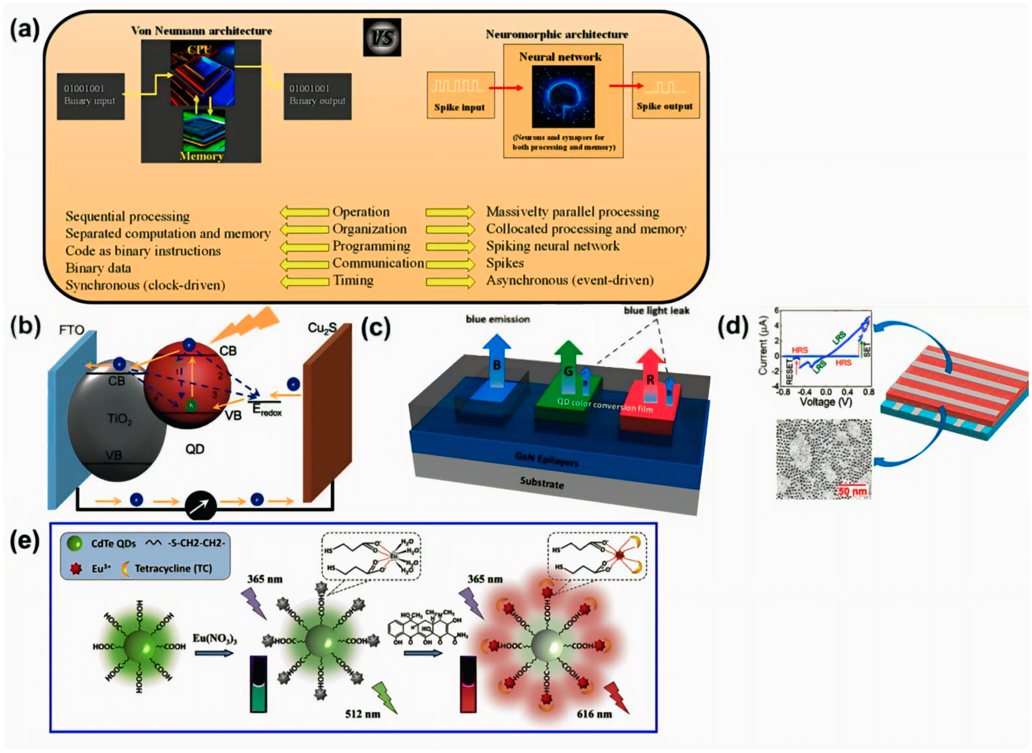
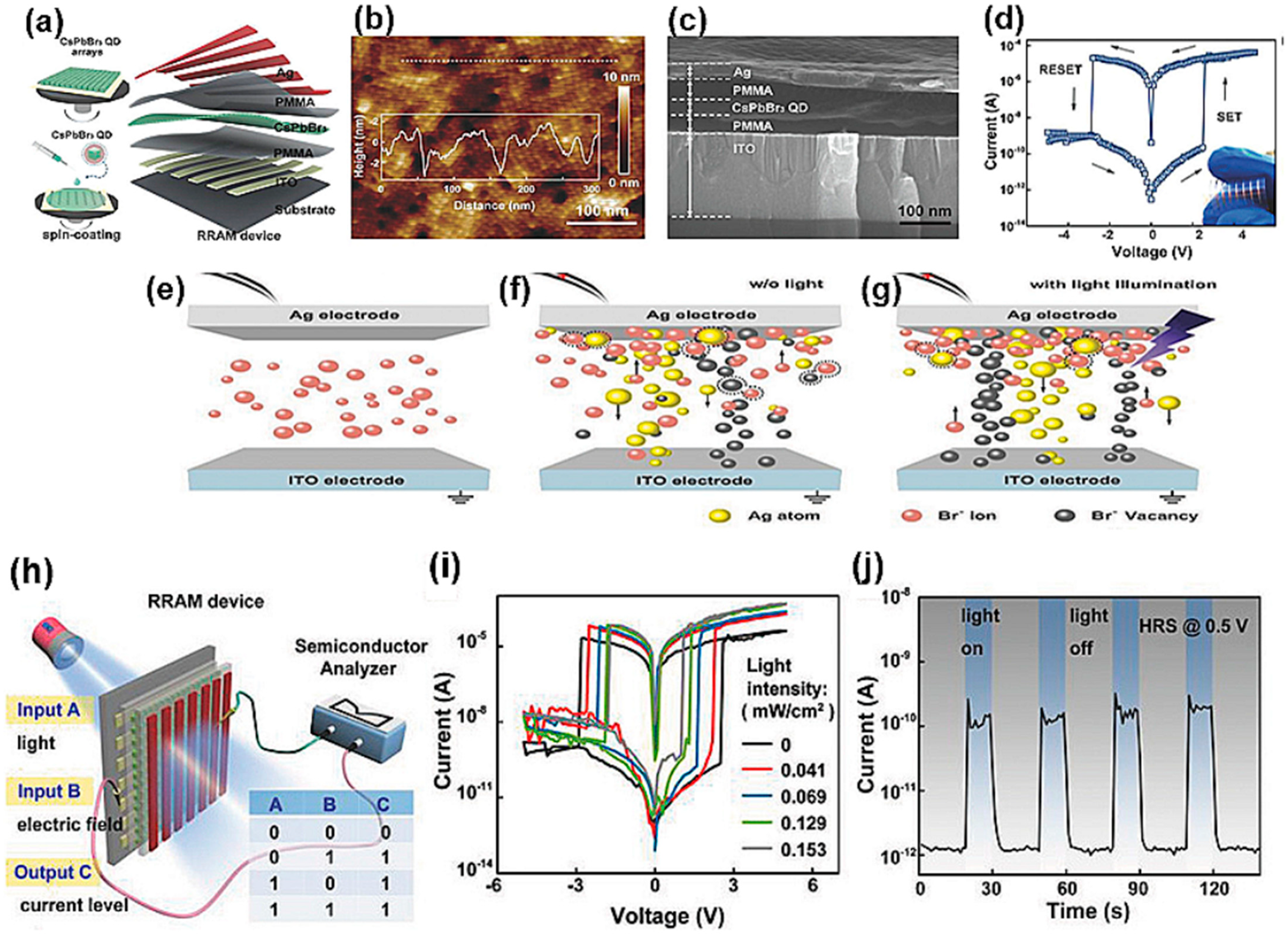
:1. Introduction
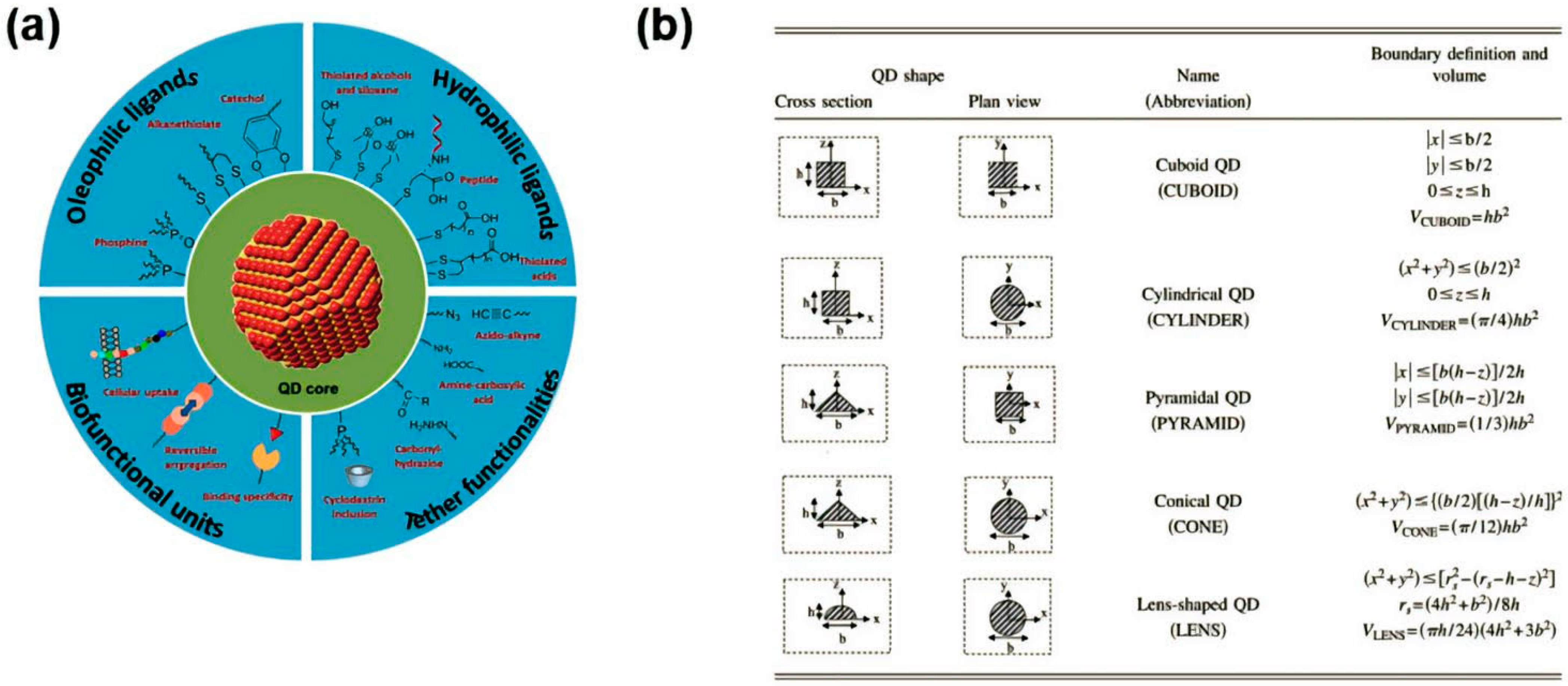
2. Quantum Dots
2.1. Material Properties of QDs
2.2. QD Manufacturing
2.2.1. Recent Quantum Dot Synthesis Techniques
2.2.2. Synthesis Methods for QDs
2.2.3. Size
3. Resistive Random Access Memory
3.1. RRAM Mechanism
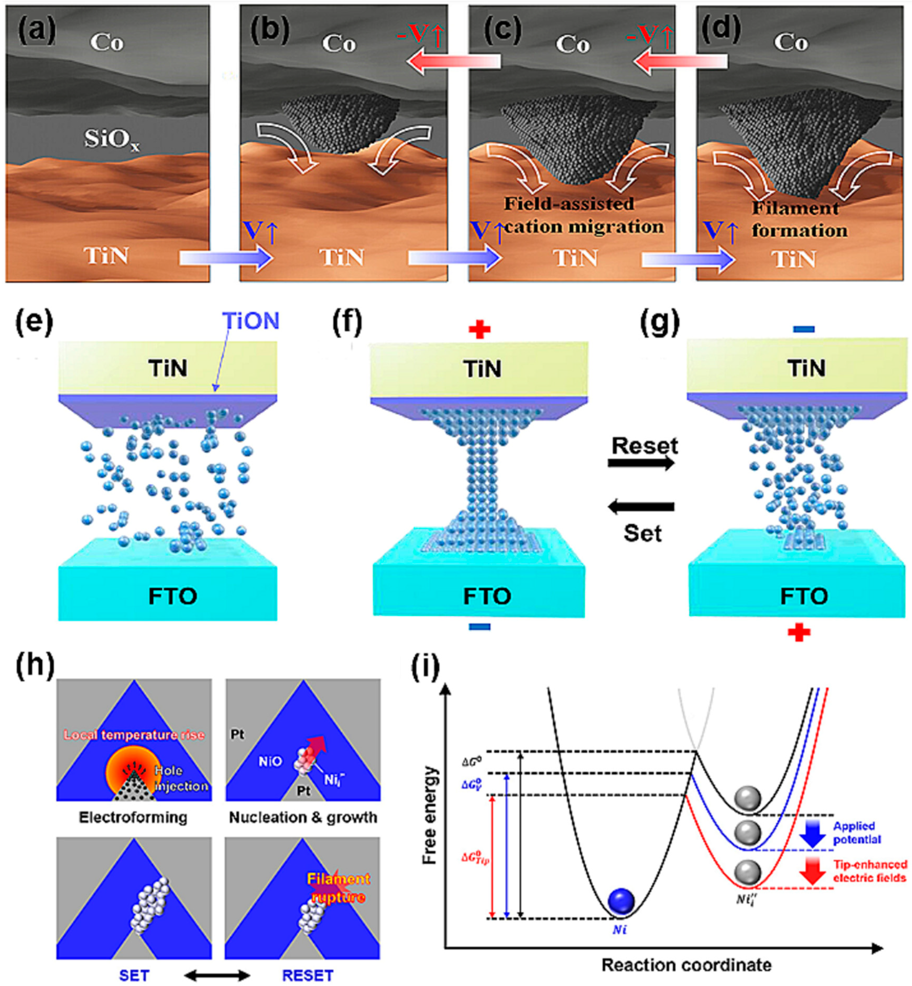
3.1.1. ECM
3.1.2. VCM
3.1.3. Thermochemical Mechanism
3.2. RRAM Materials
3.2.1. Inorganic

| Device Structure | VSET (V) | VRESET (V) | On/Off Ratio | Endurance | Retention | Synaptic Simulation | Reference |
|---|---|---|---|---|---|---|---|
| Ag/VOX/Pt | 0.23 | −0.07 | 103 | 103 | 12 h | - | [102] |
| Ti/ZrOX/HfOX/TiN | −2.0 | 2.4 | 103 | 3 × 10² | 104 | Potentiation /Depression (P/D) | [103] |
| TiN/HfOX/HfOY/HfOX/TiN | 0.27 | −0.25 | - | 2 × 10³ | 104 | [104] | |
| Ti/TaOX/indium tin oxide (ITO) | 2.1 | −2.1 | 102 | 103 | 104 | P/D, STDP, MNIST | [105] |
| Ag/TiOXNY/Ga2O3/Pt | 0.17 | −0.057 | 105 | 50 | 104 | [106] | |
| Ti/NiFe2O4/Pt | 0.75 | −0.06 | 102 | 102 | EPSC | [107] | |
| Pt/HfOX/AlOX/TiN | 2.2 | −2.0 | 103 | 104 | 104 | STDP, SRDP, EPSC, PPF | [108] |
| Ta/SiNX/Pt | 1.3 | −1.1 | 103 | 5 × 10² | 3 × 10² | [109] | |
| W/SiNX/n-Si | 4.0 | −4.0 | 103 | 8 × 10³ | MNIST (93.34%) | [110] | |
| Ti/HfOX/Pt | 0.5 | −0.5 | 102 | 104 | 106 | [111] |

3.2.2. Organic
3.2.3. Low-Dimensional Materials
4. QD-Based RRAM
5. Application
5.1. Artificial Synapses
5.2. Other Applications
6. Conclusions
Author Contributions
Funding
Conflicts of Interest
References
- Ahn, J.H.; Choi, H.S.; Kim, J.N.; Park, B.G.; Kim, S.; Lee, J.; Kim, Y. On-Chip Adaptive Matching Learning with Charge-Trap Synapse Device and ReLU Activation Circuit. Solid State Electron. 2021, 186, 108177. [Google Scholar] [CrossRef]
- Zahoor, F.; Azni Zulkifli, T.Z.; Khanday, F.A. Resistive Random Access Memory (RRAM): An Overview of Materials, Switching Mechanism, Performance, Multilevel Cell (MLC) Storage, Modeling, and Applications. Nanoscale Res. Lett. 2020, 15, 90. [Google Scholar] [CrossRef] [PubMed]
- Perea, G.; Navarrete, M.; Araque, A. Tripartite Synapses: Astrocytes Process and Control Synaptic Information. Trends Neurosci. 2009, 32, 421–431. [Google Scholar] [CrossRef] [PubMed]
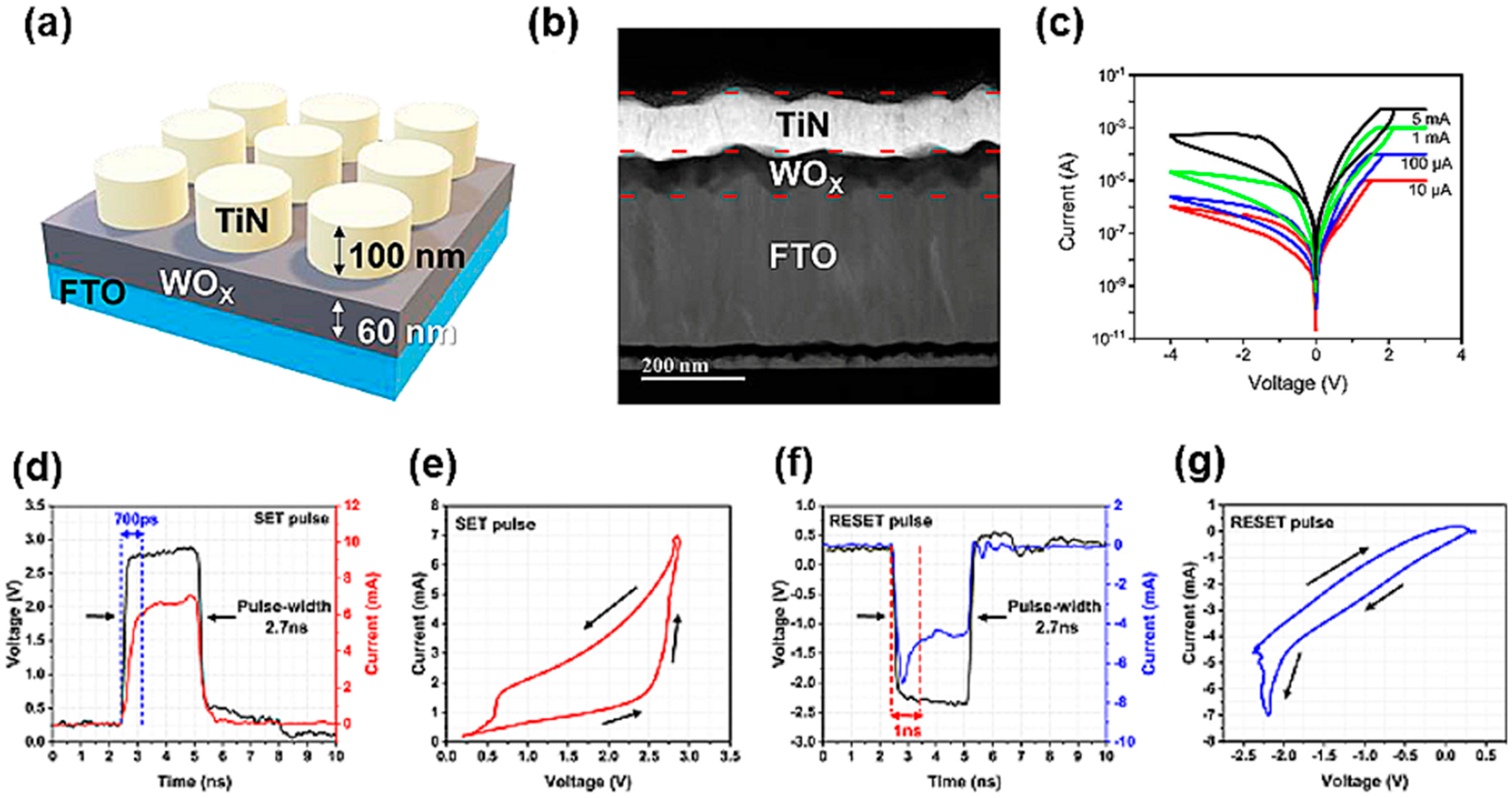
- Kim, G.; Cho, Y.; Kim, S. Short-Term Memory Characteristics of TiN/WOX/FTO-Based Transparent Memory Device. Chin. J. Phys. 2024, 88, 1044–1052. [Google Scholar] [CrossRef]
- Sawa, A. Resistive Switching in Transition Metal Oxides. Mater. Today 2008, 11, 28–36. [Google Scholar] [CrossRef]
- Li, Y.; Long, S.; Liu, Q.; Lv, H.; Liu, M. Resistive Switching Performance Improvement via Modulating Nanoscale Conductive Filament, Involving the Application of Two-Dimensional Layered Materials. Small 2017, 13, 1604306. [Google Scholar] [CrossRef]
- Shen, Z.; Zhao, C.; Qi, Y.; Xu, W.; Liu, Y.; Mitrovic, I.Z.; Yang, L.; Zhao, C. Advances of RRAM Devices: Resistive Switching Mechanisms, Materials and Bionic Synaptic Application. Nanomaterials 2020, 10, 1437. [Google Scholar] [CrossRef] [PubMed]
- Lv, Z.; Wang, Y.; Chen, J.; Wang, J.; Zhou, Y.; Han, S.T. Semiconductor Quantum Dots for Memories and Neuromorphic Computing Systems. Chem. Rev. 2020, 120, 3941–4006. [Google Scholar] [CrossRef]
- Rasal, A.S.; Yadav, S.; Kashale, A.A.; Altaee, A.; Chang, J.Y. Stability of Quantum Dot-Sensitized Solar Cells: A Review and Prospects. Nano Energy 2022, 94, 106854. [Google Scholar] [CrossRef]
- Dai, X.; Zhang, Z.; Jin, Y.; Niu, Y.; Cao, H.; Liang, X.; Chen, L.; Wang, J.; Peng, X. Solution-Processed, High-Performance Light-Emitting Diodes Based on Quantum Dots. Nature 2014, 515, 96–99. [Google Scholar] [CrossRef]
- Tang, J.; Wang, X.; Brzozowski, L.; Barkhouse, D.A.R.; Debnath, R.; Levina, L.; Sargent, E.H. Schottky Quantum Dot Solar Cells Stable in Air under Solar Illumination. Adv. Mater. 2010, 22, 1398–1402. [Google Scholar] [CrossRef] [PubMed]
- Martín-García, B.; Spirito, D.; Krahne, R.; Moreels, I. Solution-Processed Silver Sulphide Nanocrystal Film for Resistive Switching Memories. J. Mater. Chem. C Mater. 2018, 6, 13128–13135. [Google Scholar] [CrossRef]
- Li, X.; Rui, M.; Song, J.; Shen, Z.; Zeng, H. Carbon and Graphene Quantum Dots for Optoelectronic and Energy Devices: A Review. Adv. Funct. Mater. 2015, 25, 4929–4947. [Google Scholar] [CrossRef]
- Younis, A.; Chu, D.; Lin, X.; Yi, J.; Dang, F.; Li, S. High-Performance Nanocomposite Based Memristor with Controlled Quantum Dots as Charge Traps. American Chemical Society. Appl. Mater. Interfaces 2013, 5, 2249–2254. [Google Scholar] [CrossRef] [PubMed]
- Xu, Z.; Li, F.; Wu, C.; Ma, F.; Zheng, Y.; Yang, K.; Chen, W.; Hu, H.; Guo, T.; Kim, T.W. Ultrathin Electronic Synapse Having High Temporal/Spatial Uniformity and an Al2O3/Graphene Quantum Dots/Al2O3 Sandwich Structure for Neuromorphic Computing. NPG Asia Mater. 2019, 11, 18. [Google Scholar] [CrossRef]
- Lv, Z.; Wang, Y.; Chen, Z.; Sun, L.; Wang, J.; Chen, M.; Xu, Z.; Liao, Q.; Zhou, L.; Chen, X.; et al. Phototunable Biomemory Based on Light-Mediated Charge Trap. Adv. Sci. 2018, 5, 1800714. [Google Scholar] [CrossRef]
- Zhu, X.; Lu, W.D. Optogenetics-Inspired Tunable Synaptic Functions in Memristors. Am. Chem. Soc. Nano 2018, 12, 1242–1249. [Google Scholar] [CrossRef]
- Kumar, M.; Abbas, S.; Kim, J. All-Oxide-Based Highly Transparent Photonic Synapse for Neuromorphic Computing. Am. Chem. Soc. Appl. Mater. Interfaces 2018, 10, 34370–34376. [Google Scholar] [CrossRef]
- Baek, G.W.; Kim, Y.J.; Kim, J.; Chang, J.H.; Kim, U.; An, S.; Park, J.; Yu, S.; Bae, W.K.; Lim, J.; et al. Memristive Switching Mechanism in Colloidal InP/ZnSe/ZnS Quantum Dot-Based Synaptic Devices for Neuromorphic Computing. Nano Lett. 2024, 24, 5855–5861. [Google Scholar] [CrossRef]
- Betal, A.; Sahu, S. Study of Organic and Quantum Dots-Based Resistive Memory and Synaptic Devices. Ph.D. Thesis, Indian Institute of Technology Jodhpur, Jheepasani, India, 2023. [Google Scholar]
- Lin, C.Y.; Chen, J.; Chen, P.H.; Chang, T.C.; Wu, Y.; Eshraghian, J.K.; Moon, J.; Yoo, S.; Wang, Y.H.; Chen, W.C.; et al. Adaptive Synaptic Memory via Lithium Ion Modulation in RRAM Devices. Small 2020, 16, e2003964. [Google Scholar] [CrossRef]
- Caporale, N.; Dan, Y. Spike Timing-Dependent Plasticity: A Hebbian Learning Rule. Annu. Rev. Neurosci. 2008, 31, 25–46. [Google Scholar] [CrossRef] [PubMed]
- Kheradpisheh, S.R.; Ganjtabesh, M.; Thorpe, S.J.; Masquelier, T. STDP-Based Spiking Deep Convolutional Neural Networksa for Object Recognition. Neural Netw. 2018, 99, 56–67. [Google Scholar] [CrossRef] [PubMed]
- Yan, X.; Pei, Y.; Chen, H.; Zhao, J.; Zhou, Z.; Wang, H.; Zhang, L.; Wang, J.; Li, X.; Qin, C.; et al. Self-Assembled Networked PbS Distribution Quantum Dots for Resistive Switching and Artificial Synapse Performance Boost of Memristors. Adv. Mater. 2019, 31, e1805284. [Google Scholar] [CrossRef] [PubMed]
- Kutluyarov, R.V.; Zakoyan, A.G.; Voronkov, G.S.; Grakhova, E.P.; Butt, M.A. Neuromorphic Photonics Circuits: Contemporary Review. Nanomaterials 2023, 13, 3139. [Google Scholar] [CrossRef]
- Selopal, G.S.; Zhao, H.; Wang, Z.M.; Rosei, F. Core/Shell Quantum Dots Solar Cells. Adv. Funct. Mater. 2020, 30, 1908762. [Google Scholar] [CrossRef]
- Hyun, B.R.; Sher, C.W.; Chang, Y.W.; Lin, Y.; Liu, Z.; Kuo, H.C. Dual Role of Quantum Dots as Color Conversion Layer and Suppression of Input Light for Full-Color Micro-LED Displays. J. Phys. Chem. Lett. 2021, 12, 6946–6954. [Google Scholar] [CrossRef]
- Bera, J.; Betal, A.; Sharma, A.; Shankar, U.; Rath, A.K.; Sahu, S. CdSe Quantum Dot-Based Nanocomposites for Ultralow-Power Memristors. ACS Appl. Nano Mater. 2022, 5, 8502–8510. [Google Scholar] [CrossRef]
- Han, S.; Yang, L.; Wen, Z.; Chu, S.; Wang, M.; Wang, Z.; Jiang, C. A Dual-Response Ratiometric Fluorescent Sensor by Europium-Doped CdTe Quantum Dots for Visual and Colorimetric Detection of Tetracycline. J. Hazard. Mater. 2020, 398, e122894. [Google Scholar] [CrossRef]
- Chen, X.; Shehzad, K.; Gao, L.; Long, M.; Guo, H.; Qin, S.; Wang, X.; Wang, F.; Shi, Y.; Hu, W.; et al. Graphene Hybrid Structures for Integrated and Flexible Optoelectronics. Adv. Mater. 2020, 32, e1902039. [Google Scholar] [CrossRef]
- Wang, L.J.; Cao, G.; Tu, T.; Li, H.O.; Zhou, C.; Hao, X.J.; Su, Z.; Guo, G.C.; Jiang, H.W.; Guo, G.P. A Graphene Quantum Dot with a Single Electron Transistor as an Integrated Charge Sensor. Appl. Phys. Lett. 2010, 97, 262113. [Google Scholar] [CrossRef]
- Ji, Y.; Lee, S.A.; Cha, A.N.; Goh, M.; Bae, S.; Lee, S.; Son, D.I.; Kim, T.W. Resistive Switching Characteristics of ZnO-Graphene Quantum Dots and Their Use as an Active Component of an Organic Memory Cell with One Diode-One Resistor Architecture. Org. Electron. 2015, 18, 77–83. [Google Scholar] [CrossRef]
- Mansur, A.A.P.; Mansur, H.S.; Ramanery, F.P.; Oliveira, L.C.; Souza, P.P. “Green” Colloidal ZnS Quantum Dots/Chitosan Nano-Photocatalysts for Advanced Oxidation Processes: Study of the Photodegradation of Organic Dye Pollutants. Appl. Catal. B 2014, 158–159, 269–279. [Google Scholar] [CrossRef]
- Bao, J.; Bawendi, M.G. A Colloidal Quantum Dot Spectrometer. Nature 2015, 523, 67–70. [Google Scholar] [CrossRef] [PubMed]
- Yang, C.M.; Chen, T.C.; Verma, D.; Li, L.J.; Liu, B.; Chang, W.H.; Lai, C.S. Bidirectional All-Optical Synapses Based on a 2D Bi2O2Se/Graphene Hybrid Structure for Multifunctional Optoelectronics. Adv. Funct. Mater. 2020, 30, 2001598. [Google Scholar] [CrossRef]
- Bajorowicz, B.; Kobylański, M.P.; Gołąbiewska, A.; Nadolna, J.; Zaleska-Medynska, A.; Malankowska, A. Quantum Dot-Decorated Semiconductor Micro- and Nanoparticles: A Review of Their Synthesis, Characterization and Application in Photocatalysis. Adv. Colloid Interface Sci. 2018, 256, 352–372. [Google Scholar] [CrossRef] [PubMed]
- Bawendi, M.G.; Steigerwald, M.L.; Brus, L.E. The Quantum Mechanics of Larger Semiconductor Clusters (“Quantum Dots”). Annu. Rev. Phys. Chem 1990, 41, 477–496. [Google Scholar] [CrossRef]
- Moon, H.; Lee, C.; Lee, W.; Kim, J.; Chae, H. Stability of Quantum Dots, Quantum Dot Films, and Quantum Dot Light-Emitting Diodes for Display Applications. Adv. Mater. 2019, 31, e1804294. [Google Scholar] [CrossRef]
- Aroutiounian, V.; Petrosyan, S.; Khachatryan, A.; Touryan, K. Quantum Dot Solar Cells. J. Appl. Phys. 2001, 89, 2268–2271. [Google Scholar] [CrossRef]
- Xu, Q.; Niu, Y.; Li, J.; Yang, Z.; Gao, J.; Ding, L.; Ni, H.; Zhu, P.; Liu, Y.; Tang, Y.; et al. Recent Progress of Quantum Dots for Energy Storage Applications. Carbon. Neutrality 2022, 1, 13. [Google Scholar] [CrossRef]
- Hu, L.; Zhao, Q.; Huang, S.; Zheng, J.; Guan, X.; Patterson, R.; Kim, J.; Shi, L.; Lin, C.H.; Lei, Q.; et al. Flexible and Efficient Perovskite Quantum Dot Solar Cells via Hybrid Interfacial Architecture. Nat. Commun. 2021, 12, 466. [Google Scholar] [CrossRef]
- Weigert, F.; Müller, A.; Häusler, I.; Geißler, D.; Skroblin, D.; Krumrey, M.; Unger, W.; Radnik, J.; Resch-Genger, U. Combining HR-TEM and XPS to Elucidate the Core–Shell Structure of Ultrabright CdSe/CdS Semiconductor Quantum Dots. Sci. Rep. 2020, 10, 20712. [Google Scholar] [CrossRef] [PubMed]
- Chen, W.; Shen, J.; Lv, G.; Li, D.; Hu, Y.; Zhou, C.; Liu, X.; Dai, Z. Green Synthesis of Graphene Quantum Dots from Cotton Cellulose. ChemistrySelect 2019, 4, 2898–2902. [Google Scholar] [CrossRef]
- Van Avermaet, H.; Schiettecatte, P.; Hinz, S.; Giordano, L.; Ferrari, F.; Nayral, C.; Delpech, F.; Maultzsch, J.; Lange, H.; Hens, Z. Full-Spectrum InP-Based Quantum Dots with Near-Unity Photoluminescence Quantum Efficiency. ACS Nano 2022, 16, 9701–9712. [Google Scholar] [CrossRef] [PubMed]
- Korala, L.; Wang, Z.; Liu, Y.; Maldonado, S.; Brock, S.L. Uniform Thin Films of CdSe and CdSe(ZnS) Core(Shell) Quantum Dots by Sol-Gel Assembly: Enabling Photoelectrochemical Characterization and Electronic Applications. ACS Nano 2013, 7, 1215–1223. [Google Scholar] [CrossRef] [PubMed]
- Pu, Y.; Cai, F.; Wang, D.; Wang, J.X.; Chen, J.F. Colloidal Synthesis of Semiconductor Quantum Dots toward Large-Scale Production: A Review. Ind. Eng. Chem. Res. 2018, 57, 1790–1802. [Google Scholar] [CrossRef]
- Mashford, B.; Baldauf, J.; Nguyen, T.L.; Funston, A.M.; Mulvaney, P. Synthesis of Quantum Dot Doped Chalcogenide Glasses via Sol-Gel Processing. J. Appl. Phys. 2011, 109, 094305. [Google Scholar] [CrossRef]
- Devi, M.; Rawat, S. A Comprehensive Review of the Pyrolysis Process: From Carbon Nanomaterial Synthesis to Waste Treatment. Oxf. Open Mater. Sci. 2021, 1, itab014. [Google Scholar] [CrossRef]
- LiMoSani, F.; Carcione, R.; Antolini, F. Formation of CdSe Quantum Dots from Single Source Precursor Obtained by Thermal and Laser Treatment. J. Vac. Sci. Technol. B Nanotechnol. Microelectron. Mater. Process. Meas. Phenom. 2020, 38, 012802. [Google Scholar] [CrossRef]
- Bhattacharjee, A.; Ahmaruzzaman, M. Photocatalytic-Degradation and Reduction of Organic Compounds Using SnO2 Quantum Dots (via a Green Route) under Direct Sunlight. RSC Adv. 2015, 5, 66122–66133. [Google Scholar] [CrossRef]
- Prudhvi Raju, N.; Tripathi, D.; Lahiri, S.; Thangavel, R. Heat Reflux Sonochemical Synthesis of Cu3BiS3 Quantum Dots: Experimental and First-Principles Investigation of Spin–Orbit Coupling on Structural, Electronic, and Optical Properties. Sol. Energy 2023, 259, 107–118. [Google Scholar] [CrossRef]
- Gurel, A.; Avignon, F.; Wang, G.; Lau, S.; Piquemal, J.Y.; Perruchot, C.; Schaming, D. Electrochemical Synthesis of Nitrogen-Doped Graphene Quantum Dots and Their Photocatalytic Hydrogen Evolution Application. Carbon. Trends 2024, 15, 100354. [Google Scholar] [CrossRef]
- Schwan, J. Non-Thermal Plasmas and Material Synthesis: Applications in Quantum Dots, Lithium-Ion Batteries, and Pathogen Decontamination. Ph.D. Thesis, University of California Riverside, Riverside, CA, USA, 2023. [Google Scholar]
- Ondry, J.C.; Philbin, J.P.; Lostica, M.; Rabani, E.; Alivisatos, A.P. Colloidal Synthesis Path to 2D Crystalline Quantum Dot Superlattices. ACS Nano 2021, 15, 2251–2262. [Google Scholar] [CrossRef] [PubMed]
- Lang, J.; Li, X.; Yang, J.; Yang, L.; Zhang, Y.; Yan, Y.; Han, Q.; Wei, M.; Gao, M.; Liu, X.; et al. Rapid Synthesis and Luminescence of the Eu3+, Er3+ Codoped ZnO Quantum-Dot Chain via Chemical Precipitation Method. Appl. Surf. Sci. 2011, 257, 9574–9577. [Google Scholar] [CrossRef]
- Arachchige, I.U.; Brock, S.L. Sol-Gel Methods for the Assembly of Metal Chalcogenide Quantum Dots. Acc. Chem. Res. 2007, 40, 801–809. [Google Scholar] [CrossRef] [PubMed]
- Xue, L.; Shen, C.; Zheng, M.; Lu, H.; Li, N.; Ji, G.; Pan, L.; Cao, J. Hydrothermal Synthesis of Graphene-ZnS Quantum Dot Nanocomposites. Mater. Lett. 2011, 65, 198–200. [Google Scholar] [CrossRef]
- Ramanery, F.P.; Mansur, A.A.; Mansur, H.S. One-Step Colloidal Synthesis of Biocompatible Water-Soluble ZnS Quantum Dot/Chitosan Nanoconjugates. Nanoscale Res. Lett. 2013, 8, 512. [Google Scholar] [CrossRef]
- Wood, V.; Bulović, V. Colloidal Quantum Dot Light-Emitting Devices. Nano Rev. 2010, 1, 5202. [Google Scholar] [CrossRef]
- Čapek, R.K.; Yanover, D.; Lifshitz, E. Size Control by Rate Control in Colloidal PbSe Quantum Dot Synthesis. Nanoscale 2015, 7, 5299–5310. [Google Scholar] [CrossRef]
- Lutz, T.; MacLachlan, A.; Sudlow, A.; Nelson, J.; Hill, M.S.; Molloy, K.C.; Haque, S.A. Thermal Decomposition of Solution Processable Metal Xanthates on Mesoporous Titanium Dioxide Films: A New Route to Quantum-Dot Sensitised Heterojunctions. Phys. Chem. Chem. Phys. 2012, 14, 16192–16196. [Google Scholar] [CrossRef]
- Zhang, J.; Li, S.; Xiong, H.; Tian, W.; Li, Y.; Fang, Y.; Wu, Z.; Dai, J.; Xu, J.; Li, X.; et al. Fabrication of Low-Density GaN/AlN Quantum Dots via GaN Thermal Decomposition in MOCVD. Nanoscale Res. Lett. 2014, 9, 1–5. [Google Scholar] [CrossRef]
- Tilley, R.D.; Yamamoto, K. The Microemulsion Synthesis of Hydrophobic and Hydrophilic Silicon Nanocrystals. Adv. Mater. 2006, 18, 2053–2056. [Google Scholar] [CrossRef]
- Zhang, Y.; Shi, C.; Dai, X.; Liu, F.; Fang, X.; Zhu, J. Pyrolysis Preparation of Cu2ZnSnS4 Thin Film and Its Application to Counter Electrode in Quantum Dot-Sensitized Solar Cells. Electrochim. Acta 2014, 118, 41–44. [Google Scholar] [CrossRef]
- Wang, L.; Rastelli, A.; Kiravittaya, S.; Benyoucef, M.; Schmidt, O.G. Self-Assembled Quantum Dot Molecules. Adv. Mater. 2009, 21, 2601–2618. [Google Scholar] [CrossRef] [PubMed]
- Liang, Y.C.; Liu, K.K.; Lu, Y.J.; Zhao, Q.; Shan, C.X. Silica Encapsulated ZnO Quantum Dot-Phosphor Nanocomposites: Sol-Gel Preparation and White Light-Emitting Device Application. Chin. Phys. B 2018, 27, 078102. [Google Scholar] [CrossRef]
- Martucci, A.; Fick, J.; LeBlanc, S.É.; LoCascio, M.; Haché, A. Optical Properties of PbS Quantum Dot Doped Sol-Gel Films. J. Non-Cryst. Solids 2004, 345–346, 639–642. [Google Scholar] [CrossRef]
- Chrzanowski, M.; Kuchowicz, M.; Szukiewicz, R.; Sitarek, P.; Misiewicz, J.; Podhorodecki, A. Enhanced Efficiency of Quantum Dot Light-Emitting Diode by Sol-Gel Derived Zn1-xMgxO Electron Transport Layer. Org. Electron. 2020, 80, 105656. [Google Scholar] [CrossRef]
- Yang, J.; Choi, M.K.; Kim, D.H.; Hyeon, T. Designed Assembly and Integration of Colloidal Nanocrystals for Device Applications. Adv. Mater. 2016, 28, 1176–1207. [Google Scholar] [CrossRef]
- Lachance-Quirion, D.; Tremblay, S.; Lamarre, S.A.; Méthot, V.; Gingras, D.; Camirand Lemyre, J.; Pioro-Ladrière, M.; Allen, C.N. Telegraphic Noise in Transport through Colloidal Quantum Dots. Nano Lett. 2014, 14, 882–887. [Google Scholar] [CrossRef]
- Liu, Y.; Tolentino, J.; Gibbs, M.; Ihly, R.; Perkins, C.L.; Liu, Y.; Crawford, N.; Hemminger, J.C.; Law, M. PbSe Quantum Dot Field-Effect Transistors with Air-Stable Electron Mobilities above 7 cm2 V−1 s−1. Nano Lett. 2013, 13, 1578–1587. [Google Scholar] [CrossRef]
- Zhang, H.; Kurley, J.M.; Russell, J.C.; Jang, J.; Talapin, D.V. Solution-Processed, Ultrathin Solar Cells from CdCl3−-Capped CdTe Nanocrystals: The Multiple Roles of CdCl3− Ligands. J. Am. Chem. Soc. 2016, 138, 7464–7467. [Google Scholar] [CrossRef]
- Wills, A.W.; Kang, M.S.; Khare, A.; Gladfelter, W.L.; Norris, D.J. Thermally Degradable Ligands for Nanocrystals. ACS Nano 2010, 4, 4523–4530. [Google Scholar] [CrossRef] [PubMed]
- Dong, X.; Wang, K.; Bu, Y.; Wang, X. Ligand Modification Enhanced Quantum Dot LEDs: Principles and Methods. J. Mater. Chem. C Mater. 2023, 11, 11755–11775. [Google Scholar] [CrossRef]
- Zhou, J.; Liu, Y.; Tang, J.; Tang, W. Surface Ligands Engineering of Semiconductor Quantum Dots for CheMoSensory and Biological Applications. Mater. Today 2017, 20, 360–376. [Google Scholar] [CrossRef]
- Ngo, C.Y.; Yoon, S.F.; Fan, W.J.; Chua, S.J. Effects of Size and Shape on Electronic States of Quantum Dots. Phys. Rev. B Condens. Matter Mater. Phys. 2006, 74. [Google Scholar] [CrossRef]
- Russo, U.; Ielmini, D.; Cagli, C.; Lacaita, A.L. Filament Conduction and Reset Mechanism in NiO-Based Resistive-Switching Memory (RRAM) Devices. IEEE Trans. Electron Devices 2009, 56, 186–192. [Google Scholar] [CrossRef]
- Hu, R.; Li, X.; Tang, J.; Li, Y.; Zheng, X.; Gao, B.; Qian, H.; Wu, H. Investigation of Resistive Switching Mechanisms in Ti/TiOx/Pd-Based RRAM Devices. Adv. Electron. Mater. 2022, 8, 2100827. [Google Scholar] [CrossRef]
- Lee, J.S.; Lee, S.; Noh, T.W. Resistive Switching Phenomena: A Review of Statistical Physics Approaches. Appl. Phys. Rev. 2015, 2, 031303. [Google Scholar] [CrossRef]
- Milo, V.; Glukhov, A.; Perez, E.; Zambelli, C.; Lepri, N.; Mahadevaiah, M.K.; Quesada, E.P.B.; Olivo, P.; Wenger, C.; Ielmini, D. Accurate Program/Verify Schemes of Resistive Switching Memory (RRAM) for In-Memory Neural Network Circuits. IEEE Trans. Electron Devices 2021, 68, 3832–3837. [Google Scholar] [CrossRef]
- Qian, M.; Gao, H.; Duan, Y.; Guo, J.; Bai, Y.; Zhu, S.; Ma, X.; Yang, Y. Effect of the Bottom Electrode on the Digital and Analog Resistive Switching Behavior of SiNx-Based RRAM. Appl. Phys. Lett. 2023, 123, 033501. [Google Scholar] [CrossRef]
- Hu, L.; Gao, W.; Xiao, M.; Li, Z. Interfacial Reaction Induced Digital-to-Analog Resistive Switching in TiO2-Based Memory Devices. Phys. B Condens. Matter 2022, 632, 413730. [Google Scholar] [CrossRef]
- Park, H.; Ju, D.; Mahata, C.; Emelyanov, A.; Koo, M.; Kim, S. Long-and Short-Term Memory Characteristics Controlled by Electrical and Optical Stimulations in InZnO-Based Synaptic Device for Reservoir Computing. Adv. Electron. Mater. 2024, 10, 2300911. [Google Scholar] [CrossRef]
- Milozzi, A.; Ricci, S.; Ielmini, D. Memristive Tonotopic Mapping with Volatile Resistive Switching Memory Devices. Nat. Commun. 2024, 15, 2812. [Google Scholar] [CrossRef] [PubMed]
- Yang, S.J.; Liang, L.; Lee, Y.; Gu, Y.; Fatheema, J.; Kutagulla, S.; Kim, D.; Kim, M.; Kim, S.; Akinwande, D. Volatile and Nonvolatile Resistive Switching Coexistence in Conductive Point Hexagonal Boron Nitride Monolayer. ACS Nano 2024, 18, 3313–3322. [Google Scholar] [CrossRef] [PubMed]
- Shi, T.; Wang, R.; Wu, Z.; Sun, Y.; An, J.; Liu, Q. A Review of Resistive Switching Devices: Performance Improvement, Characterization, and Applications. Small Struct. 2021, 2, 2000109. [Google Scholar] [CrossRef]
- Yang, R. Review of Resistive Switching Mechanisms for Memristive Neuromorphic Devices. Chin. Phys. B 2020, 29, 097305. [Google Scholar] [CrossRef]
- Khan, R.; Ilyas, N.; Shamim, M.Z.M.; Khan, M.I.; Sohail, M.; Rahman, N.; Khan, A.A.; Khan, S.N.; Khan, A. Oxide-Based Resistive Switching-Based Devices: Fabrication, Influence Parameters and Applications. J. Mater. Chem. C Mater. 2021, 9, 15755–15788. [Google Scholar] [CrossRef]
- Teja Nibhanupudi, S.S.; Roy, A.; Veksler, D.; Coupin, M.; Matthews, K.C.; Disiena, M.; Ansh; Singh, J.V.; Gearba-Dolocan, I.R.; Warner, J.; et al. Ultra-Fast Switching Memristors Based on Two-Dimensional Materials. Nat. Commun. 2024, 15, 2334. [Google Scholar] [CrossRef]
- Vorontsov, V.A.; Antonov, D.A.; Kruglov, A.V.; Antonov, I.N.; Shenina, M.E.; Kotomina, V.E.; Shengurov, V.G.; Denisov, S.A.; Chalkov, V.Y.; Pavlov, D.A.; et al. Investigation of Resistive Switching in Ag/Ge/Si(001) Stack by Conductive Atomic Force Microscopy. J. Phys. Conf. Ser. 2021, 2086, 012043. [Google Scholar] [CrossRef]
- Yong, Z.; Persson, K.M.; Saketh Ram, M.; D’Acunto, G.; Liu, Y.; Benter, S.; Pan, J.; Li, Z.; Borg, M.; Mikkelsen, A.; et al. Tuning Oxygen Vacancies and Resistive Switching Properties in Ultra-Thin HfO2 RRAM via TiN Bottom Electrode and Interface Engineering. Appl. Surf. Sci. 2021, 551, 149386. [Google Scholar] [CrossRef]
- Russo, U.; Jelmini, D.; Cagli, C.; Lacaita, A.L.; Spigat, S.; Wiemert, C.; Peregot, M.; Fanciullit, M. Conductive-Filament Switching Analysis and Self-Accelerated Thermal Dissolution Model for Reset in NiO-Based RRAM. In Proceedings of the 2007 IEEE International Electron Devices Meeting, Washington, DC, USA, 10–12 December 2007; IEEE: Piscataway, NJ, USA, 2007. [Google Scholar]
- Kim, T.; Vogel, T.; Piros, E.; Nasiou, D.; Kaiser, N.; Schreyer, P.; Winkler, R.; Zintler, A.; Arzumanov, A.; Petzold, S.; et al. Oxide Thickness-Dependent Resistive Switching Characteristics of Cu/HfO2/Pt ECM Devices. Appl. Phys. Lett. 2023, 122, 023502. [Google Scholar] [CrossRef]
- Shi, Y.; Oh, S.; Park, J.; del Valle, J.; Salev, P.; Schuller, I.K.; Kuzum, D. Integration of Ag-CBRAM Crossbars and Mott ReLU Neurons for Efficient Implementation of Deep Neural Networks in Hardware. Neuromorphic Comput. Eng. 2023, 3, 034007. [Google Scholar] [CrossRef]
- Choi, Y.J.; Bang, S.; Kim, T.H.; Hong, K.; Kim, S.; Kim, S.; Park, B.G.; Choi, W.Y. Electric-Field-Induced Metal Filament Formation in Cobalt-Based CBRAM Observed by TEM. ACS Appl. Electron. Mater. 2023, 5, 1834–1843. [Google Scholar] [CrossRef]
- Choi, H.H.; Paik, S.H.; Kim, Y.; Kim, M.; Kang, Y.S.; Lee, S.S.; Jho, J.Y.; Park, J.H. Facilitation of the Thermochemical Mechanism in NiO-Based Resistive Switching Memories via Tip-Enhanced Electric Fields. J. Ind. Eng. Chem. 2021, 94, 233–239. [Google Scholar] [CrossRef]
- Joshua Yang, J.; Miao, F.; Pickett, M.D.; Ohlberg, D.A.A.; Stewart, D.R.; Lau, C.N.; Williams, R.S. The Mechanism of Electroforming of Metal Oxide Memristive Switches. Nanotechnology 2009, 20, 215201. [Google Scholar] [CrossRef] [PubMed]
- Wang, Y.; Liu, Q.; Long, S.; Wang, W.; Wang, Q.; Zhang, M.; Zhang, S.; Li, Y.; Zuo, Q.; Yang, J.; et al. Investigation of Resistive Switching in Cu-Doped HfO2 Thin Film for Multilevel Non-Volatile Memory Applications. Nanotechnology 2010, 21, 045202. [Google Scholar] [CrossRef] [PubMed]
- Guan, W.; Long, S.; Liu, Q.; Liu, M.; Wang, W. Nonpolar Nonvolatile Resistive Switching in Cu Doped ZrO2. IEEE Electron. Device Lett. 2008, 29, 434–437. [Google Scholar] [CrossRef]
- Ni, M.C.; Guo, S.M.; Tian, H.F.; Zhao, Y.G.; Li, J.Q. Resistive Switching Effect in SrTiO3-δ/Nb-Doped SrTiO3 Heterojunction. Appl. Phys. Lett. 2007, 91, 183502. [Google Scholar] [CrossRef]
- Li, S.L.; Gang, J.L.; Li, J.; Chu, H.F.; Zheng, D.N. Reproducible Low-Voltage Resistive Switching in a Low-Initial-Resistance Pr0.7Ca0.3MnO3 Junction. J. Phys. D Appl. Phys. 2008, 41, 185409. [Google Scholar] [CrossRef]
- Ryu, J.; Park, K.; Sahu, D.P.; Yoon, T.S. Forming-Free, Low-Voltage, and High-Speed Resistive Switching in Ag/Oxygen-Deficient Vanadium Oxide(VOx)/Pt Device through Two-Step Resistance Change by Ag Filament Formation. ACS Appl. Mater. Interfaces 2024, 16, 26450–26459. [Google Scholar] [CrossRef]
- Ji, H.; Lee, Y.; Heo, J.; Kim, S. Improved Resistive and Synaptic Switching Performances in Bilayer ZrOx/HfOx Devices. J. Alloys Compd. 2023, 962, 171096. [Google Scholar] [CrossRef]
- Yang, F.; Lou, S.; He, Z.; Liu, B.; Li, D.; Hu, B.; Wang, W. Optimization of the Forming Process of HfOx-Based RRAM to Achieve Bidirectional Forming and Enhanced Switching Performance by Inserting an Oxygen-Vacancy-Rich Layer. ACS Appl. Electron. Mater. 2024, 6, 3158–3166. [Google Scholar] [CrossRef]
- Ju, D.; Kim, J.H.; Kim, S. Highly Uniform Resistive Switching Characteristics of Ti/TaOx/ITO Memristor Devices for Neuromorphic System. J. Alloys Compd. 2023, 961, 170920. [Google Scholar] [CrossRef]
- Cui, D.; Lin, Z.; Kang, M.; Wang, Y.; Gao, X.; Su, J.; Miao, J.; Zhang, J.; Hao, Y.; Chang, J. High Performance Low Power Multilevel Oxide Based RRAM Devices Based on TiOxNy/Ga2O3 Hybrid Structure. Appl. Phys. Lett. 2024, 124, 122107. [Google Scholar] [CrossRef]
- Rajesh Kumar, R.; Kalaboukhov, A.; Weng, Y.C.; Rathod, K.N.; Johansson, T.; Lindblad, A.; Kamalakar, M.V.; Sarkar, T. Vacancy-Engineered Nickel Ferrite Forming-Free Low-Voltage Resistive Switches for Neuromorphic Circuits. ACS Appl. Mater. Interfaces 2024, 16, 19225–19234. [Google Scholar] [CrossRef]
- Kim, J.; Lee, S.; Kim, S.; Yang, S.; Lee, J.K.; Kim, T.H.; Ismail, M.; Mahata, C.; Kim, Y.; Choi, W.Y.; et al. Synaptic Characteristics and Vector-Matrix Multiplication Operation in Highly Uniform and Cost-Effective Four-Layer Vertical RRAM Array. Adv. Funct. Mater. 2024, 34, 2310193. [Google Scholar] [CrossRef]
- Gao, H.X.; Jiang, P.F.; Zhang, Z.F.; Yang, M.; Ma, X.H.; Yang, Y.T. Influence of Nitrogen Concentration on Self-Compliance Resistive Switching in Ta/SiNx/Pt RRAM Devices. Phys. Status Solidi (A) Appl. Mater. Sci. 2018, 215, 1800201. [Google Scholar] [CrossRef]
- Kim, C.S.; Kim, T.; Min, K.K.; Kim, Y.; Kim, S.; Park, B.G. Synaptic Device with High Rectification Ratio Resistive Switching and Its Impact on Spiking Neural Network. IEEE Trans. Electron Devices 2021, 68, 1610–1615. [Google Scholar] [CrossRef]
- Park, J.; Park, E.; Yu, H.Y. Active Layer Nitrogen Doping Technique with Excellent Thermal Stability for Resistive Switching Memristor. Appl. Surf. Sci. 2022, 603, 154307. [Google Scholar] [CrossRef]
- Han, S.W.; Park, C.J.; Shin, M.W. The Role of Al Atoms in Resistive Switching for Al/ZnO/Pt Resistive Random Access Memory (RRAM) Device. Surf. Interfaces 2022, 31, 102099. [Google Scholar] [CrossRef]
- Park, S.P.; Tak, Y.J.; Kim, H.J.; Lee, J.H.; Yoo, H.; Kim, H.J. Analysis of the Bipolar Resistive Switching Behavior of a Biocompatible Glucose Film for Resistive Random Access Memory. Adv. Mater. 2018, 30, e1800722. [Google Scholar] [CrossRef]
- Huang, Y.J.; Lee, S.C. Graphene/h-BN Heterostructures for Vertical Architecture of RRAM Design. Sci. Rep. 2017, 7, 9679. [Google Scholar] [CrossRef] [PubMed]
- Zheng, L.; Sun, B.; Chen, Y.; Li, T.; Mao, S.; Zhu, S.; Wang, H.; Zhang, Y.; Lei, M.; Zhao, Y. The Redox of Hydroxyl-Assisted Metallic Filament Induced Resistive Switching Memory Based on a Biomaterial-Constructed Sustainable and Environment-Friendly Device. Mater. Today Chem. 2018, 10, 167–174. [Google Scholar] [CrossRef]
- Cheong, K.Y.; Tayeb, I.A.; Zhao, F.; Abdullah, J.M. Review on Resistive Switching Mechanisms of Bio-Organic Thin Film for Non-Volatile Memory Application. Nanotechnol. Rev. 2021, 10, 680–709. [Google Scholar] [CrossRef]
- Liu, S.; Cheng, Y.; Han, F.; Fan, S.; Zhang, Y. Multilevel Resistive Switching Memristor Based on Silk Fibroin/Graphene Oxide with Image Reconstruction Functionality. Chem. Eng. J. 2023, 471, 144678. [Google Scholar] [CrossRef]
- Sahu, D.P.; Jammalamadaka, S.N. Detection of Bovine Serum Albumin Using Hybrid TiO2 + Graphene Oxide Based Bio–Resistive Random Access Memory Device. Sci. Rep. 2019, 9, 16141. [Google Scholar] [CrossRef] [PubMed]
- Khan, S.A.; Rahmani, M.K.; Kim, H.W.; Khan, M.F.; Yun, C.; Kang, M.H. Polymer-Based Non-Volatile Resistive Random-Access Memory Device Fabrication with Multi-Level Switching and Negative Differential Resistance State. Org. Electron. 2021, 96, 106228. [Google Scholar] [CrossRef]
- Ruan, W.; Hu, Y.; Xu, F.; Zhang, S. Resistive Switching Behavior of Organic-Metallic Halide Perovskites CH3NH3Pb1−xBixBr3. Org. Electron. 2019, 70, 252–257. [Google Scholar] [CrossRef]
- Shu, P.; Cao, X.; Du, Y.; Zhou, J.; Zhou, J.; Xu, S.; Liu, Y.; Cao, S. Resistive Switching Performance of Fibrous Crosspoint Memories Based on an Organic-Inorganic Halide Perovskite. J. Mater. Chem. C Mater. 2020, 8, 12865–12875. [Google Scholar] [CrossRef]
- Park, J.H.; Khan, S.A.; Rahmani, M.K.; Cho, J.; Kang, M.H. Enhancement of Resistive Switching Behavior of Organic Resistive Random Access Memory Devices through UV-Ozone Treatment. Mater. Res. Express 2022, 9, 085903. [Google Scholar] [CrossRef]
- Betal, A.; Bera, J.; Sahu, S. Non-Volatile Memristor-Based Artificial Synaptic Behavior of Redox-Active Organic Composites. J. Mater. Chem. C Mater. 2023, 11, 4674–4682. [Google Scholar] [CrossRef]
- Sun, Y.; Wen, D. Multistage Resistive Switching Behavior Organic Coating Films-Based of Memory Devices. Prog. Org. Coat. 2020, 142, 105613. [Google Scholar] [CrossRef]
- Jetty, P.; Jammalamadaka, S. Temperature Evolution of Charge Transport in Chitosan Based Bio-Resistive Random-Access Memory Device. Phys. Status Solidi (A) Appl. Mater. Sci. 2023, 220, 2300050. [Google Scholar] [CrossRef]
- Dwivedi, A.; Lodhi, A.; Saini, S.; Agarwal, H.; Tiwari, S.P. Fabrication and Modeling of Flexible High-Performance Resistive Switching Devices With Biomaterial Gelatin/Ultrathin HfOx Hybrid Bilayer. IEEE Trans. Electron Devices 2022, 69, 6423–6429. [Google Scholar] [CrossRef]
- Hussain, T.; Abbas, H.; Youn, C.; Lee, H.; Boynazarov, T.; Ku, B.; Jeon, Y.R.; Han, H.; Lee, J.H.; Choi, C.; et al. Cellulose Nanocrystal Based Bio-Memristor as a Green Artificial Synaptic Device for Neuromorphic Computing Applications. Adv. Mater. Technol. 2022, 7, 2100744. [Google Scholar] [CrossRef]
- Li, W.; Zhu, H.; Sun, T.; Qu, W.; Fan, X.; Gao, Z.; Shi, W.; Wei, B. High On/Off Ratio Organic Resistive Switching Memory Based on Carbazolyl Dicyanobenzene and a Polymer Composite. J. Phys. Chem. C 2022, 126, 12897–12905. [Google Scholar] [CrossRef]
- Patil, H.; Kim, H.; Rehman, S.; Kadam, K.D.; Aziz, J.; Khan, M.F.; Kim, D.K. Stable and Multilevel Data Storage Resistive Switching of Organic Bulk Heterojunction. Nanomaterials 2021, 11, 359. [Google Scholar] [CrossRef]
- Kim, T.; Kim, D.K.; Kim, J.; Pak, J.J. Resistive Switching Behaviour of Multi-Stacked PVA/Graphene Oxide + PVA Composite/PVA Insulating Layer-Based RRAM Devices. Semicond. Sci. Technol. 2019, 34, 065006. [Google Scholar] [CrossRef]
- Dai, Y.; Bao, W.; Hu, L.; Liu, C.; Yan, X.; Chen, L.; Sun, Q.; Ding, S.; Zhou, P.; Zhang, D.W. Forming Free and Ultralow-Power Erase Operation in Atomically Crystal TiO2 Resistive Switching. 2D Mater. 2017, 4, 025012. [Google Scholar] [CrossRef]
- Shan, L.; Wang, Z.; Wu, L.; Bao, S.; Chen, Y.S.; Tang, K.; Cai, Y.; Huang, R. Non-Linear Resistive Switching Characteristics in HFO2-Based RRAM with Low-Dimensional Material Engineered Interface. In Proceedings of the China Semiconductor Technology International Conference 2021, CSTIC 2021, Shanghai, China, 14–15 March 2021; Institute of Electrical and Electronics Engineers Inc.: Piscataway, NJ, USA, 2021. [Google Scholar]
- Sun, T.; Yu, F.; Tang, X.; Li, H.; Zhang, F.; Xu, Z.; Liao, Q.; Yu, Z.; Liu, X.; Wangyang, P.; et al. Organic-2D Composite Material-Based RRAM with High Reliability for Mimicking Synaptic Behavior. J. Mater. 2024, 10, 440–447. [Google Scholar] [CrossRef]
- Yan, X.; Zhang, L.; Yang, Y.; Zhou, Z.; Zhao, J.; Zhang, Y.; Liu, Q.; Chen, J. Highly Improved Performance in Zr0.5Hf0.5O2 Films Inserted with Graphene Oxide Quantum Dots Layer for Resistive Switching Non-Volatile Memory. J. Mater. Chem. C Mater. 2017, 5, 11046–11052. [Google Scholar] [CrossRef]
- El-Atab, N.; Cimen, F.; Alkis, S.; Okyay, A.K.; Nayfeh, A. Enhanced Memory Effect with Embedded Graphene Nanoplatelets in ZnO Charge Trapping Layer. Appl. Phys. Lett. 2014, 105, 033102. [Google Scholar] [CrossRef]
- Cosmin Obreja, A.; Cristea, D.; Mihalache, I.; Radoi, A.; Gavrila, R.; Comanescu, F.; Kusko, C. Charge Transport and Memristive Properties of Graphene Quantum Dots Embedded in Poly(3-Hexylthiophene) Matrix. Appl. Phys. Lett. 2014, 105, 083303. [Google Scholar] [CrossRef]
- Reshma, V.G.; Mohanan, P.V. Quantum Dots: Applications and Safety Consequences. J. Lumin. 2019, 205, 287–298. [Google Scholar] [CrossRef]
- Mahata, C.; Ju, D.; Das, T.; Jeon, B.; Ismail, M.; Kim, S.; Kim, S. Artificial Synapses Based on 2D-Layered Palladium Diselenide Heterostructure Dynamic Memristor for Neuromorphic Applications. Nano Energy 2024, 120, 109168. [Google Scholar] [CrossRef]
- Xia, Y.; Wang, J.; Chen, R.; Wang, H.; Xu, H.; Jiang, C.; Li, W.; Xiao, X. 2D Heterostructure of Bi2O2Se/Bi2SeOx Nanosheet for Resistive Random Access Memory. Adv. Electron. Mater. 2022, 8, 2200126. [Google Scholar] [CrossRef]
- Huang, Y.; Gu, Y.; Wu, X.; Ge, R.; Chang, Y.F.; Wang, X.; Zhang, J.; Akinwande, D.; Lee, J.C. ReSe2-Based RRAM and Circuit-Level Model for Neuromorphic Computing. Front. Nanotechnol. 2021, 3, 782836. [Google Scholar] [CrossRef]
- Casa Branca, N.; Deuermeier, J.; Martins, J.; Carlos, E.; Pereira, M.; Martins, R.; Fortunato, E.; Kiazadeh, A. 2D Resistive Switching Based on Amorphous Zinc–Tin Oxide Schottky Diodes. Adv. Electron. Mater. 2020, 6, 1900958. [Google Scholar] [CrossRef]
- Huang, C.H.; Chang, H.; Yang, T.Y.; Wang, Y.C.; Chueh, Y.L.; Nomura, K. Artificial Synapse Based on a 2D-SnO2 Memtransistor with Dynamically Tunable Analog Switching for Neuromorphic Computing. ACS Appl. Mater. Interfaces 2021, 13, 52822–52832. [Google Scholar] [CrossRef]
- Deshmukh, A.P.; Patil, K.; Ogale, S.; Bhave, T. Resistive Switching in CsPbBr3 (0D)/MoS2 (2D) Heterojunction System: Trap-Controlled Space Charge Limited Transport Mechanism. ACS Appl. Electron. Mater. 2023, 5, 1536–1545. [Google Scholar] [CrossRef]
- Tang, S.Y.; Shih, Y.C.; Shen, Y.C.; Cyu, R.H.; Chen, C.T.; Yang, T.Y.; Chaudhary, M.; Peng, Y.R.; Kuo, Y.R.; Miao, W.C.; et al. Design of Mixed-Dimensional QDs/MoS2/TiO2 Heterostructured Resistive Random-Access Memory with Interfacial Analog Switching Characteristics for Potential Neuromorphic Computing. ACS Appl. Electron. Mater. 2024, 6, 1581–1589. [Google Scholar] [CrossRef]
- Moazzeni, A.; Riyahi Madvar, H.; Hamedi, S.; Kordrostami, Z. Fabrication of Graphene Oxide-Based Resistive Switching Memory by the Spray Pyrolysis Technique for Neuromorphic Computing. ACS Appl. Nano Mater. 2023, 6, 2236–2248. [Google Scholar] [CrossRef]
- Xia, F.; Xu, Y.; Li, B.; Hui, W.; Zhang, S.; Zhu, L.; Xia, Y.; Chen, Y.; Huang, W. Improved Performance of CH3NH3PbI3−xClx Resistive Switching Memory by Assembling 2D/3D Perovskite Heterostructures. ACS Appl. Mater. Interfaces 2020, 12, 15439–15445. [Google Scholar] [CrossRef] [PubMed]
- Pam, M.E.; Li, S.; Su, T.; Chien, Y.C.; Li, Y.; Ang, Y.S.; Ang, K.W. Interface-Modulated Resistive Switching in Mo-Irradiated ReS2 for Neuromorphic Computing. Adv. Mater. 2022, 34, e2202722. [Google Scholar] [CrossRef] [PubMed]
- Kannan, V.; Rhee, J.K. Ultra-Fast Switching in Solution Processed Quantum Dot Based Non-Volatile Resistive Memory. Appl. Phys. Lett. 2011, 99, 143504. [Google Scholar] [CrossRef]
- Ma, Z.; Wu, C.; Lee, D.U.; Li, F.; Kim, T.W. Carrier Transport and Memory Mechanisms of Multilevel Resistive Memory Devices with an Intermediate State Based on Double-Stacked Organic/Inorganic Nanocomposites. Org. Electron. 2016, 28, 20–24. [Google Scholar] [CrossRef]
- Kannan, V.; Chae, Y.S.; Ramana, C.V.V.; Ko, D.S.; Rhee, J.K. All-Inorganic Spin-Cast Quantum Dot Based Bipolar Nonvolatile Resistive Memory. J. Appl. Phys. 2011, 109, 086103. [Google Scholar] [CrossRef]
- Sharma, S.; Chen, Y.T.; Santiago, S.R.M.S.; Saavedra, S.A.; Chou, C.L.; Chiu, K.C.; Shen, J.L. Light-Enhanced Negative Differential Resistance and Multi-Level Resistive Switching in Glutamine-Functionalized MoS2 Quantum Dots for Resistive Random-Access Memory Devices. Adv. Mater. Interfaces 2023, 10, 2201537. [Google Scholar] [CrossRef]
- Wang, Y.; Lv, Z.; Liao, Q.; Shan, H.; Chen, J.; Zhou, Y.; Zhou, L.; Chen, X.; Roy, V.A.L.; Wang, Z.; et al. Synergies of Electrochemical Metallization and Valance Change in All-Inorganic Perovskite Quantum Dots for Resistive Switching. Adv. Mater. 2018, 30, e1800327. [Google Scholar] [CrossRef]
- Kou, L.; Li, F.; Chen, W.; Guo, T. Synthesis of Blue Light-Emitting Graphene Quantum Dots and Their Application in Flexible Nonvolatile Memory. Org. Electron. 2013, 14, 1447–1451. [Google Scholar] [CrossRef]
- An, H.; Kim, W.K.; Wu, C.; Kim, T.W. Highly-Stable Memristive Devices Based on Poly(Methylmethacrylate): CsPbCl3 Perovskite Quantum Dot Hybrid Nanocomposites. Org. Electron. 2018, 56, 41–45. [Google Scholar] [CrossRef]
- Wang, W.; Li, Y.; Yue, W.; Gao, S.; Zhang, C.; Chen, Z.; Chen, Y. Study on Multilevel Resistive Switching Behavior with Tunable ON/OFF Ratio Capability in Forming-Free ZnO QDs-Based RRAM. IEEE Trans. Electron Devices 2020, 67, 4884–4890. [Google Scholar] [CrossRef]
- Wang, W.; Anzum, I.; Li, Y.; Yue, W.; Gao, S.; Zhang, C.; Kim, E.S.; Kim, N.Y. Highly Controllable Multilevel Performance in WS2 Quantum Dots-Based Memristor. IEEE Trans. Electron Devices 2023, 70, 6064–6071. [Google Scholar] [CrossRef]
- Betal, A.; Bera, J.; Sharma, A.; Rath, A.K.; Sahu, S. Charge Trapped CdS Quantum Dot Embedded Polymer Matrix for a High Speed and Low Power Memristor. Phys. Chem. Chem. Phys. 2023, 25, 3737–3744. [Google Scholar] [CrossRef] [PubMed]
- Li, Y.; Zhao, X.; Chang, K.; Niu, Y.; Yu, X.; Wang, H. Enhancing the Resistive Switching Performance in a Physically Transient Memristor by Doping MoS2 Quantum Dots. Phys. Rev. Appl. 2022, 17, 034007. [Google Scholar] [CrossRef]
- Yu, X.; Chang, K.; Dong, A.; Gan, Z.; Jiang, K.; Ling, Y.; Niu, Y.; Zheng, D.; Dong, X.; Wang, R.; et al. High-Performance Resistive Switching Memory with Embedded Molybdenum Disulfide Quantum Dots. Appl. Phys. Lett. 2021, 118, 172104. [Google Scholar] [CrossRef]
- Bera, J.; Betal, A.; Sharma, A.; Rath, A.K.; Sahu, S. Colloidal MoS2 quantum Dots for High-Performance Low Power Resistive Memory Devices with Excellent Temperature Stability. Appl. Phys. Lett. 2022, 120, 253502. [Google Scholar] [CrossRef]
- Kim, S.W.; Kwon, J.; Lee, J.S.; Kang, B.H.; Lee, S.W.; Jung, D.G.; Lee, J.Y.; Han, M.; Kim, O.G.; Saianand, G.; et al. An Organic/Inorganic Nanomaterial and Nanocrystal Quantum Dots-Based Multi-Level Resistive Memory Device. Nanomaterials 2021, 11, 3004. [Google Scholar] [CrossRef]
- Li, L.; Liu, B.; Feng, J.; Hu, W.; Lin, H.; Huang, Y.; Wu, D.; Zeng, F.; Zhou, J.; Tang, X. Improved Uniformity in Resistive Switching Behaviors Based on PMMA Films with Embedded Carbon Quantum Dots. Appl. Phys. Lett. 2021, 118, 222108. [Google Scholar] [CrossRef]
- Wang, D.; Ji, F.; Chen, X.; Li, Y.; Ding, B.; Zhang, Y. Quantum Conductance in MoS2 Quantum Dots-Based Nonvolatile Resistive Memory Device. Appl. Phys. Lett. 2017, 110, 093501. [Google Scholar] [CrossRef]
- He, N.; Tao, L.; Zhang, Q.; Liu, X.; Lian, X.; Wan, X.; Hu, E.T.; He, L.; Sheng, Y.; Xu, F.; et al. Reversible Transition of Volatile and Nonvolatile Switching in Ag-In-Zn-S Quantum Dot-Based Memristors with Low Power Consumption for Synaptic Applications. ACS Appl. Nano Mater. 2021, 4, 2365–2374. [Google Scholar] [CrossRef]
- Wang, W.; Wang, Y.; Yin, F.; Niu, H.; Shin, Y.K.; Li, Y.; Kim, E.S.; Kim, N.Y. Tailoring Classical Conditioning Behavior in TiO2 Nanowires: ZnO QDs-Based Optoelectronic Memristors for Neuromorphic Hardware. Nanomicro Lett. 2024, 16, 133. [Google Scholar] [CrossRef] [PubMed]
- Ghafoor, F.; Kim, H.; Ghafoor, B.; Rehman, S.; Asghar Khan, M.; Aziz, J.; Rabeel, M.; Faheem Maqsood, M.; Dastgeer, G.; Lee, M.J.; et al. Interface Engineering in ZnO/CdO Hybrid Nanocomposites to Enhanced Resistive Switching Memory for Neuromorphic Computing. J. Colloid. Interface Sci. 2024, 659, 1–10. [Google Scholar] [CrossRef] [PubMed]
- Thomas, A.; Resmi, A.N.; Ganguly, A.; Jinesh, K.B. Programmable Electronic Synapse and Nonvolatile Resistive Switches Using MoS2 Quantum Dots. Sci. Rep. 2020, 10, 12450. [Google Scholar] [CrossRef] [PubMed]
- Kim, D.H.; Wu, C.; Park, D.H.; Kim, W.K.; Seo, H.W.; Kim, S.W.; Kim, T.W. Flexible Memristive Devices Based on InP/ZnSe/ZnS Core-Multishell Quantum Dot Nanocomposites. ACS Appl. Mater. Interfaces 2018, 10, 14843–14849. [Google Scholar] [CrossRef] [PubMed]
- Han, S.T.; Hu, L.; Wang, X.; Zhou, Y.; Zeng, Y.J.; Ruan, S.; Pan, C.; Peng, Z. Black Phosphorus Quantum Dots with Tunable Memory Properties and Multilevel Resistive Switching Characteristics. Adv. Sci. 2017, 4, 1600435. [Google Scholar] [CrossRef] [PubMed]
- Ali, M.; Sokolov, A.; Ko, M.J.; Choi, C. Optically Excited Threshold Switching Synapse Characteristics on Nitrogen-Doped Graphene Oxide Quantum Dots (N-GOQDs). J. Alloys Compd. 2021, 855, 157514. [Google Scholar] [CrossRef]
- Vinel, C.; Rosser, G.; Guglielmi, L.; Constantinou, M.; Pomella, N.; Zhang, X.; Boot, J.R.; Jones, T.A.; Millner, T.O.; Dumas, A.A.; et al. Comparative Epigenetic Analysis of Tumour Initiating Cells and Syngeneic EPSC-Derived Neural Stem Cells in Glioblastoma. Nat. Commun. 2021, 12, 6130. [Google Scholar] [CrossRef] [PubMed]
- Sokolov, A.; Ali, M.; Li, H.; Jeon, Y.R.; Ko, M.J.; Choi, C. Partially Oxidized MXene Ti3C2Tx Sheets for Memristor Having Synapse and Threshold Resistive Switching Characteristics. Adv. Electron. Mater. 2021, 7, 2000866. [Google Scholar] [CrossRef]
- Wang, Z.; Zeng, T.; Ren, Y.; Lin, Y.; Xu, H.; Zhao, X.; Liu, Y.; Ielmini, D. Toward a Generalized Bienenstock-Cooper-Munro Rule for Spatiotemporal Learning via Triplet-STDP in Memristive Devices. Nat. Commun. 2020, 11, 1510. [Google Scholar] [CrossRef]
- Lee, Y.; Huang, Y.; Chang, Y.F.; Yang, S.J.; Ignacio, N.D.; Kutagulla, S.; Mohan, S.; Kim, S.; Lee, J.; Akinwande, D.; et al. Programmable Retention Characteristics in MoS2-Based Atomristors for Neuromorphic and Reservoir Computing Systems. ACS Nano 2024, 18, 14327–14338. [Google Scholar] [CrossRef]
- So, H.; Lee, J.K.; Kim, S. Short-Term Memory Characteristics in n-Type-ZnO/p-Type-NiO Heterojunction Synaptic Devices for Reservoir Computing. Appl. Surf. Sci. 2023, 625, 157153. [Google Scholar] [CrossRef]
- Ju, D.; Lee, J.; Kim, S. Nociceptor-Enhanced Spike-Timing-Dependent Plasticity in Memristor with Coexistence of Filamentary and Non-Filamentary Switching. Adv. Mater. Technol. 2024, 2400440. [Google Scholar] [CrossRef]
- Wang, Z.; Song, Y.; Zhang, G.; Luo, Q.; Xu, K.; Gao, D.; Yu, B.; Loke, D.; Zhong, S.; Zhang, Y. Advances of Embedded Resistive Random Access Memory in Industrial Manufacturing and Its Potential Applications. Int. J. Extrem. Manuf. 2024, 6, 032006. [Google Scholar] [CrossRef]


| Synthesis Method | Type of QD | Size of QD (nm) | Bandgap (eV) | Properties | Reference |
|---|---|---|---|---|---|
| Colloidal | CdSe/CdS | 1.2 | - | Removal of organic ligands and formation of bridges with CdS/ZnS | [54] |
| Chemical precipitation | ZnO | 50 | - | Eu3+ and Er3+ ions are doped into the ZnO lattice to reduce grain size | [55] |
| Sol–gel | CdSe | - | >1.74 | No surface ligands and suppressed particle-to-particle interactions | [56] |
| Hydrothermal | ZnS | 4.3 | - | ZnS nanoparticles uniformly distributed on the graphene surface | [57] |
| Colloidal | ZnS | 4.7 ± 0.1 | 3.74 ± 0.02 | Encapsulation with chitosan provides colloidal stability | [58] |
| Colloidal | ZnS | 10 | - | ZnS nanoparticles uniformly distributed on the graphene surface, bandgap effect due to high defect density | [59] |
| Colloidal | CdSe | 4.2 | 1.9 | High luminous efficiency, prolonged stability | [60] |
| Thermal decomposition | CdS | 2.44 | - | Excellent bonding power with mesoporous TiO2 film | [61] |
| Thermal decomposition | PbSe | 5 | 1.3 | Presence of organometallic ligands, strong luminescence | [62] |
| Microemulsion | Silicon nanocrystals | 1.4–10 | - | Hydrophilic and hydrophobic surfaces can be modified | [63] |
| Hydrothermal | G–ZnS | 10 | 3.7 | High surface defect concentration | [64] |
| Self-Assembly | InAs/GaAs | - | - | QD molecules | [65] |
| Sol–gel | ZnO | 5 | - | High thermal and temporal stability, voltage adjustable in combination with UV chip (PLQY 63.7%) | [66] |
| Sol–gel | PbS | 2.9–3.1 | 1.2 | Strong near-infrared photoluminescence, ultrafast electronic relaxation properties, and cubic-phase PbS crystallization | [67] |
| Sol–gel | Zn1−xMgxO | 3.8–4.7 | 3.74–3.92 | Oxygen vacancies and organic residues on the surface | [68] |
| Device Structure | VSET (V) | VRESET (V) | On/Off Ratio | Endurance | Retention | Synaptic Simulation | Reference |
|---|---|---|---|---|---|---|---|
| FTO/ZnO/CH3NH3Pb1-XBiXBr3/Pt | 1.05 | −0.82 | 105 | 102 | 104 | [120] | |
| Al/MAPbl3/Al | 1.66 | −0.47 | 106 | 5 × 10² | 104 | [121] | |
| ITO/P3HT:PCBM/Al | 0.5 | −1.2 | 4 × 10² | 47 | [122] | ||
| ITO/trimesic acid and poly(4-vinylpyridine) (PVP)/Al | 2.5 | −2.5 | 7.5 × 10⁴ | 5 × 10² | 105 | PPF | [123] |
| Al/PCBM + PVP/Al | 6 | −6 | 103 | 105 | [124] | ||
| Ag/chitosan/FTO | 5 | −5 | 102 | 2 × 10² | 104 | [125] | |
| Ag/Gelatin/HfO2/ITO | 2.2 | −2.0 | 105 | 102 | 104 | [126] | |
| Ag/Ag-TCNC/FTO | 0.2 | −0.2 | 104 | 104 | 104 | LTP/LTD, SRDP, EPSC, PPF/PPD | [127] |
| Al/P3HT:4CzlPN,2CzPN/ITO | 8 | −8 | 105 | 1.5 × 10² | 5 × 10⁴ | [128] | |
| Ag/ZnO/P3HT-PCBM/ITO | 2 | −0.9 | 105 | 5 × 10² | 104 | [129] |
| Device Structure | VSET (V) | VRESET (V) | On/Off Ratio | Endurance | Retention | Synaptic Simulation | Reference |
|---|---|---|---|---|---|---|---|
| ITO/Al2O3/PdSe2/Al2O3/TaN | 1.2 | −1.0 | 102 | 8 × 10² | 104 | EPSC/IPSC, PPF/PPD, STDP | [138] |
| Au/Bi2O2Se/Bi2SeOX/Au | 1.6 | −0.8 | 10 | 10 | 5 × 10³ | EPSC, PPF/PPD | [139] |
| Au/ReSe2/Au | 4 | −2 | 104 | 2 × 10² | 104 | MNIST (95.71%) | [140] |
| Pt/ZTO/Ti/Au | 3 | −1.1 | 103 | 102 | 105 | [141] | |
| Au/Ti/2D SnO2/SiO2/p+-Si | 15 | −15 | 10 | 103 | 104 | P/D, EPSC, MNIST (92.25%) | [142] |
| Al/CsPbBr3 QDs/MoS2/FTO | 1.0 | −1.0 | 12 | 102 | - | [143] | |
| ITO/CdSe:ZnS QDs/MoS2/TiO2/Pt | 2 | −2 | 10 | 102 | P/D | [144] | |
| Al/GO/ITO | 3.5 | −2.0 | 20 | 50 | 104 | P/D | [145] |
| ITO/MAPbI3−XClX 2D perovskite/Al | 0.79 | −0.77 | 103 | 3 × 10² | 104 | [146] | |
| Ti/TiO2/Mo-ReS2/Ti | 3 | −3 | 10 | 103 | P/D, MNIST (91%) | [147] |
| Device Structure | VSET (V) | VRESET (V) | On/Off Ratio | Endurance | Retention | Synaptic Simulation | Reference |
|---|---|---|---|---|---|---|---|
| Al/PMMA/ZnO QDs/PMMA/ZnO QDs/PMMA/FTO | 1.1 | −1.5 | 70 | 2 × 10² | 5 × 10³ | [155] | |
| ITO/InP:ZnSe:ZnS QDs/PMMA/Al | 1.06 | −2 | 35.5 | 50 | 104 | P/D, MNIST (91.46%) | [19] |
| Al/PMMA/WS2 QDs/PMMA/FTO | 4 | −8 | 103 | 2 × 10² | 104 | [156] | |
| Al/CdSe QDs-PVP/Al | 0.61 | −0.5 | 6.1 × 10⁴ | 1.5 × 10² | 35 × 103 | [28] | |
| ITO/CdS QDs-PVP/Al | 1.08 | −0.72 | 4.7 × 10⁴ | 3 × 10² | 6 × 10⁴ | [157] | |
| W/MoS2 QD/ZnO/Ag | 0.12 | −0.25 | 102 | 2 × 10² | 104 | [158] | |
| Ag/Ta2O5/MoS2 QDs/Pt | 0.3 | −0.14 | 107 | 5 × 10² | 104 | [159] | |
| Al/MoS2 QDs-PVP/ITO | 1.45 | −1.35 | 105 | 2.5 × 10² | 27 × 103 | [160] | |
| ITO/PEDOT/CdSe:ZnS QDs/ZnO/Al/Al2O3/ CdSe:ZnS QDs/Al | 2.4 | −4.6 | 2.5 × 10³ | 2 × 10² | 36 × 104 | [161] | |
| Ag/PMMA:CQDs/FTO | 1.1 | −1.5 | 1.5 × 10² | 2 × 10² | 104 | [162] | |
| Au/PMMA/PMMA:MoS2 QDs/PMMA/FTO | 0.5 | −0.9 | 102 | 2 × 10² | 104 | [163] | |
| ITO/CdSe (QDs)/PMMA/Al | 1.6 | −0.5 | 105 | 103 | 104 | [16] | |
| Ag/Ga2O3/NQDs/Pt | 0.19 | −0.12 | 106 | 109 | 3.5 × 10⁶ | STDP, PPF, | [24] |
| Ag/PMMA/CsPbBr3 QDs/PMMA/ITO | 1.1 | −1.7 | 105 | 5 × 10³ | 4 × 10⁵ | [164] | |
| Ag/InZnS QDs/TiO2/Pt | 0.08 | −0.05 | 105 | 2 × 10² | 104 | P/D, PPF | [153] |
| Ag/TiO2 NWs:ZnO QDs/FTO | 3 | −3 | 15 | EPSC, PPF/PPD, P/D, MNIST (88.9%) | [165] | ||
| Ag/C15ZO QDs/Pt | 0.41 | −0.23 | 105 | 104 | 104 | P/D, PPF, MNIST (92.6%) | [166] |
| FTO/MoS2 QDs/Al | 2 | −2 | 104 | 60 | 103 | P/D, PPF/PPD | [167] |
| Al/PMMA:(InP/ZnSe/ZnS QDs)/ITO/PEN | 2.1 | −3.1 | 8.5 × 10³ | 102 | 104 | [168] | |
| Al/PMMA/BP QD/PMMA/Al | 2.9 | −2.6 | 3 × 10⁷ | 102 | 104 | [169] |
Disclaimer/Publisher’s Note: The statements, opinions and data contained in all publications are solely those of the individual author(s) and contributor(s) and not of MDPI and/or the editor(s). MDPI and/or the editor(s) disclaim responsibility for any injury to people or property resulting from any ideas, methods, instructions or products referred to in the content. |
© 2024 by the authors. Licensee MDPI, Basel, Switzerland. This article is an open access article distributed under the terms and conditions of the Creative Commons Attribution (CC BY) license (https://creativecommons.org/licenses/by/4.0/).
Share and Cite
Kim, G.; Park, S.; Kim, S. Quantum Dots for Resistive Switching Memory and Artificial Synaps. Nanomaterials 2024, 14, 1575. https://doi.org/10.3390/nano14191575
Kim G, Park S, Kim S. Quantum Dots for Resistive Switching Memory and Artificial Synaps. Nanomaterials. 2024; 14(19):1575. https://doi.org/10.3390/nano14191575
Chicago/Turabian StyleKim, Gyeongpyo, Seoyoung Park, and Sungjun Kim. 2024. "Quantum Dots for Resistive Switching Memory and Artificial Synaps" Nanomaterials 14, no. 19: 1575. https://doi.org/10.3390/nano14191575