Article

Characterization of Indium Tin Oxide (ITO) Thin Films towards Terahertz (THz) Functional Device Applications

by
Anup Kumar Sahoo
,
Wei-Chen Au
and
Ci-Ling Pan
*
Department of Physics, National Tsing Hua University, Hsinchu City 30013, Taiwan
*
Author to whom correspondence should be addressed.
Coatings 2024, 14(7), 895; https://doi.org/10.3390/coatings14070895
Submission received: 16 May 2024 / Revised: 9 July 2024 / Accepted: 14 July 2024 / Published: 17 July 2024
(This article belongs to the Special Issue Thermoelectric Thin Films for Thermal Energy Harvesting)

Abstract

:
In this study, we explored the manipulation of optical properties in the terahertz (THz) frequency band of radio-frequency (RF) sputtered indium tin oxide (ITO) thin films on highly resistive silicon substrate by rapid thermal annealing (RTA). The optical constants of as-deposited and RTA-processed ITO films annealed at 400 °C, 600 °C and 800 °C are determined in the frequency range of 0.2 to 1.0 THz. The transmittance can be changed from ~27% for as-deposited to ~10% and ~39% for ITO films heat-treated at different annealing temperatures (Ta’s). Such variations of optical properties in the far infrared for the samples under study are correlated with their mobility and carrier concentration, which are extracted from Drude–Smith modeling of THz conductivity with plasma frequency, scattering time and the c-parameters as fitting parameters. Resistivities of the films are in the range of 10−3 to 10−4 Ω-cm, confirming that annealed ITO films can potentially be used as transparent conducting electrodes for photonic devices operating at THz frequencies. The highest mobility, μ = 47 cm2/V∙s, with carrier concentration, Nc = 1.31 × 1021 cm−3, was observed for ITO films annealed at Ta = 600 °C. The scattering times of the samples were in the range of 8–21 fs, with c-values of −0.63 to −0.87, indicating strong backscattering of the carriers, mainly by grain boundaries in the polycrystalline film. To better understand the nature of these films, we have also characterized the surface morphology, microscopic structural properties and chemical composition of as-deposited and RTA-processed ITO thin films. For comparison, we have summarized the optical properties of ITO films sputtered onto fused silica substrates, as-deposited and RTA-annealed, in the visible transparency window of 400–800 nm. The optical bandgaps of the ITO thin films were evaluated with a Tauc plot from the absorption spectra.

1. Introduction

Transparent conducting oxides (TCOs) [1,2,3] that exhibit good electrical conductivity and transparency in the desired wavelength range are currently widely used for information display and energy-related products, e.g., solar cells, solid state lighting and multi-functional windows as well as sensors and thin-film transistors. Among the TCOs, indium tin oxide, or ITO, is perhaps the most extensively studied and commonly employed in commercial products. ITO is an n-type degenerate wide-band semiconductor that is typically composed of indium oxide (In2O3) with maneuverable valence states and oxygen vacancy defects in tin oxide (SnO2) [4,5,6,7]. It is highly transparent (up to 90%) in the visible window (400–800 nm), while its resistivity (<200 μΩ cm) is low enough to serve as a conductive layer for biasing photonic devices [8,9,10,11,12,13].
To date, ITO thin films have been successfully deposited on various substrates using diverse growth technologies [3,14,15,16,17,18,19]. Among various deposition methods, magnetron sputtering is broadly used because of its ability to deposit large-area coatings rapidly with superior reproducibility while maintaining high uniformity at low processing temperature [20,21]. High-quality ITO thin films can be routinely fabricated by controlling sputtering parameters such as the working pressure, RF power, oxygen partial pressure and substrate temperature [22]. For example, Li et al. [23] and Huang et al. [24] studied ion behavior as the function of sputtering power for enhancing the properties of ITO thin films. Zhang et al. [25] showed that when their thickness was less than 130 nm, ITO films with a nominal In2O3/SnO2 ratio of 95/5 (wt.%) exhibited higher electrical conductivity compared to those with a commercially available target with an In2O3/SnO2 ratio of 90/10 (wt.%). Similar findings have also been reported by many groups [12,26]. In addition, numerous works have focused on improving the conductivity of ITO films and achieving preferential orientation in the (111) direction of ITO films by optimizing the substrate temperature during sputtering [27,28]. It is worth noting that, depending on the plasma mode used, either direct current (DC) or radio frequency (RF), the crystalline structure and morphology of fabricated ITO thin films change significantly due to differences in optimal deposition conditions such as RF power density, uncontrollable partial pressure in chamber, etc. [29]. The characteristics of ITO films are also significantly influenced by the chamber’s base pressure, a key controllable parameter. For instance, Yang et al. [30] revealed that decreasing the base pressure led to increase in the carrier concentration, a decrease in resistivity and an improvement in the figure of merit of ITO films. Meantime, Meng et al. [31] reported that increasing the base pressure altered the preferred orientation of the ITO thin film and significantly increased its roughness while maintaining the same deposition rate. Numerous groups have also studied the impact of varying partial pressure of the gas ambient in the chamber to attain the desired ITO properties on ITO films for different applications [32,33,34,35,36]. For example, Donercark et al. [37] recently demonstrated improvement on the overall efficiency of a solar cell by simply changing the oxygen partial pressure during the deposition of ITO films.
Post-deposition heat treatment or annealing is known to be an effective method to improve crystallinity and modify physical properties of ITO films [38,39,40]. Recent efforts have focused on tailoring the annealing parameters for specific applications. For instance, Shubitidze et al. [41] reported enhanced optical nonlinearity in ITO thin films with anisotropic crystallographic texturing, which further boosted the nonlinear refractive index modulation in ITO thin film when it was coupled with silicon dioxide/silicon nitride (SiO2/SiN) multilayer structures. Kim et al. [42] employed microwave post-treatment to improve the optical and electrical properties of ITO thin films for solar cell applications.
Rapid thermal annealing (RTA) processes have been widely used to improve optical and electrical properties of as-deposited ITO thin films [43,44]. Furnace annealing [45] was widely used in earlier works. The treatment cycle including pre-heating time for furnace annealing is comparatively lengthy. It is also relatively difficult to control the temperature of the furnace precisely. There is also the problem of oxygen adsorption taking place. The other alternative is laser annealing [46], which is best used for local modification of materials. There is a wealth of previous works on the RTA treatment of ITO thin films, opening avenues for various potential devices. For instance, Kim et al. [47] reported high-quality RTA-treated ITO films at an annealing temperature (Ta) of 400 °C and above, with a resistivity (ρ) as low as 3.3 × 10⁻⁴ Ω∙cm and transmittance as high as 90% throughout the visible range (400–800 nm). In another work [48], a highly conductive RTA-processed ITO thin films (ρ = 7.4 × 10⁻⁵ Ω∙cm) was reported. While most RTA work on ITO has been performed at relatively low temperatures (Ta ≤ 300 °C), Song et al. [49] did show that ITO thin films annealed at the moderately high temperature of 600 °C by RTA showed improved electrical and optical properties.
RTA processing of ITO thin films in a multilayer structure is also of current interest. For example, RTA-treated indium gallium zinc oxide (IGZO)/ITO multilayer TFTs, when compared to solely RTA-processed IGZO channels, exhibited a negative shift in threshold voltage, along with enhancements in on-to-off current ratio, subthreshold swing and mobility. These improvements were facilitated by the elimination of donor-like defect states achieved through curing during the RTA process on the ITO electrode layer [50]. In another study by Maniyara et al. [51], an improvement in the insertion optical loss of the liquid crystal (LC) cell fabricated with RTA-treated ITO exhibited excellent near-infrared transparency beyond 1 μm. Interestingly, RTA-treated heterojunctions composed of ITO/silicon offered high photo-response by forming a rectifying junction at the interface of ITO and silicon [52].
There are relatively few studies on the optoelectronic properties and applications of ITO films in the far-infrared or THz (1 THz = 1 × 10¹² Hz) frequency band. Hamberg and Granqvist [53] reported that e-beam-evaporated heavily doped ITO exhibited nearly flat reflectance of ~90% from 10–50 μm (30–6 THz) for nearly normal-incident p-polarized light. Appropriate dielectric functions for the far infrared were proposed. Uprety et al. [54] reported complex dielectric function from ex situ spectroscopic ellipsometry data collected over 0.4 to 4.1 meV (~0.1 to ~1 THz). Using THz time-domain spectroscopy (THz-TDS), we have investigated the THz optical constants of DC-sputtered ITO films, ITO nanorods and nanowhiskers deposited by glancing angle electron-beam evaporation (GLAD) up to 4 THz [55,56,57,58,59]. Wang et al. [60] reported terahertz conductivity of highly doped pulse laser-deposited ZnO and ITO from 0.5 to 18 THz, with data on ITO essentially in agreement with those reported in our works. A branched ITO nanowire network was also investigated by LaForge et al. [61], who showed that the conductivity of ITO nanostructures can be controlled by the deposition flux rate. On the application side, Bauer et al. [62] showed that ITO-coated glass can be used as dichroic mirrors for far-infrared radiation. Jewell et al. [63] constructed a tunable Fabry–Perot etalon by sandwiching liquid crystal between ITO-coated glasses. Tsubouchi and Kumada [64] built an etalon with ITO as an out-coupler to convert a single THz pulse into a pulse train with comb-like spectra. While ITO film typically exhibits relatively high reflectivity in the THz band, transmittance of ITO nanostructures can be as high as 90% with low resistivity in the THz band. Our group successfully employed ITO nanostructures as transparent conductive electrodes in liquid crystal-based THz shifters [65,66,67]. Alternatively, a wire-grid style, i.e., interdigital ITO electrodes, can enhance the transmittance of ITO electrodes from 40% to >85%, more than adequate for device applications such as spatial light modulators and reflectance-tunable polarization reflectors [68,69]. A metamaterial-based THz “perfect absorber” was fabricated, using ITO to replace the conventional back plane [70]. The absorption bandwidth was 3.20 THz, from 2.30 to 5.50 THz, where the absorption is greater than 50%. In a related work, Liu et al. [71] demonstrated resonance enhancement of terahertz metamaterials by liquid crystals/indium tin oxide interfaces. Operating at somewhat lower frequencies, Bai et al. [72] proposed a microwave metamaterial absorber composed of conductive ITO thin films and transparent polymethyl methacrylate (PMMA) substrate layers. Moreover, we have demonstrated the enhancement of optically excited THz wave emission from a thick layer of ITO thin film coated onto semi-insulating gallium arsenide (SI-GaAs) substrate [73]. Meanwhile, Lu et al. [74] proposed and demonstrated the full scope functionality of ultrathin ITO thin film as an innovative platform for generating broadband THz waves. Surprisingly, there are few works investigating annealing as a means to tune ITO optical and electrical properties for THz applications, except for Shi et al. [70], who studied furnace-annealed ITO films. A preliminary study on improvement in THz transmittance of RTA-treated ITO thin films were conducted by the authors, as reported in a conference paper [75].
In this paper, we report THz optical constants of as-deposited and RTA-processed ITO thin films at annealing temperatures of 400 °C, 600 °C and 800 °C using transmission-type THz time-domain spectroscopy (THz-TDS). The Drude–Smith model is used to fit experimental THz data and extract electrical parameters such as dc conductivity, carrier concentration and mobility of the samples. The structure, composition and morphology of as-deposited and annealed ITO films were characterized to understand their observed THz optical properties. Furthermore, we have determined the optical constants of these ITO thin films in the visible (VIS)–near-infrared (NIR) light range, evaluating their optical bandgaps as well. This paper shows that post-annealing is an effective method for tuning THz optical properties of ITO and lays the foundation for next-generation THz photonic devices employing ITO as transparent conductive material in the far infrared. Our data also shed light on visible optical properties of ITO thin films annealed at relatively high temperatures, an area with limited existing research.

2. Materials and Methods

We selected highly resistive (HR) two-sided polished silicon (intrinsic, thickness ~350 ± 25 µm, resistivity >10,000 Ω-cm) as substrates to study the THz optical properties of the ITO thin films. Fused silica sheets (thickness ~800 ± 25 µm) were employed as substrates to study the optical properties of the ITO thin films in the so-called visible transparency window (400–800 nm). Prior to deposition, the substrates were subjected to a rigorous cleaning procedure involving sequential immersion in acetone, isopropyl alcohol and de-ionized water in an ultrasonic cleaner, followed by baking and cooling.
The deposition of ITO thin films was carried out using a radio frequency magnetron sputtering machine (RF Sputter, RFS-200S, ULVAC, Chigasaki, Kanagawa, Japan). A 4-inch diameter ITO target with a composition of indium oxide/tin oxide (In2O3/SnO2) of 90/10 wt.% was employed for this study. The pre-deposition vacuum pressure was 5.2 × 10⁻⁶ torr. During deposition, argon (flow rate ~50 SCCM) was introduced into the deposition chamber that was maintained at the vacuum pressure of 5 × 10⁻⁵ Torr. An RF power of 60 W was kept constant during pre-deposition (for 6 min) and deposition (for 20 min). The substrate holder was not intentionally heated. However, we note that the temperature of the deposition chamber varied from 20 °C to 45 °C, presumably due to RF heating and bombardment of sputtering molecules during the deposition process. The chamber was vented only after it returned to room temperature.
Subsequently, rapid thermal annealing (Premtex RTP-S61-M, Hsinchu City, Taiwan) was performed on the films at 400 °C, 600 °C and 800 °C for 90 s in a nitrogen ambient (flow rate ~33 SCCM). The as-deposited and RTA-treated samples were analyzed by a homemade photoconductive-antenna-based THz-TDS system [76,77]. Additionally, their structural and morphological properties were investigated using atomic force microscopy (AFM, SEIKO SPA-300 HV, Chiba, Japan) and field emission scanning electron microscope (FESEM, JSM-7000F, Japan Electron Optics Laboratory Co., Ltd., Tokyo, Japan). The composition of as-deposited and RTA-treated ITO thin films was evaluated using energy-dispersive X-ray spectroscopy (EDS). Furthermore, transmittance and reflection spectra of the ITO thin films were obtained using an (UV-VIS-NIR) spectrometer (Hitachi U-4100 Tokyo, Japan), with operating wavelength range of (200–2000 nm).

3. Results and Discussion

This section is organized as follows. First, Section 3.1 summaries the structure, surface morphology and composition of samples under study. Next, we show the THz-TDS data and extract the THz optical constants and the transmission and reflective characteristics of the samples in the THz band. Both the Drude and the Drude–Smith model were used to analyze THz conductivity of as-deposited and annealed ITO films in Section 3.2. The latter was found to provide a better fit of the data. Finally, we report the UV-VIS-NIR optical properties of as-deposited and annealed ITO films that were deposited on fused silica, in the Section 3.3.

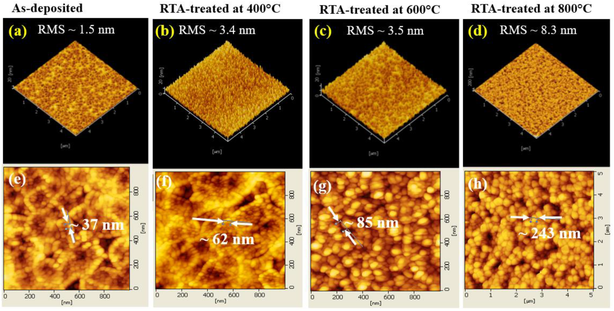
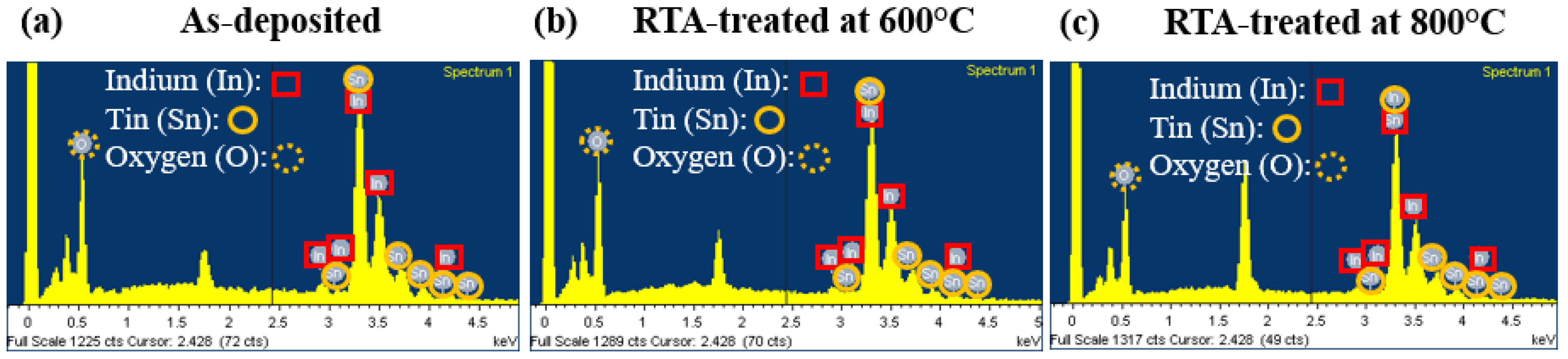
3.1. Sturcture, Surface Morphology and Composition

In Figure 1a, we present the SEM image of the top view of the as-deposited ITO thin film, revealing a smooth surface morphology. Previously, Franz et al. [78] showed that their ~300 nm-thick RF-sputtered ITO films exhibited similar topology to ours, with no apparent grain growth. By enlarging the film thickness to ~30,000 nm, these workers found the film composed of the typical columnar structure with a mean diameter of 140 nm. Working backwards by modeling the columns as tapers with the acute point on the substrate, the diameter of the grains at the surface of ~300 nm-thick ITO film was estimated to be between 10 and 25 nm, as confirmed by independent focused ion beam studies. Using a deposition system and parameters like we employed, Yüzüak and Coşkun [79] reported a topology of as-deposited ITO films that resembles that of ours (Figure 1a). Their X-ray diffraction studies show that the as-deposited film is amorphous. Therefore, we hypothesized that our as-deposited ITO film either is amorphous or consists of nanocrystals with dimensions of this order.
Figure 1c,e illustrate the surface morphology of the ITO thin films processed by RTA at 400 °C and 600 °C, respectively. The two are quite similar and yet clearly distinguishable from the as-deposited film. Notably, a remarkable change in surface morphology of the ITO thin film treated with RTA at 800 °C occurred, as depicted in Figure 1g, where prominent but non-uniform particles are evident. From image analysis of the SEM pictures (ImageJ, University of Wisconsin-Madison, Madison, WI, USA), we estimate that the average areas of grains are 80 nm2, 175 nm2 and 694 nm2 for those annealed at 400 °C, 600 °C and 800 °C, respectively. The corresponding lateral grain sizes are 5 nm, 7.5 nm and 15. 8 nm. The results indicate a significant increase in grain sizes of the ITO thin films as the RTA temperature increases from 400 to 800 °C, a phenomenon also observed in the work of Maniyara et al. [51], who studied the RTA of ITO films at annealing temperatures from 350 to 850 °C. Our values are in general agreement with the crystallite sizes determined using XRD analysis by Chauhan et al. [80] (400 °C: 12 nm) and Stroescu et al. [81] (600 °C: 11 nm), yet are slightly smaller than those reported by Song et al. [49] (400 °C: ~21 nm; 600 °C: ~24 nm). The film thickness of our as-deposited ITO film is 275 ± 6 nm, according to the cross-sectional SEM picture of the film. This is shown in Figure 1b. The thickness of the ITO thin films RTA-treated at 600 °C and 800 °C are 273 ± 3 nm and 273 ± 2 nm, respectively. The corresponding cross-sectional SEM images are shown in Figure 1f,h. These are almost the same as but just slightly thinner than the as-deposited one. This reduction in thickness after annealing may be attributed to the minimization of defects or an increase in density of surface area to volume ratio [82,83]. The cross-sectional SEM view the post-annealed ITO thin film treated with RTA at 400 °C is not available (specified by N/A in Figure 1d). Judging from the observed trend, its thickness should be close to that of the other annealed films in this study. While we did not perform X-ray Diffraction (XRD) measurements, it is highly plausible that our samples, as-deposited one is amorphous while annealed ones are polycrystalline. Using XRD analysis, Song et al. [49], Chauhan et al. [80] and Stroescu et al. [81] reported that ITO thin films crystallized when subjected to RTA for 60 s in a nitrogen environment at 600 °C, 600 °C and 400 °C, respectively. It is worth noting that fully crystalline ITO thin films with a thickness of 300 nm are achievable with RTA treatment at relatively low temperatures of 300 °C for 15 min in an argon environment [84]. This suggests that lower annealing temperatures necessitate increased annealing times to achieve the crystallite ITO films.
AFM was employed to determine the surface roughness and particle size of the ITO thin films. Figure 2a–d display the 3-D top view of the samples under study by AFM. The root mean square (RMS) roughness of the as-deposited ITO film is 1.5 nm, whereas those of the RTA-treated ITO films at 400 °C, 600 °C and 800 °C are 3.4, 3.5 nm and 8.3 nm, respectively. The increasing surface roughness with increasing annealing temperature is consistent with those reported in the literature, e.g., Song et al. [49]. Note that the RMS roughness for RTA-treated ITO thin films at 400 °C and 600 °C is nearly the same. This is also in agreement with the work of Song et al. [49].
We also studied the surface topology of the films using AFM, as shown in Figure 2e–h. The calculated particle sizes (or diameters) of the as-deposited, RTA-treated at 400 °C, RTA-treated at 600 °C and RTA-treated at 800 °C ITO thin films are 37 nm, 62 nm, 85 nm and 243 nm, respectively. The trend of particle size increasing in AFM images with annealing temperature has also been observed by other groups [84]. We note that the AFM topological study revealed particle areas (3020 nm² at 400 °C, 5676 nm² at 600 °C and 46,395 nm² at 800 °C) much higher than those obtained with SEM. This discrepancy is likely due to the particles detected by AFM comprising multiple crystallites or grains as measured with SEM (Figure 1). Other authors have also reported that sputtered ITO films exhibit a domain–subgrain structure where all subgrains in a domain (up to 500 nm diameter) have the same crystallographic orientation [85,86]. Another reason is the resolution difference between AFM and SEM. For instance, Brintlinger et al. [87] found that the image diameter of nanotubes measured by AFM was 50–100 nm, significantly larger than the actual diameter of 1–5 nm measured by SEM.
Energy-dispersive X-ray spectroscopy (EDS) was utilized on the top surface for the elemental analysis of the samples of interest. Figure 3a–c show the EDS spectra, confirming the presence of all related elements, i.e., indium (In), tin (Sn) and oxygen (O). Furthermore, the weight and atomic percentages of all elements recorded by EDS for these samples are displayed in Table 1. The EDS spectroscopic study of RTA-treated ITO thin film at 400 °C is not available.
We note a trend of increasing weight and atomic percentage of oxygen (O), from the ITO samples that were as-deposited (weight: 22.78%, atomic: 68.01%) to RTA-treated at 600 °C (weight: 22.98%, atomic: 68.23%) to RTA-treated at 800 °C (weight: 24.71%, atomic: 70.27%). This trend is suspected to be due to the increasing oxygen partial pressure in the environment, although we performed RTA in a nitrogen atmosphere. Similar phenomena were reported in spinel-type nickel manganite oxide (NiMn2O4-δ) polycrystalline samples treated at high temperatures of 800 °C [88]. On the other hand, indium (In L) produced higher values in both weight (69.48%) and atomic (28.75%) percentages in RTA-treated ITO samples at 600 °C compared to the as-deposited ones (weight: 67.44%, atomic: 28.05%). In contrast, tin (Sn L) exhibited lower values in both weight (7.54%) and atomic (3.02%) percentages in RTA-treated ITO samples at 600 °C compared to the as-deposited ITO thin film (weight: 9.77%, atomic: 3.93%). In related studies by Thirumoorthi et al. [89] and Seki et al. [90], the resistivity of the ITO film was lower, carrier concentration was higher and mobility also increased with increasing Sn L concentrations due to the valence difference between Sn L and In L ion ions. Thus, we expect ITO films that were RTA-treated at 600 °C to be more conductive compared to the as-deposited and RTA-treated at 800 °C ITO thin film. As we shall see later, the trends for mobility and carrier concentration in annealed ITO films are more complex, even though the resistivity of RTA processed at 600 °C is indeed lower.

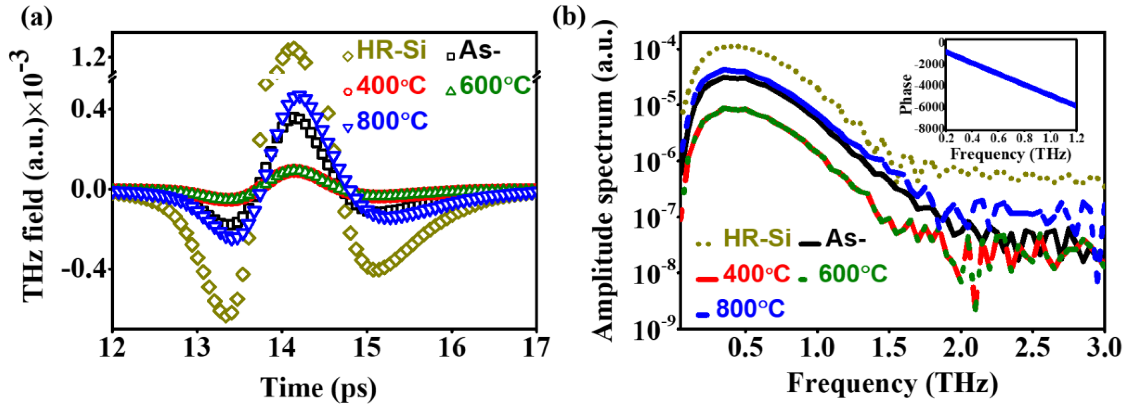
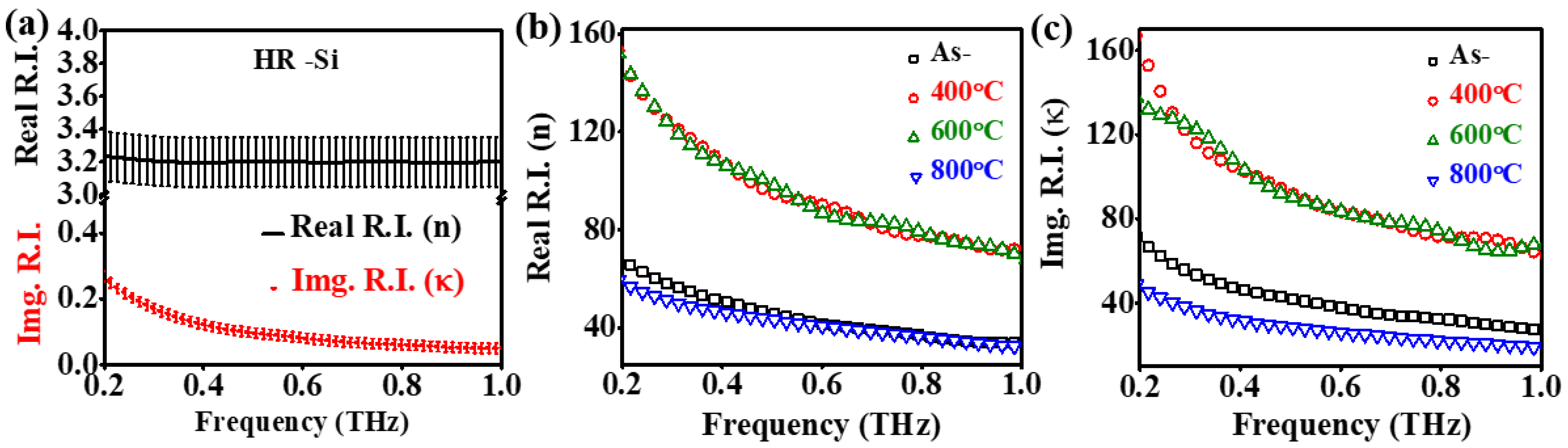
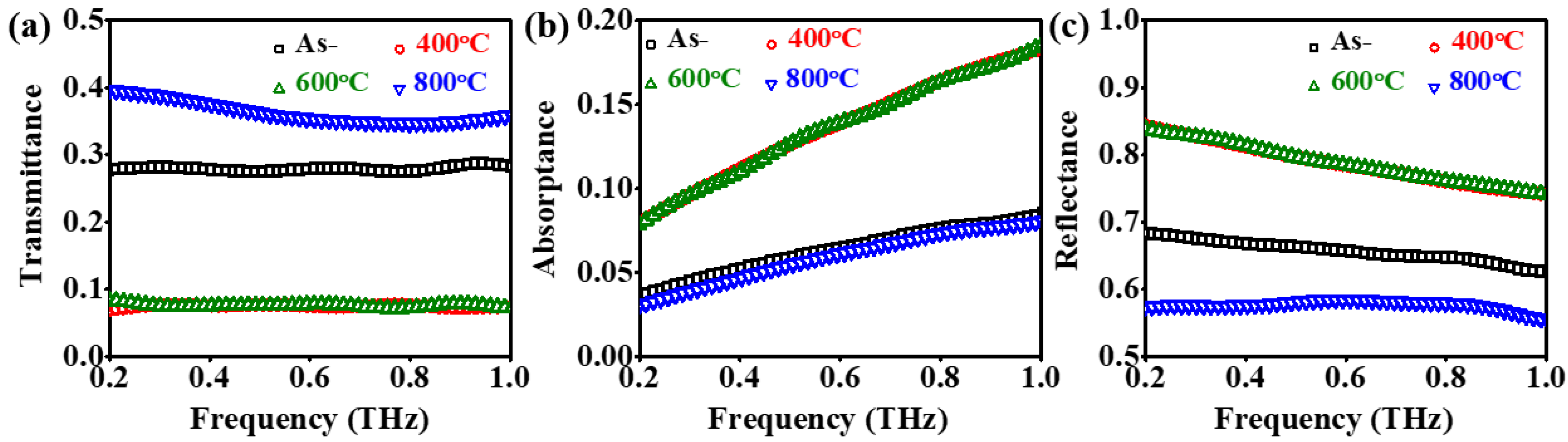
3.2. THz Optical and Electrical Properties

The THz optical properties of as-deposited and RTA-treated ITO thin films coated onto HR silicon and the reference (bare HR silicon) were studied using a homemade transmission-type THz-TDS system. The THz pulse waveforms transmitted through the reference and ITO/HR silicon samples are shown in Figure 4a. A short time delay due to discernible phase shift as well as attenuation of the THz pulse traversing the samples under study can readily be seen. Next, a fast Fourier transform (FFT) algorithm was applied to convert the THz time-domain signal to its spectral amplitudes. These are displayed in Figure 4b. The data, i.e., time-delay or phase shift and attenuation, imply significant interaction between the THz wave and materials investigated. The inset of Figure 4b shows an example of a nearly perfect phase linearity of transmitted THz wave through all the samples in the frequency range from 0.2 to 1.2 THz.
For extraction of the optical constants, we employ the same approach as in our previous works on various thin films and nanostructures [55,56,57,58,59,91,92]. We reiterate here for the benefits of readers: Consider the ITO layer (subscripted as 2) to be sandwiched between air (subscripted as 1) and a substrate (subscripted as 3) with complex refractive indices n2, n1 and n3, respectively. The THz wave is assumed to be incident on this thin layer with a thickness of d from the air toward the substrate. Considering multiple reflections [93], the transmitted THz electric field through the ITO-coated substrate can be written as
E s i g ( ω ) = t 31 E 0 ( ω ) t 12 t 23 e i n 2 ω d c 1 r 21 r 23 e i 2 n 2 ω d c e i n 3 ω D c
where E0, t12, t23, t31, r21 and r23 are the incident electric field, transmission and reflection coefficients between various interfaces; ω is the angular frequency of the THz wave; c is the speed of the light in vacuum; D is the thickness of substrate. Similarly, a reference THz field defined as the THz field transmitted through the bare substrate can be written as
E r e f ( ω ) = t 13 t 31 E 0 ( ω ) e i ω d + n 3 ω D c
The transfer function of the THz wave through the ITO layer then can be written as
E t h e o ( ω , n 2 ) = E s i g ( ω ) E r e f ( ω ) = t 12 t 23 e i ( n 2 1 ) ω d c t 13 1 r 21 r 23 e i 2 n 2 ω d c
Experimentally, texp(ω, n2) is obtained from ratios of the frequency components of the Fourier transforms of the measured THz waveforms through the as-deposited and annealed ITO/HR-Si and the bare substrate. An error function Error(ω, n2) is defined as follows:
t exp ( ω , n 2 ) t t h e o ( ω , n 2 ) = E r r o r ( ω , n 2 )
By minimizing the error function, the real and imaginary parts of the complex refractive index n2 of the thin film layer can be deduced.
Figure 5a shows the real (n) and imaginary (κ) part of refractive indices of the substrate (HR-Si) in the frequency range from 0.2 to 1 THz. The calculated values of n ~3.2 ± 0.18 is nearly constant across the THz frequency band. The value is comparable to that reported by Li et al. [94] and slightly lower than those reported by Dai et al. and others [95,96,97]. On the other hand, the calculated κ slowly decreases from 0.24 to 0.05 with the frequency increasing from 0.2 to 1 THz. This trend closely resembles that reported by Li et al. [94]. Figure 5b,c show the real and imaginary parts of the complex refractive index, n and κ of as-deposited and RTA-treated ITO films at 400 °C, 600° and 800 °C as a function of frequency. In the frequency range of 0.2–1.0 THz, as-deposited ITO thin film exhibits a decreasing trend in n from ~65 to ~33, while κ varies from ~66 to ~27. Such decreasing trends and values of optical constants for as-deposited ITO thin film are very close to those of the DC magnetron-sputtered and electron beam-deposited ITO thin films reported previously by us [55,56,57,58,59] as well as pulsed laser-deposited ITO thin film reported by Wang et al. [60]. This implies that the THz optical constants of ITO films deposited by various methods are very similar. Note that n ≈ κ throughout this frequency band. This implies that the real part of the dielectric constant is very small, since Re [ε] = n2κ2. The dielectric response of the material at THz frequencies is thus dominated by the imaginary part of the dielectric constant.
The THz optical constants of RTA-treated ITO thin films also exhibit an analogous decreasing trend with increasing frequency. Note, however, that the n and κ of ITO films RTA-treated at 400 °C and 600 °C are similar in magnitude and trend. For example, n for the former (Ta = 400 °C) varies from ~143 to ~72 and the latter (Ta = 600 °C) from ~143.4 to ~68, respectively, over the frequency band of 0.2–1.0 THz. The extinction coefficients of ITO films RTA-treated at 400 °C and 600 °C, κ, varies from ~153 to ~64 for the former (Ta = 400 °C), as compared to ~132 to ~68 for the latter (Ta = 600 °C) in the same frequency band. These values are much higher in comparison to those of the as-deposited ITO thin film. In contrast, the n values of RTA-treated at 800 °C ITO thin film revert back to about the same values as those of the as-deposited sample, while its κ is somewhat lower, ranging from ~45 to ~19. These trends can be understood by examining the electric characteristics of the films such as carrier concentration and mobility, which are extracted from the THz optical constants determined above.
The complex THz conductivity, or optical conductivity in the THz band, σ* is related to the dielectric function, ε(ω) = [n(ω) + (ω)]2 through
σ ( ω ) = σ r + i σ i = i ω ε 0 ( ε ε * )
where ε0 is the free-space permittivity and ε~4 is the high-frequency dielectric constant of ITO [58,98,99], consisting of contributions from bound electrons. Therefore, we can determine THz conductivities of samples under study from their complex refractive indices, i.e.,
σ r = ω ε 0 ε i = 2 n κ ω ε 0
σ r = ω ε 0 ( ε ε r ) = ω ε 0 ( ε n 2 + κ 2 ) .
Conversely, the complex optical constants can also be written in terms of the complex conductivity.
In degenerate semiconductors such as ITO, the Drude free-electron model has been most widely used to describe its electrical characteristics. That is, σ * ( ω ) = ε 0 ω p 2 τ ( 1 i ω τ ) [100], where ωp = Nc e2τ/m* and τ is the unscreened plasma frequency and scattering time of carriers in the material; Nc, e and m* = 0.3 m0 [101] are free-electron concentration, electronic charge and effective mass of the electron, respectively, whereas m0 is the electron mass. The real part of the THz conductivity, Re{σ}, exhibits a maximum at zero (DC) frequency and its value decreases with increasing frequency. For Im{σ} [55,56,57,58,59], it can only be positive and approaches a maximum as the frequency approaches that of the inverse of the scattering rate. We have found, however, that the THz conductivities of ITO films and nanostructures exhibit non-Drude-like behavior, e.g., depressed values of DC conductivity and negative values for Im{σ} [55,56,57,58,59]. Therefore, a more generalized conductivity model such as the Drude–Smith model [102], which considers the carrier localization effect, can be considered to describe THz conductivity of the ITO material, In this model,
σ ( ω ) = N c e 2 τ / m 1 i ω τ [ 1 + c 1 i ω τ ]
where c is a fitting parameter that depicts the persistence of velocity of free electrons in the material and can be associated with the degree of backscattering that a carrier suffers after a collision. The values of c is set to vary in the range from −1 to 0 and when c = 0, scattering of free electrons is isotropic and the Drude model is recovered. Within the other limit, i.e., c = −1, carriers undergo complete backscattering or localization. This simple empirical model works remarkably well for a variety of materials and nanostructures [55,56,57,58,59,103]. The mechanisms for carrier localization in ITO films can be either backscattering from grain boundaries [104] or the impurity ions [105].
The unscreened plasma frequency and scattering time together with the c-parameter are judiciously varied to fit the dielectric constants, i.e., optical constants from the THz-TDS data of the samples under study. The electrical parameters such as carrier concentration, mobility, conductivity and resistivity using the following well-known relations: ρ = 1 / σ D C , σ D C = σ ( 0 ) = ( 1 + c ) e N c μ = ( 1 + c ) N c e 2 τ m * = ( 1 + c ) ε 0 ω p 2 τ and μ = ( 1 + c ) e τ m * . For the Drude model, c = 0 in the above.
As we can see in Figure 6, the Drude–Smith model fits the THz conductivity data better than the simple Drude model. All the fitting parameters as well as the electrical parameters deduced are summarized in Table 2, where we have listed instead the screened plasma frequency, ωp* = ωp/(ε)1/2, ε ≈ 4 for ITO [53,106]. The values of ε and m* varied somewhat in the literature. Recent work showed that both are dependent on carrier concentration. Fujiwara and Kondo [107] showed that ε decreases while m* increases with increasing carrier concentration in the range of 1019 to 1021 cm−3. This is confirmed in a recent study by Blair et al. [108]. Here we assumed that both are constants, independent of carrier concentration. This can introduce ambiguity in the extracted electrical parameters.
Previously, we have shown that THz-TDS analysis yield electrical parameters, e.g., the DC conductivity, that provide reasonable estimates to those obtained by Hall measurements [55]. Similar observations were made by Brown et al. [109], the deviation being attributed by the observation that ITO is non-Drude-like and surface roughness. Mergel and Qiao [85] observed that the “optical” conductivity and mobility in ITO films are generally higher than their corresponding electrical parameters. This discrepancy is due to pronounced microstructures with poorly conducting grain boundaries, which reduce DC conductivity but do not hinder the oscillatory motions of optically excited carriers. Uprety et al. [54] also stated that the inclusion of THz range data for spectroscopic ellipsometric measurement is necessary to achieve good agreement with conventional direct current approaches such as measurements done by Hall or 4-point probe instruments. Examining Table 2, we find that the resistivity of the ITO film first drops to 2.0 × 10⁻⁴ Ω‧cm as the annealing temperature was raised to 400 °C and 600 °C, then becomes higher for Ta = 800 °C, reaching 15.9 × 10⁻⁴ Ω‧cm, somewhat higher than that of the as-deposited film, 9.8 × 10⁻⁴ Ω‧cm. Since the optical constants of ITO films are closely related to resistivity or conductivity, the dependence of n and κ on Ta shown in Figure 5 can now be qualitatively understood.
Rapid thermal annealing is expected to (i) substitute more In3+ by Sn4+, (ii) create more oxygen vacancies and (iii) enlarge the grain (Figure 1 and Figure 2) with reduced density of grain boundaries to create freer and more mobile charge carriers. As a result, the mobility and carrier concentration of the annealed films are expected to be higher. Previously, A. Valla et al. [110] identified the role of various scattering mechanisms that limit the mobility of ITO films for a range of carrier concentrations. If the carrier concentration (Nc) in the film is less than 2 × 1019 cm−3, then the mobility is adversely affected by the grain boundaries’ scattering mechanism. Scattering by ionized/neutral impurities, on the other hand, can play a dominant role in the reduction of the mobility value if the ITO film contains high carrier concentration (Nc > 2 × 1020 cm−3). This is indeed the case for annealed ITO films treated at Ta = 400 and 600 °C. Several other groups have reported similar findings. In their work on RTA-treated ITO films with Ta between 500–950 °C, Parida et al. [111] observed a plateau region for resistivity of their samples at Ta = 500–600 °C. Upon further increasing of annealing temperature, ρ first drops but becomes higher for Ta ≥ 850 °C. The authors argued that the structure of ITO annealed at relatively high temperatures are unstable, with ρ, μ and Nc co-related to each other due to the formation of oxygen interstitials and Sn-related defect centers. Studying the annealing temperature from 100 to 550°C, Yuan et al. [112] found that the resistivity of annealed ITO film RTA in vacuum rapidly decreases until about 450°C, reaching a minimum of 2.5 × 10⁻⁴ Ω-cm at 450 °C. Further increasing the annealing temperature, the resistivity rises to 4.5 × 10⁻⁴ Ω-cm at 550 °C. Ahmed et al. [38] also observed that furnace-annealing at 550 °C input excess heat that adversely affects the film structure by creating voids between the grains. In a study to extend the NIR transmission window of ITO films by RTA at various temperatures starting from 350 °C to 850 °C, Maniyara et al. [51] also observed that the sheet resistance of the film decreased with increasing annealing temperature up to 750 °C but increased abruptly above that point. Sun et al. [113] studied effects of ambient high-temperature annealing (700–1000 °C) on the electrical properties of ITO films. Increased resistivity at elevated temperatures was thought to be due to adsorbed oxygen molecules occupying positions of oxygen vacancies. Consequently, carrier concentration sharply decreased when we performed annealing in a nitrogen atmosphere. Residual oxygen desorbed from the RTA chamber cannot be ruled out. The findings of these groups are consistent with what we observed and are correlated with values of c-parameters of the samples shown in Table 2: −0.83 and −0.87 for as-deposited and heat-treated ITO films at 800 °C and −0.68 and −0.67 for annealed ITO films at 400 °C and 600 °C. Such values of the c-parameter suggest the presence of strong scattering centers like grain boundaries and ionized impurities, i.e., oxygen vacancies and Sn+4 substitutions. Backscattering is stronger for as-deposited and RTA-processed ITO films at 800 °C than annealed ITO films at 400 °C and 600 °C. As a result, the mobility for the former two is lower. Insights can also be gained by examination of some relevant length scales. The mean free path of carriers, Lfree, can be estimated as [104]
L f r e e = v t h e r m a l τ = ( 3 k B T τ 2 / m * ) 1 / 2 ,
where kB = 1.381 × 10⁻²³ J⋅K−1 is the Boltzmann constant, T = 300 K is the temperature of the samples in Kelvin and νthermal is the thermal velocity from classical equipartition of energy. Using the above values and the scattering times, τ, in Table 2, Lfree of samples under study are estimated to be 1.28 nm, 2.56 nm, 4.48 nm and 4.26 nm, respectively, for as-deposited and RTA-treated ITO films at 400 °C, 600 °C and 800 °C, respectively. From SEM studies (see Figure 1), we show that the lateral grain sizes for annealed samples are 5 nm, 7.5 nm and 15. 8 nm, respectively. Hence, the mean free path is comparable to the grain sizes in our samples. As a result, scattering of carriers by grain boundaries is expected to be significant. Further, the charged impurity (Tin) scattering centers in ITO will also enhance the localization of carriers [105,114]. The average distance between dopant ions is proportional to the inverse of the third root of doping concentration. Therefore, free electrons will run into the dopant ions easily if the doping concentration is high enough. The average distance between dopant ions can be estimated from (Nc)−1/3 or 9.95 nm, 9.26 nm, 11.84 nm and 38.93 nm for as-deposited and RTA-treated ITO films at 400 °C, 600 °C and 800 °C, respectively. Consequently, free carriers are unlikely to run into such scattering centers in the length of one mean free path. Therefore, carrier scattering by impurity ions are expected to play a minor role in our samples.
The transmittance of samples under study was calculated using the ratio of measured frequency-domain THz field amplitudes through the ITO/HR silicon to that through the reference (bare HR silicon); see Figure 7a. The THz transmittance of as-deposited and RTA-treated ITO thin films are slow-varying in the band of 0.2–1.0 THz. The average transmittance of as-deposited and RTA-treated ITO films at 400 °C, 600 °C and 800 °C are 27%, 8%, 8% and 39%, respectively. We note the average THz transmittance of as-deposited ITO thin film is somewhat lower than those thinner (~100 nm) as-deposited ITO thin films (T ~40%) used in our earlier device works [68]. This is primarily attributed to the thickness-dependent free carrier absorption of ITO thin films. The THz transmittance of ITO thin film treated with RTA at 400 °C and 600 °C are as low 8%. This is consistent with higher extinction coefficients of RTA-annealed ITO films at either 400 °C or 600 °C shown in Figure 5b. Our results indicate that annealing temperature is a critical parameter affecting transmittance and reflectance of the ITO film in the THz band.
In Figure 7b,c, the absorptance and reflectance of ITO thin films depend strongly on the annealing temperature in this frequency band. Here, the absorptance A ≈ αd, where the absorption coefficient α is related to the extinction coefficient κ by α = 4πκ/λ. In turn, reflectance of the samples is given by R = 1-T-A. We note that the decreasing trend of reflectance with frequency and dependence on conductivity or resistivity is consistent with the Hagen–Rubens relation [70,115], R ( ω ) = 1 2 2 ϵ 0 ω / σ , . Both absorptance and reflectance are found to be much higher for ITO films heat-treated by RTA at 400 °C and 600 °C than that of as-deposited ones. This suggests that RTA-treated ITO thin films at either 400 °C or 600 °C could potentially be useful as dichroic mirrors or absorbers for the THz band [70,116]. On the other hand, ITO thin films RTA-treated beyond 800 °C could be an effective THz TCE material for THz photonic devices. We note the transmittance of ITO-coated device can be further enhanced by employing a grating-like, i.e., wire-grid, structure, as we have demonstrated earlier [68].

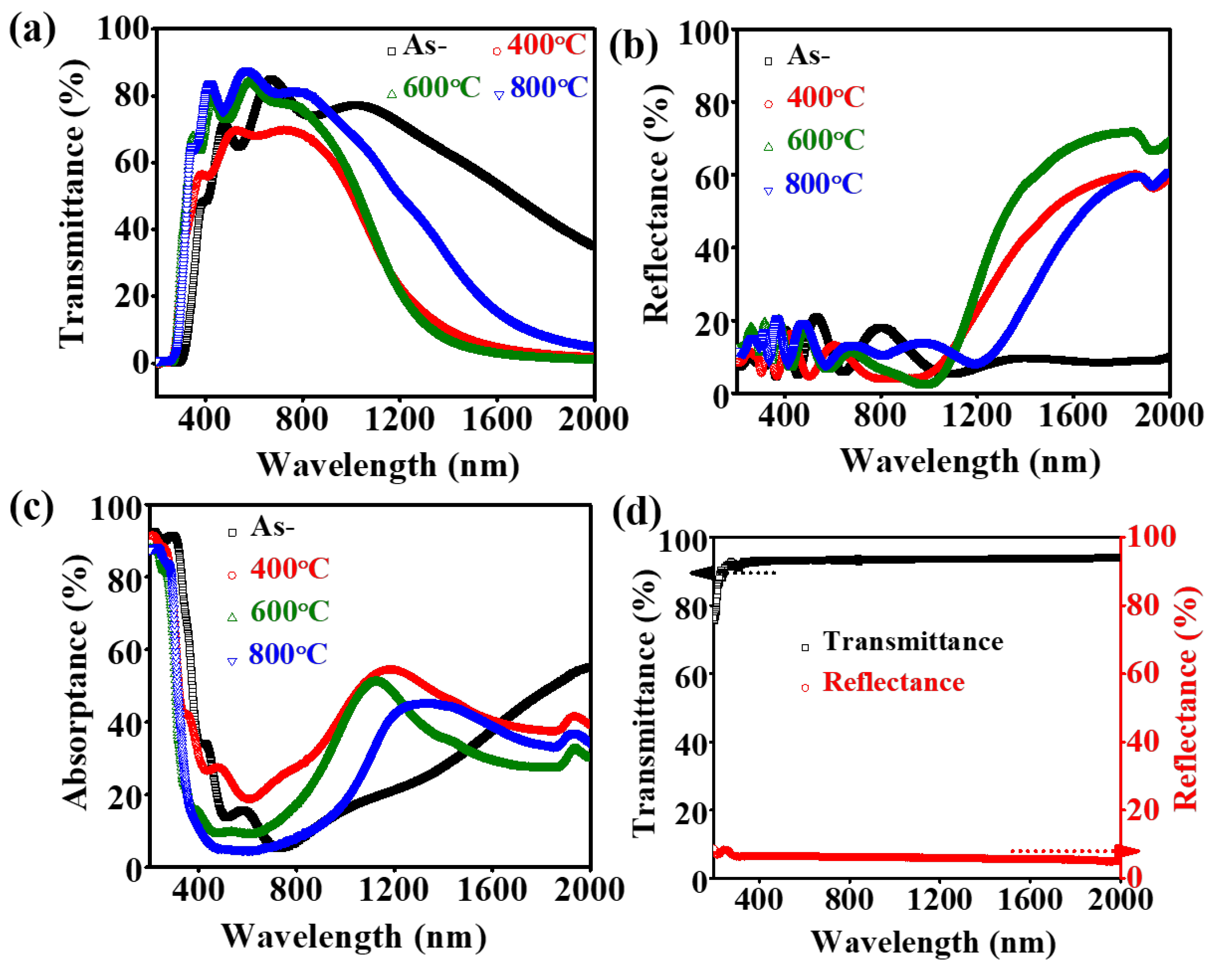
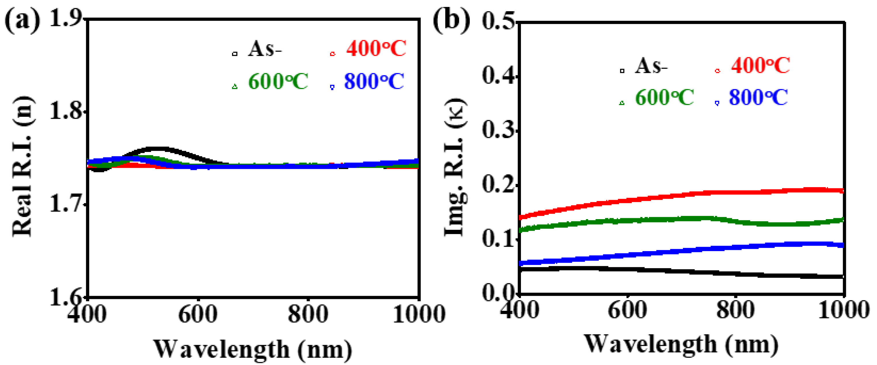
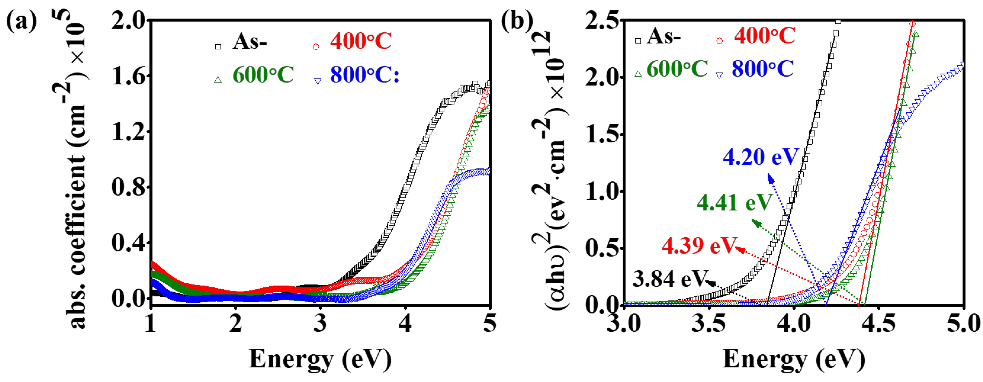
3.3. Annealing Effects on UV-VIS-NIR Optical Properties of ITO Films

It is interesting to compare the optical properties of ITO films fabricated and processed for this work in the ultraviolet (UV), visible (VIS) and near-infrared (NIR) band as a bearing on their optical properties in the far infrared (FIR) or THz frequency range. We have experimentally measured transmittance and reflectance of as-deposited and RTA-treated ITO thin films coated onto fused silica as well as those of the substrate itself in the energy range of 0.6 eV–6 eV, or the wavelength band of 200–2000 nm. These are shown in Figure 8. The average transmittance in the VIS-NIR region (400–800 nm) band for as-deposited ITO film was Tav ~72%. After annealing at 400 °C, 600 °C and 800 °C, Tav was ~68%, ~80% and 83%, respectively. Considering the contribution by the substrate (see Figure 8d), all samples can be considered highly transparent. Higher transmittance of samples after heat treatment by annealing can be attributed to increasing sizes of crystallites after annealing, as shown in the SEM data (see Figure 1). It is well known that improved crystallinity leads to reduced scattering of incident light in the transparency window. Thus transmission of visible light through the film is higher. Transmittance drops off sharply in the NIR and UV band for all samples. The positions of the band gap or onset of absorption shifted to shorter wavelength for samples annealed at increasingly higher temperatures. This point will be addressed in more detail later on in this subsection.
The average reflectance of as-deposited ITO thin film in the visible band (400–800 nm), Rav ~14%. Whereas, the average reflectance of ITO thin film RTA-treated at 400 °C, 600 °C and 800 °C are ~10%, ~12% and ~13%, respectively, in this transparency window. In addition, the reflectance curves show small yet significant oscillations due to multiple reflections of light within the sample. This is also in reasonably good agreement with previous findings by others [117]. Further, annealed samples show higher reflectivity in the NIR region [118,119], approaching the plasma edge. The highest NIR reflectivity, ~70% was attained by the ITO film annealed at 600 °C. We tentatively attributed this to the high carrier concentration in this sample; see Table 2 for a tabulation of carrier concentration for all samples. Note that the reflectivity is slightly lower for the ITO thin film RTA-treated at 800 °C. This correlates with the lower carrier concentration found in this sample, which also exhibits the highest surface roughness of all samples [120]. The position of the plasma edge and steepness of reflectance curves in the NIR for the annealed samples is related to its post-annealing carrier concentration and mobility [85,121]. Compared with Figure 7, we note that the transmission properties of as-deposited and RTA-annealed ITO films in the visible transparency window and the THz band are somewhat different. This could be understood by realizing that ITO films are dielectric-like in the visible spectrum and metal-like in the far-infrared.
We now focus on spectral regions of ITO films that are weakly absorbing and have also shown prominent maximum (TM) and minimum (Tm) transmission spectrum, i.e., the visible window of 400–800 nm (see Figure 8a). Following Swanepoel [122], the refractive index of ITO the film in its weakly absorbing VIS-NIR (400 to 1000 nm) band can be written as n = [ N + ( N 2 n s u b 2 ) 1 / 2 ] 1 / 2 , where N = 2 n s u b T M T m T M T m + n s u b 2 + 1 2 , TM and Tm are envelopes of maxima and minima of the transmission curve, whereas n s u b = 1 + ( 1 T 2 ) 1 / 2 T is the refractive index of fused silica substrate and is determined using its transmission spectrum (T) to be ~1.43 and found to be fairly independent of wavelength. The calculated refractive index n of as-deposited and RTA-treated ITO thin films in wavelength range from 400 to 1000 nm are shown in Figure 9a. Note that the refractive index of 1.74 in this band is almost wavelength-independent and approximately the same for all types of ITO thin films studied in this work. In the literature, the reported refractive indices for as-deposited as well as annealed ITO thin films vary from 1.6 to 2 within this band [123].
The thickness d of those ITO thin films can be determined using the envelopes of maxima and minima of the transmission curve in the visible spectra, d = λ 1 λ 2 2 ( λ 1 n 2 λ 2 n 1 ) , where n1 and n2 are the refractive indices at two adjacent maxima or minima, TM or Tm, corresponding to wavelengths at λ1 and λ2, respectively. The estimated thickness of as-deposited and RTA-treated ITO thin films at 400 °C, 600 °C and 800 °C are ~470 nm, ~410 nm, ~483 nm and ~468 nm, respectively. Knowing the thickness of ITO thin films, the absorption coefficient α of these samples are extracted using the relationship between transmittance (T), reflectance (R) and thickness d, given by α = 1 d ln ( 1 R ) 2 2 T + ( 1 R ) 4 4 T 2 + R 2 . Next, the imaginary part of refractive index κ as the function of wavelength is evaluated using the relati κ = α λ / 4 π . This is plotted in Figure 9b. We found that κ in the wavelength range of 400 to 1000 nm is small and slow-varying and approximately 0.04, 0.18, 0.13 and 0.07 for as-deposited and RTA-treated ITO thin films at 400 °C, 600 °C and 800 °C, respectively. Such estimated values are also in agreement with those reported in previous works [123].
Crystalline ITO has been shown to be a direct gap semiconductor [124]. From the absorption coefficient α as plotted in Figure 10a, the optical bandgap Eg or the onset of absorption can be extracted using the extrapolation method proposed by Tauc: (αhʋ)2 = A (hʋ-Eg) [125]; where A is a constant and h = 6.626 × 10⁻³⁴ J.s is the Planck constant. These are shown for the samples under study in Figure 9b. The optical band gap Eg of as-deposited ITO thin film was found to be 3.84 eV, which broadened for RTA-treated ITO thin films at 400 °C, 600 °C and 800 °C to 4.39 eV, 4.41 eV and 4.2 eV, respectively. The basic physics of this phenomenon is the carrier–concentration dependence of Eg, i.e., the Burstein–Moss effect [126,127] and band gap shrinkage or renormalization due to electron-electron and electron-ionized impurity scattering [5,53,128]. Our values are in a good agreement with typical value reported previously. For example, Abd-Elnaiem et al. [129], extracted Eg for as-deposited and annealed ITO thin films with thickness of ~80 nm at 300 °C to be ~3.2 eV and~3.8 eV, respectively. Meanwhile, Eg for a 200 nm-thick ITO films heat-treated with RTA at 600 °C was reported to be 4.04 eV by Song et al. [49]. We note the band gap of ITO thin films increases by 0.57 eV after RTA treatment at 600 °C. This aligns with observation of Park et al. [130], who reported a 0.60 eV shift after furnace annealing at 400 °C for their 150 nm-thick ITO films.

4. Conclusions

In this study, we explored the manipulation of optical properties of radio frequency (RF)-sputtered indium tin oxide (ITO) thin films on highly resistive silicon substrate by rapid thermal annealing (RTA) in the terahertz (THz) frequency band. The optical constants of as-deposited and RTA-processed ITO films annealed at 400 °C, 600 °C and 800 °C are determined by THz time-domain spectroscopy (THz-TDS). The THz optical constants of RTA-treated ITO thin films are shown to exhibit a decreasing trend with increasing frequency. In contrast, the n values of RTA-treated at 800 °C ITO thin film revert back to about the same values as those of the as-deposited sample. These trends can be understood by examining the electric characteristics of the films such as carrier concentration and mobility. The real (n) and imaginary (κ) refractive indices of ITO films RTA-treated at 400 °C and 600 °C are similar in magnitude. For example, n for the former (Ta = 400 °C) varies from ~143 to ~72 and the latter (Ta = 600 °C) from ~143.4 to ~68, respectively, over the frequency band of 0.2–1.0 THz. The extinction coefficients of ITO films RTA-treated at 400 °C and 600 °C, κ, varies from ~153 to ~64 for the former (Ta = 400 °C), as compared to ~132 to ~68 for the latter (Ta = 600 °C) in the same frequency band. Their values, are much higher in values in comparison to those of the as-deposited ITO thin film, which exhibits a decreasing trend in n from ~65 to ~33, while κ varies from ~66 to ~27. In contrast, the n values of RTA-treated ITO films at 800 °C ITO thin film revert back to about the same values as those of the as-deposited sample, while its κ is somewhat lower, ranging from ~45 to ~19.
The transmittance can be changed from ~27% for as-deposited to ~10% and ~39% for ITO films heat-treated at different annealing temperatures, Tas. RTA-treated ITO thin films at either 400 °C or 600 °C could potentially be useful as dichroic mirrors or absorbers for the THz band. On the other hand, ITO thin films RTA-treated beyond 800 °C could be an effective material as transparent conducting electrodes (TCE) for THz EO devices. We note the transmittance of ITO-coated device can be further enhanced by employing a grating-like, i.e., wire-grid, structure, as we have demonstrated earlier. Such variations of optical properties in the far infrared for the samples under study are correlated with their mobility and carrier concentration, which are extracted from Drude–Smith modeling of THz conductivity with plasma frequency, scattering time and the c-parameters as fitting parameters. Resistivities of the films are in the range of 10−3 to 10−4 Ω-cm, confirming that annealed ITO films can potentially be used as transparent conducting electrodes for photonic devices operating at THz frequencies. The highest mobility, μ = 47 cm2/V∙s, with carrier concentration, Nc = 1.31 × 1021 cm−3, was observed for ITO films annealed at Ta = 600 °C. The scattering times of the samples were in the range of 8–21 fs, with c-values of −0.63 to −0.87, indicating strong backscattering of the carriers, mainly by grain boundaries in the polycrystalline film. To better understand the nature of these films, we have also characterized the surface morphology, microscopic structural properties and typical chemical composition of as-deposited and RTA-processed ITO thin films. For comparison, we have summarized the optical properties of ITO films sputtered on fused silica substrates, as-deposited and RTA-annealed, focusing on the visible transparency window and the near-infrared (400–1000 nm). the refractive index of 1.74 in this band is almost wavelength-independent and approximately the same for all types of ITO thin film studied in this work. The extinction coefficient, κ in this band is small and slow varying and approximately 0.04, 0.18, 0.13 and 0.07 for as-deposited and RTA-treated ITO thin films at 400 °C, 600 °C and 800 °C, respectively. The optical band gap Eg’s of as-deposited ITO thin film were found to be 3.84 eV, which broadened for RTA-treated ITO thin films at 400 °C, 600 °C and 800 °C to 4.39 eV, 4.41 eV and 4.2 eV, respectively.
Overall, our study offers valuable insights into leveraging rapid thermal annealing to modify terahertz optical properties of ITO films, with potential applications spanning from coatings for waveguides to terahertz electro-optic switching devices and manipulation of terahertz electromagnetic waves.

Author Contributions

Conceptualization, C.-L.P. and A.K.S.; methodology, C.-L.P. and A.K.S.; software, W.-C.A. and A.K.S.; validation, C.-L.P., A.K.S. and W.-C.A.; formal analysis, C.-L.P., A.K.S. and W.-C.A.; investigation, C.-L.P., A.K.S. and W.-C.A.; resources, C.-L.P.; data curation, A.K.S.; writing—original draft preparation, A.K.S.; writing—revision, C.-L.P.; visualization, C.-L.P.; supervision, C.-L.P.; project administration, C.-L.P.; funding acquisition, C.-L.P. All authors have read and agreed to the published version of the manuscript.

Funding

This research was funded in part by the Ministry of Science and Technology (the National Science and Technology Council), Taiwan, under various grants.

Institutional Review Board Statement

Not applicable.

Informed Consent Statement

Not applicable.

Data Availability Statement

The data presented in this study are available on request from the corresponding author.

Acknowledgments

A.K.S. would like to thank Chia-Ming Mai for THz-TDS measurement. The authors would like to thank Peichen Yu from National Yang Ming Chiao Tung University Taiwan, for use of the UV-VIS-NIR spectrometer. They would also like to thank the Center for Nanotechnology, Materials Science and Microsystems (CNMM), NTHU, where the samples were fabricated. A.K.S. acknowledges the National Science and Technology Council (NSTC), Taiwan, for the fellowship that facilitated postdoctoral research at the Department of Physics, NTHU, Taiwan.

Conflicts of Interest

The authors declare no conflicts of interest.

References

  1. Ellmer, K. Past achievements and future challenges in the development of optically transparent electrodes. Nat. Photon. 2012, 6, 809–817. [Google Scholar] [CrossRef]
  2. Ginley, D.; Hosono, H.; Paine, D. Handbook of Transparent Conductors; Springer: New York, NY, USA, 2010. [Google Scholar]
  3. Chavan, G.T.; Kim, Y.; Khokhar, M.Q.; Hussain, S.Q.; Cho, E.-C.; Yi, J.; Ahmad, Z.; Rosaiah, P.; Jeon, C.-W. A Brief Review of Transparent Conducting Oxides (TCO): The Influence of Different Deposition Techniques on the Efficiency of Solar Cells. Nanomaterials 2023, 13, 1226. [Google Scholar] [CrossRef] [PubMed]
  4. Tripathi, M.N.; Bahramy, M.S.; Shida, K.; Sahara, R.; Mizuseki, H.; Kawazoe, Y. Optoelectronic and magnetic properties of Mn-doped indium tin oxide: A first-principles study. J. Appl. Phys. 2012, 112, 073105. [Google Scholar] [CrossRef]
  5. Hamberg, I.; Granqvist, C.G.; Berggren, K.F.; Sernelius, B.E.; Engström, L. Band-gap widening in heavily Sn-doped In2O3. Phys. Rev. B 1984, 30, 3240–3249. [Google Scholar] [CrossRef]
  6. Li, S.; Tian, M.; Gao, Q.; Wang, M.; Li, T.; Hu, Q.; Li, X.; Wu, Y. Nanometre-thin indium tin oxide for advanced high-performance electronics. Nat. Mater. 2019, 18, 1091–1097. [Google Scholar] [CrossRef] [PubMed]
  7. Yu, Z.; Perera, I.R.; Daeneke, T.; Makuta, S.; Tachibana, Y.; Jasieniak, J.J.; Mishra, A.; Bäuerle, P.; Spiccia, L.; Bach, U. Indium tin oxide as a semiconductor material in efficient p-type dye-sensitized solar cells. NPG Asia Mater. 2016, 8, e305. [Google Scholar] [CrossRef]
  8. Ma, Z.; Li, Z.; Liu, K.; Ye, C.; Sorger, V.J. Indium-tin-oxide for high-performance electro-optic modulation. Nanophotonics 2015, 4, 198–213. [Google Scholar] [CrossRef]
  9. Dhere, R.G.; Gessert, T.A.; Schilling, L.L.; Nelson, A.J.; Jones, K.M.; Aharoni, H.; Coutts, T.J. Electro-optical properties of thin indium tin oxide films: Limitations on performance. Sol. Cells 1987, 21, 281–290. [Google Scholar] [CrossRef]
  10. Shi, K.; Haque, R.R.; Zhao, B.; Zhao, R.; Lu, Z. Broadband electro-optical modulator based on transparent conducting oxide. Opt. Lett. 2014, 39, 4978–4981. [Google Scholar] [CrossRef] [PubMed]
  11. Si, M.; Andler, J.; Lyu, X.; Niu, C.; Datta, S.; Agrawal, R.; Ye, P.D. Indium-Tin-Oxide Transistors with One Nanometer Thick Channel and Ferroelectric Gating. ACS Nano 2020, 14, 11542–11547. [Google Scholar] [CrossRef] [PubMed]
  12. Kim, H.; Gilmore, C.M.; Piqué, A.; Horwitz, J.S.; Mattoussi, H.; Murata, H.; Kafafi, J.H.; Chrisey, D.B. Electrical, optical, and structural properties of indium-tin-oxide thin films for organic light-emitting devices. J. Appl. Phys. 1999, 86, 6451–6461. [Google Scholar] [CrossRef]
  13. Lee, S.; Noh, J.H.; Bae, S.-T.; Cho, I.-S.; Kim, J.Y.; Shin, H.; Lee, J.-K.; Jung, H.S.; Hong, K.S. Indium-tin-oxide-based transparent conducting layers for highly efficient photovoltaic devices. J. Phys. Chem. C 2009, 113, 7443–7447. [Google Scholar] [CrossRef]
  14. Janarthanan, B.; Thirunavukkarasu, C.; Maruthamuthu, S.; Manthrammel, M.A.; Shkir, M.; Al Faify, S.; Selvakumar, M.; Reddy, V.R.M.; Park, C. Basic deposition methods of thin films. J. Mol. Struct. 2021, 1241, 130606. [Google Scholar] [CrossRef]
  15. Laux, S.; Kaiser, N.; Zöller, A.; Götzelmann, R.; Lauth, H.; Bernitzki, H. Room-temperature deposition of indium tin oxide thin films with plasma ion-assisted evaporation. Thin Solid. Film. 1998, 335, 1–5. [Google Scholar] [CrossRef]
  16. Park, S.K.; Jeong, I.H.; Kim, W.K.; Kwak, M.G. Deposition of indium-tin-oxide films on polymer substrates for application in plastic-based flat panel displays. Thin Solid. Film. 2001, 397, 49–55. [Google Scholar] [CrossRef]
  17. Stadler, A. Transparent Conducting Oxides—An Up-To-Date Overview. Materials 2012, 5, 661–683. [Google Scholar] [CrossRef] [PubMed]
  18. Alam, M.J.; Cameron, D.C. Optical and electrical properties of transparent conductive ITO thin films deposited by sol–gel process. Thin Solid Film. 2000, 377, 455–459. [Google Scholar] [CrossRef]
  19. Senthilkumar, V.; Vickraman, P.; Jayachandran, M.; Sanjeeviraja, C. Structural and optical properties of indium tin oxide (ITO) thin films with different compositions prepared by electron beam evaporation. Vacuum 2010, 84, 864–869. [Google Scholar] [CrossRef]
  20. Robb, A.J.; Duca, Z.A.; White, N.; Woodell, P.; Ward, P.A. Influence of oxygen on the optical and electrical properties of magnetron-sputtered indium tin oxide thin films at ambient temperature. Thin Solid Film. 2024, 788, 140152. [Google Scholar] [CrossRef]
  21. Alabdan, H.I.; Alsahli, F.M.; Bhandari, S.; Mallick, T. Monolithic Use of Inert Gas for Highly Transparent and Conductive Indium Tin Oxide Thin Films. Nanomaterials 2024, 14, 565. [Google Scholar] [CrossRef] [PubMed]
  22. Jung, J.; Guo, R. Optimized sputtering parameters for ITO thin films of high conductivity and transparency. Adv. Appl. Electroceramics II Ceram. Trans. 2012, 235, 43–53. [Google Scholar]
  23. Li, M.; Mo, C.; Chen, J.; Ji, P.; Tan, H.; Zhang, X.; CUI, M.; ZHUGE, L.; WU, X.; Huang, T. Effects of power on ion behaviors in radio-frequency magnetron sputtering of indium tin oxide (ITO). Plasma Sci. Technol. 2024, 26, 075506. [Google Scholar] [CrossRef]
  24. Huang, T.; Mo, C.; Cui, M.; Li, M.; Ji, P.; Tan, H.; Zhang, X.; Zhuge, L.; Wu, X. Ion behavior impact on ITO thin film fabrication via DC magnetron sputtering with external anode. Vacuum 2024, 221, 112848. [Google Scholar] [CrossRef]
  25. Zhang, X.; Zhang, G.; Yan, Y. Effects of Doping Ratio and Thickness of Indium Tin Oxide Thin Films Prepared by Magnetron Sputtering at Room Temperature. Coatings 2023, 13, 2016. [Google Scholar] [CrossRef]
  26. Balasubramanian, N.; Subrahmanyam, A. Electrical and optical properties of reactively evaporated indium tin oxide (ITO) films-dependence on substrate temperature and tin concentration. J. Phys. D Appl. Phys. 1989, 22, 206. [Google Scholar] [CrossRef]
  27. Nisha, M.; Anusha, S.; Antony, A.; Manoj, R.; Jayaraj, M.K. Effect of substrate temperature on the growth of ITO thin films. Appl. Surf. Sci. 2005, 252, 1430–1435. [Google Scholar] [CrossRef]
  28. Meng, L.-J.; dos Santos, M.P. Properties of indium tin oxide films prepared by RF reactive magnetron sputtering at different substrate temperature. Thin Solid Film. 1998, 322, 56–62. [Google Scholar] [CrossRef]
  29. Kurdesau, F.; Khripunov, G.; Cunha, A.F.; Kaelin, M.; Tiwari, A.N. Comparative study of ITO layers deposited by DC and RF magnetron sputtering at room temperature. J. Non-Cryst. Solids 2015, 352, 1466–1470. [Google Scholar] [CrossRef]
  30. Yang, S.; Zhong, J.; Sun, B.; Zeng, X.; Luo, W.; Zhao, X.; Shu, Y.; Chen, J.; He, J. Influence of base pressure on property of sputtering deposited ITO film. J. Mater. Sci. Mater. Electron. 2019, 30, 13005–13012. [Google Scholar] [CrossRef]
  31. Meng, L.J.; Dos Santos, M.P. Properties of indium tin oxide (ITO) films prepared by rf reactive magnetron sputtering at different pressures. Thin Solid Film. 1997, 303, 151–155. [Google Scholar] [CrossRef]
  32. Liu, Z.; Liang, J.; Zhou, H.; Sun, H.; Lu, W.; Wang, B.; Li, Q.; Zhao, X.; Wang, D.; Xu, J. Effect of nitrogen partial pressure on the piezoresistivity of magnetron sputtered ITO thin films at high temperatures. Appl. Surf. Sci. 2023, 608, 55292. [Google Scholar] [CrossRef]
  33. Guileen, C.; Herrero, J. Structure, optical and electrical properties of indium tin oxide thin films prepared by sputtering at room temperature and annealed in air or nitrogen. J. Appl. Phys. 2007, 101, 073514–073521. [Google Scholar] [CrossRef]
  34. Hamouda, F.; Herth, E.; David, C.; Bayle, F.; Plante, M.P.; Martin, A.; Aassime, A. Electrical and optical properties of sputtered ultra-thin indium tin oxide films using xenon/argon gas. J. Mater. Sci. Mater. Electron. 2019, 30, 8508–8514. [Google Scholar] [CrossRef]
  35. Kim, Y.; Joo, S.H.; Shin, S.G.; Choi, H.W.; Bark, C.W.; Rim, Y.S.; Kim, K.H.; Kim, S. Effect of Annealing in ITO Film Prepared at Various Argon-and-Oxygen-Mixture Ratios via Facing-Target Sputtering for Transparent Electrode of Perovskite Solar Cells. Coatings 2022, 12, 203. [Google Scholar] [CrossRef]
  36. Baptista, A.; Silva, F.; Porteiro, J.; Míguez, J.; Pinto, G. Sputtering physical vapour deposition (PVD) coatings: A critical review on process improvement and market trend demands. Coatings 2018, 8, 402. [Google Scholar] [CrossRef]
  37. Donercark, E.; Guler, S.; Ciftpinar, E.H.; Kabacelik, I.; Koc, M.; Ercelebi, A.C.; Turan, R. Impact of oxygen partial pressure during Indium Tin Oxide sputtering on the performance of silicon heterojunction solar cells. Mater. Sci. Eng. B 2022, 281, 115750. [Google Scholar] [CrossRef]
  38. Ahmed, N.M.; Sabah, F.A.; Abdulgafour, H.I.; Alsadig, A.; Sulieman, A.; Alkhoaryef, M. The effect of post annealing temperature on grain size of indium-tin-oxide for optical and electrical properties improvement. Results Phys. 2019, 13, 102159. [Google Scholar] [CrossRef]
  39. Seong, S.; Jung YCh Lee, T.; Park, I.-S.; Ahn, J. Enhanced uniformity in electrical and optical properties of ITO thin films using a wide thermal annealing system. Mater. Sci. Semicond. Proc. 2018, 79, 14–19. [Google Scholar] [CrossRef]
  40. Kaźmierczak-Bałata, A.; Bodzenta, J.; Dehbashi, M.; Mayandi, J.; Venkatachalapathy, V. Influence of Post Processing on Thermal Conductivity of ITO Thin Films. Materials 2023, 16, 362. [Google Scholar] [CrossRef]
  41. Shubitidze, T.; Britton, W.A.; Negro, L.D. Enhanced Nonlinearity of Epsilon-Near-Zero Indium Tin Oxide Nanolayers with Tamm Plasmon-Polariton States. Adv. Opt. Mater. 2024, 12, 2301669. [Google Scholar] [CrossRef]
  42. Kim, T.; Chae, M.; Lee, D.; Kim, H.D. Enhanced optical and electrical properties of indium tin oxide for solar cell applications via post-microwave treatment. Opt. Mater. 2024, 149, 115093. [Google Scholar] [CrossRef]
  43. Park, J.-H.; Seok, H.-J.; Jung, S.H.; Cho, H.K.; Kim, H.-K. Rapid Thermal Annealing Effect of Transparent ITO Source and Drain Electrode for Transparent Thin Film Transistors. Ceram. Int. 2021, 47, 3149–3158. [Google Scholar] [CrossRef]
  44. Minami, T. Transparent conducting oxide semiconductors for transparent electrodes. Semicond. Sci. Technol. 2005, 20, S35. [Google Scholar] [CrossRef]
  45. Li, J.; Jiang, L.; Li, X.; Luo, J.; Liu, J.; Wang, M.; Yan, Y. Different Crystallization Behavior of Amorphous ITO Film by Rapid Infrared Annealing and Conventional Furnace Annealing Technology. Materials 2023, 16, 3803. [Google Scholar] [CrossRef]
  46. Chen, M.F.; Lin, K.M.; Ho, Y.S. Laser annealing process of ITO thin films using beam shaping technology. Opt. Lasers Eng. 2012, 50, 491–495. [Google Scholar] [CrossRef]
  47. Kim, J.H.; Jeon, K.A.; Kim, G.H.; Lee, S.Y. Electrical, structural, and optical properties of ITO thin films prepared at room temperature by pulsed laser deposition. Appl. Surf. Sci. 2006, 252, 4834–4837. [Google Scholar] [CrossRef]
  48. Prepelita, P.; Stavarache, I.; Craciun, D.; Garoi, F.; Negrila, C.; Sbarcea, B.G.; Craciun, V. Rapid thermal annealing for high-quality ITO thin films deposited by radio-frequency magnetron sputtering. Beilstein J. Nanotechnol. 2019, 10, 1511–1522. [Google Scholar] [CrossRef] [PubMed]
  49. Song, S.; Yang, T.; Liu, J.; Xin, Y.; Li, Y.; Han, S. Rapid thermal annealing of ITO films. Appl. Surf. Sci. 2011, 257, 7061–7064. [Google Scholar] [CrossRef]
  50. Park, C.-Y.; Jeon, S.-P.; Park, J.B.; Park, H.-B.; Kim, D.-H.; Yang, S.H.; Kim, G.; Jo, J.-W.; Oh, M.S.; Kim, M.; et al. High-performance ITO/a-IGZO heterostructure TFTs enabled by thickness-dependent carrier concentration and band alignment manipulation. Ceram. Int. 2023, 49, 5905–5914. [Google Scholar] [CrossRef]
  51. Maniyara, R.A.; Graham, C.; Paulillo, B.; Bi, Y.; Chen, Y.; Herranz, G.; Baker, D.E.; Mazumder, P.; Konstantatos, G.; Pruneri, V. Highly transparent and conductive ITO substrates for near infrared applications. APL Mater. 2021, 9, 021121. [Google Scholar] [CrossRef]
  52. Yun, J.H.; Kim, J.; Park, Y.C. Transparent Conductor-Si pillars heterojunction photodetector. J. Appl. Phys. 2014, 116, 064904. [Google Scholar] [CrossRef]
  53. Hamberg, I.; Granqvist, C.G. Evaporated Sn-doped In2O3 films: Basic optical properties and applications to energy-efficient windows. J. Appl. Phys. 1986, 60, R123–R160. [Google Scholar] [CrossRef]
  54. Uprety, P.; Junda, M.M.; Salmon, H.; Podraza, N.J. Understanding near infrared absorption in tin doped indium oxide thin films. J. Phys. D Appl. Phys. 2018, 51, 295302. [Google Scholar] [CrossRef]
  55. Chen, C.-W.; Lin, Y.-C.; Chang, C.-H.; Yu, P.; Shieh, J.-M.; Pan, C.-L. Frequency-dependent complex conductivities and dielectric responses of indium tin oxide thin films from the visible to the far-infrared. IEEE J. Quantum Electron. 2010, 46, 1746–1754. [Google Scholar] [CrossRef]
  56. Yang, C.S.; Chang, C.H.; Lin, M.H.; Yu, P.; Wada, O.; Pan, C.L. THz conductivities of indium-tin-oxide nanowhiskers as a graded-refractive-index structure. Opt. Express 2012, 20, A441–A451. [Google Scholar] [CrossRef] [PubMed]
  57. Yang, C.S.; Chang, C.M.; Chen, P.H.; Yu, P.; Pan, C.L. Broadband terahertz conductivity and optical transmission of indium-tin-oxide (ITO) nanomaterials. Opt. Express 2013, 21, 16670–16682. [Google Scholar] [CrossRef] [PubMed]
  58. Yang, C.-S.; Lin, M.-H.; Chang, C.-H.; Yu, P.; Shieh, J.-M.; Shen, C.-H.; Wada, O.; Pan, C.-L. Non-Drude behavior in indium-tin-oxide nanowhiskers and thin films investigated by transmission and reflection THz time-domain spectroscopy. IEEE J. Quantum Electron. 2013, 49, 677–690. [Google Scholar] [CrossRef]
  59. Pan, C.-L.; Yang, C.-S.; Pan, R.-P.; Yu, P.; Lin, G.-R. Nanostructured Indium Tin Oxides and Other Transparent Conducting Oxides: Characteristics and Applications in the THz Frequency Range. In Terahertz Spectroscopy—A Cutting Edge Technology; Uddin, J., Ed.; InTech Open: London, UK, 2017; Chapter 14; pp. 267–286. [Google Scholar]
  60. Wang, T.; Zalkovskij, M.; Iwaszczuk, K.; Lavrinenko, A.V.; Naik, G.V.; Kim, J.; Boltasseva, A.; Jepsen, P.U. Ultrabroadband terahertz conductivity of highly doped ZnO and ITO. Opt. Mater. Express 2015, 5, 566–575. [Google Scholar] [CrossRef]
  61. LaForge, J.M.; Cocker, T.L.; Beaudry, A.L.; Cui, K.; Tucker, R.T.; Taschuk, M.T.; Hegmann, F.A.; Brett, M.J. Conductivity control of as-grown branched indium tin oxide nanowire networks. Nanotechnology 2014, 25, 035701. [Google Scholar] [CrossRef] [PubMed]
  62. Bauer, T.; Kolb, J.; Löffler, T.; Mohler, E.; Roskos, H.; Pernisz, U. Indium–tin–oxide-coated glass as dichroic mirror for far-infrared electromagnetic radiation. J. Appl. Phys. 2002, 92, 2210–2212. [Google Scholar] [CrossRef]
  63. Jewell, S.A.; Hendry, E.; Isaac, T.H.; Sambles, J.R. Tuneable Fabry–Perot etalon for terahertz radiation. New J. Phys. 2008, 10, 033012. [Google Scholar] [CrossRef]
  64. Tsubouchi, M.; Kumada, T. Development of high efficiency etalons with an optical shutter for terahertz laser pulses. Opt. Express 2012, 20, 28500–28506. [Google Scholar] [CrossRef] [PubMed]
  65. Yang, C.-S.; Tang, T.-T.; Pan, R.-P.; Yu, P.; Pan, C.-L. Liquid crystal terahertz phase shifters with functional indium-tin-oxide nanostructure for biasing and alignment. Appl. Phys. Lett. 2014, 104, 141106. [Google Scholar] [CrossRef]
  66. Yang, C.S.; Tang, T.T.; Chen, P.H.; Pan, R.P.; Yu, P.; Pan, C.L. Voltage-controlled liquid-crystal terahertz phase shifter with indium–tin–oxide nanowhiskers as transparent electrodes. Opt. Lett. 2014, 39, 2511–2513. [Google Scholar] [CrossRef] [PubMed]
  67. Yang, C.S.; Kuo, C.; Chen, P.H.; Wu, W.T.; Pan, R.P.; Yu, P.; Pan, C.L. High-Transmittance 2π Electrically Tunable Terahertz Phase Shifter with CMOS-Compatible Driving Voltage Enabled by Liquid Crystals. Appl. Sci. 2019, 9, 271. [Google Scholar] [CrossRef]
  68. Sahoo, A.K.; Yang, C.-S.; Wada, O.; Pan, C.-L. Twisted nematic liquid crystal based terahertz phase shifter with crossed indium tin oxide finger type electrodes. IEEE Trans. Terahertz Sci. Technol. 2019, 9, 399–408. [Google Scholar] [CrossRef]
  69. Yang, J.; Cao, H.; Fang, H.; Lai, W.; Shi, G.; Deng, G.; Yin, Z.; Cai, F.; Li, Y. Reflectance-tunable terahertz polarization reflector using indium tin oxide. Opt. Commun. 2020, 460, 25149. [Google Scholar] [CrossRef]
  70. Shi, Z.; Song, L.; Zhang, T. Terahertz reflection and visible light transmission of ITO films affected by annealing temperature and applied in metamaterial absorber. Vacuum 2018, 149, 12–18. [Google Scholar] [CrossRef]
  71. Liu, Z.; Huang, C.-Y.; Liu, H.; Zhang, X.; Lee, C. Resonance enhancement of terahertz metamaterials by liquid crystals/indium tin oxide interfaces. Opt. Express 2013, 21, 6519–6525. [Google Scholar] [CrossRef] [PubMed]
  72. Bai, X.; Mei, Z.; Zhang, J.; Xu, W.; Lin, W.; Niu, T. An Ultra-wideband, Wide-angle And Transparent Microwave Absorber Using Indium Tin Oxide Conductive Films. IEEE Antennas Wirel. Propag. Lett. 2024, 23, 1543–1547. [Google Scholar] [CrossRef]
  73. Sahoo, A.K.; Kang, S.-Y.; Yu, P.; Pan, C.-L. Enhanced Optically–Excited THz Wave Emission by GaAs Coated with a Rough ITO Thin Film. Coatings 2023, 13, 461. [Google Scholar] [CrossRef]
  74. Lu, Y.; Zhang, X.; Xu, Q.; Jia, W.; Feng, X.; Chen, X.; Gu, Y.; Yang, Y.; Zhang, W.; Han, J. Two-Color-Driven Controllable Terahertz Generation in ITO Thin Film. ACS Photonics 2024, 11, 293–300. [Google Scholar] [CrossRef]
  75. Sahoo, A.K.; Mai, C.-M.; Pan, C.-L. Enhancement of Indium tin oxide nano-scale films for terahertz device applications treated by rapid thermal annealing. In Proceedings of the 2020 45th International Conference on Infrared Millimeter and Terahertz Waves (IRMMW-THz), Buffalo, NY, USA, 8–13 November 2020. [Google Scholar]
  76. Tsai, T.R.; Chen, C.Y.; Pan, C.L.; Pan, R.P.; Zhang, X.C. Terahertz time-domain spectroscopy studies of the optical constants of the nematic liquid crystal 5CB. Appl. Opt. 2003, 42, 2372–2376. [Google Scholar] [CrossRef] [PubMed]
  77. Liu, T.A.; Tani, M.; Pan, C.-L. THz radiation emission properties of multi energy arsenic-ion-implanted GaAs and semi-insulating GaAs based photoconductive antennas. J. Appl. Phys. 2003, 93, 2996–3001. [Google Scholar] [CrossRef]
  78. Franz, G.; Lange, B.; Sotier, S. Characterization of sputtered indium tin oxide layers as transparent contact material. J. Vac. Sci. Technol. A Vac. Surf. Film. 2001, 19, 2514–2521. [Google Scholar] [CrossRef]
  79. Yüzüak, G.D.; Coşkun, D. The effect of annealing on the structural, electrical, optical and electrochromic properties of indium-tin-oxide films deposited by RF magnetron sputtering technique. Optik 2017, 142, 320–326. [Google Scholar] [CrossRef]
  80. Chauhan, R.N.; Tiwari, N. Preparation of optically transparent and conducting radio-frequency sputtered indium tin oxide ultrathin films. Thin Solid Film. 2021, 717, 138471. [Google Scholar] [CrossRef]
  81. Stroescu, H.; Anastasescu, M.; Preda, S.; Nicolescu, M.; Stoica, M.; Stefan, N.; Kampylafka, V.; Aperathitis, E.; Modreanu, M.; Zaharescu, M.; et al. Influence of thermal treatment in N2 atmosphere on chemical, microstructural and optical properties of indium tin oxide and nitrogen doped indium tin oxide rf-sputtered thin films. Thin Solid Film. 2013, 541, 121–126. [Google Scholar] [CrossRef]
  82. Reddy, V.R.; Reddy, M.S.; Rao, P.K. Effect of rapid thermal annealing on deep level defects in the Si-doped GaN. Microelectron. Eng. 2010, 87, 117–121. [Google Scholar] [CrossRef]
  83. Li, Q.; Mao, W.; Zhou, Y.; Yang, C.; Liu, Y.; He, C. Defects evolution and their impacts on conductivity of indium tin oxide thin films upon thermal treatment. J. Appl. Phys. 2015, 118, 025304. [Google Scholar] [CrossRef]
  84. Zhang, S.; Wang, T.; Lin, S.; Zhang, Y.; Tesfamichael, T.; Bell, J.; Wang, H. Effect of different thermo-treatment at relatively low temperatures on the properties of indium-tin-oxide thin films. Thin Solid Film. 2017, 636, 702–709. [Google Scholar] [CrossRef]
  85. Mergel, D.; Qiao, Z. Correlation of lattice distortion with optical and electrical properties of In2O3: Sn films. J. Appl. Phys. 2004, 95, 5608–5615. [Google Scholar] [CrossRef]
  86. Kamei, M.; Shigesato, Y.; Takaki, S. Origin of characteristic grain-subgrain structure of tin-doped indium oxide films. Thin Solid Film. 1995, 259, 38–45. [Google Scholar] [CrossRef]
  87. Brintlinger, T.; Chen, Y.F.; Dürkop, T.; Cobas, E.; Fuhrer, M.S.; Barry, J.D.; Melngailis, J. Rapid imaging of nanotubes on insulating substrates. Appl. Phys. Lett. 2002, 81, 2454–2456. [Google Scholar] [CrossRef]
  88. Schmidt, R.; Brinkman, A.W. Preparation and characterization of NiMn2O4 films. Int. J. Inorg. Mater. 2001, 3, 1215–1217. [Google Scholar] [CrossRef]
  89. Thirumoorthi, M.; Prakash, J.T.J. Structure, optical and electrical properties of indium tin oxide ultra-thin films prepared by jet nebulizer spray pyrolysis technique. Asian Ceram. Soc. 2016, 4, 124–132. [Google Scholar] [CrossRef]
  90. Seki, S.; Sawada, Y.; Ogawa, M.; Yamamoto, M.; Kagota, Y.; Shida, A.; Ide, M. Highly conducting indium-tin-oxide transparent films prepared by dip-coating with an indium carboxylate salt. Surf. Coat. Technol. 2003, 169, 525–527. [Google Scholar]
  91. Yang, C.-S.; Kuo, C.; Tang, C.-C.; Chen, J.C.; Pan, R.-P.; Pan, C.-L. Liquid-Crystal Terahertz Quarter-Wave Plate Using Chemical-Vapor-Deposited Graphene Electrodes. IEEE Photonics J. 2015, 7, 2200808. [Google Scholar] [CrossRef]
  92. Sahoo, A.K.; Au, W.C.; Hong, Y.C.; Pan, C.L.; Zhai, D.; Hérault, E.; Garet, F.; Coutaz, J.L. Dopant profiling of ion-implanted GaAs by terahertz time-domain spectroscopy. J. Appl. Phys. 2023, 133, 125705. [Google Scholar] [CrossRef]
  93. Pan, C.; Hsieh, C.; Pan, R.; Tanaka, M.; Miyamaru, F.; Tani, M.; Hangyo, M. Control of enhanced THz transmission through metallic hole arrays using nematic liquid crystal. Opt. Express 2005, 13, 3921–3930. [Google Scholar] [CrossRef] [PubMed]
  94. Li, J.; Li, J. Dielectric properties of silicon in terahertz wave region. Microw. Opt. Technol. Lett. 2008, 50, 1143–1146. [Google Scholar] [CrossRef]
  95. Dai, J.; Zhang, J.; Zhang, W.; Grischkowsky, D. Terahertz time-domain spectroscopy characterization of the far-infrared absorption and index of refraction of high-resistivity, float-zone silicon. J. Opt. Soc. Am. B 2004, 21, 1379–1386. [Google Scholar] [CrossRef]
  96. Labbe-Lavigne, S.; Barret, S.; Garet, F.; Duvillaret, L.; Coutaz, J.L. Far-infrared dielectric constant of porous silicon layers measured by terahertz time-domain spectroscopy. J. Appl. Phys. 1998, 83, 6007–6010. [Google Scholar] [CrossRef]
  97. Neshat, M.; Armitage, N.P. Developments in THz Range Ellipsometry. J. Infrared Milli Terahz Waves 2013, 34, 682–708. [Google Scholar] [CrossRef]
  98. Han, L.; Ding, H.F.; Huang, T.Y.; Wu, X.; Chen, B.; Ren, K.; Fu, S. Broadband optical reflection modulator in indium-tin-oxide-filled hybrid plasmonic waveguide with High modulation depth. Plasmonics 2018, 13, 1309–1314. [Google Scholar] [CrossRef]
  99. Khaleque, A.; Hattori, H.T. Plasmonic electro-absorption modulator and polarization selector. J. Mod. Opt. 2017, 64, 1164–1174. [Google Scholar] [CrossRef]
  100. Born, M.; Wolf, E. Principles of Optics: Electromagnetic Theory of Propagation, Interference and Diffraction of Light, 7th ed.; Cambridge University Press: New York, NY, USA, 1999. [Google Scholar]
  101. Clanget, R. Ionized impurity scattering in degenerate In2O3. Appl. Phys. 1973, 2, 247–256. [Google Scholar] [CrossRef]
  102. Smith, N. Classical generalization of the Drude formula for the optical conductivity. Phys. Rev. B 2001, 64, 155106. [Google Scholar] [CrossRef]
  103. Cocker, T.L.; Baillie, D.; Buruma, M.; Titova, L.V.; Sydora, R.D.; Marsiglio, F.; Hegmann, F.A. Microscopic origin of the Drude-Smith model. Phys. Rev. B 2017, 96, 205439. [Google Scholar] [CrossRef]
  104. Němec, H.; Kužel, P.; Sundström, V. Far-infrared response of free charge carriers localized in semiconductor nanoparticles. Phys. Rev. B 2009, 79, 115309. [Google Scholar] [CrossRef]
  105. Conwell, E.; Weisskopf, V.F. Theory of impurity scattering in semiconductors. Phys. Rev. 1950, 77, 388. [Google Scholar] [CrossRef]
  106. Hamberg, I.; Granqvist, C.G.; Berggren, K.F.; Sernelius, B.E.; Engström, L. Bandgap widening in heavily doped oxide semiconductors used as transparent heat-reflectors. Sol. Energy Mater. 1985, 12, 479–490. [Google Scholar] [CrossRef]
  107. Fujiwara, H.; Kondo, M. Effects of carrier concentration on the dielectric function of ZnO: Ga and In2O3: Sn studied by spectroscopic ellipsometry: Analysis of free-carrier and band-edge absorption. Phys. Rev. B 2005, 71, 075109. [Google Scholar] [CrossRef]
  108. Blair, S.F.J.; Male, J.S.; Cavill, S.A.; Reardon, C.P.; Krauss, T.F. Photonic Characterisation of Indium Tin Oxide as a Function of Deposition Conditions. Nanomaterials 2023, 13, 1990. [Google Scholar] [CrossRef] [PubMed]
  109. Brown, E.R.; Zhang, W.D.; Chen, H.; Mearini, G.T. THz Behavior of Indium-Tin-Oxide Films on p-Si Substrates. Appl. Phys. Lett. 2015, 107, 091102. [Google Scholar] [CrossRef]
  110. Valla, A.; Carroy, P.; Ozanne, F.; Muñoz, D. Understanding the role of mobility of ITO films for silicon heterojunction solar cell applications. Sol. Energy Mater. Sol. Cells 2016, 157, 874–880. [Google Scholar] [CrossRef]
  111. Parida, B.; Gil, Y.; Kim, H. Highly Transparent Conducting Indium Tin Oxide Thin Films Prepared by Radio Frequency Magnetron Sputtering and Thermal Annealing. J. Nanosci. Nanotechnol. 2018, 19, 1455–1462. [Google Scholar] [CrossRef] [PubMed]
  112. Yuan, G.; Xu, Z.; Zhang, F.; Wang, Y. Influence to Photoelectric Properties of ITO Thin Film by Sputtering Condition and RTA Processing. Chin. J. Mater. Res. 2007, 21, 282. [Google Scholar]
  113. Sun, K.; Yang, C.; Zhang, D.; Jin, D.; Wei, Y.; Yuan, H. Effects of ambient high-temperature annealing on microstructure, elemental composition, optical and electrical properties of indium tin oxide films. Mater. Sci. Eng. B 2022, 276, 115534. [Google Scholar] [CrossRef]
  114. Ederth, J.; Johnsson, P.; Niklasson, G.A.; Hoel, A.; Hultåker, A.; Heszler, P.; Granqvist, C.G.; van Doorn, A.R.; Jongerius, M.J.; Burgard, D. Electrical and optical properties of thin films consisting of tin-doped indium oxide nanoparticles. Phys. Rev. B 2003, 68, 155410. [Google Scholar] [CrossRef]
  115. Silveira, F.E.M.; Kurcbart, S.M. Hagen-rubens relation beyond far-infrared region. Eur. Phys. Lett. 2010, 90, 44004. [Google Scholar] [CrossRef]
  116. Naftaly, M.; Dudley, R. Terahertz Reflectivities of Metal-Coated Mirrors. Appl. Opt. 2011, 50, 3201. [Google Scholar] [CrossRef] [PubMed]
  117. Ramadan, R.; Abdel-Hady, K.; Manso-Silván, M.; Torres-Costa, V.; Martín-Palma, R.J.J. Microwave plasma and rapid thermal processing of indium-tin oxide thin films for enhancing their performance as transparent electrodes. J. Photonics Energy 2019, 9, 034001. [Google Scholar] [CrossRef]
  118. Khusayfan, N.M.; El-Nahass, M.M. Study of Structure and Electro-Optical Characteristics of Indium Tin Oxide Thin Films. Adv. Condens. Matter Phys. 2013, 2013, 408182. [Google Scholar] [CrossRef]
  119. Her, S.-C.; Chang, C.-F. Fabrication and Characterization of Indium Tin Oxide Films. J. Appl. Biomater. Funct. Mater. 2017, 15, 170–175. [Google Scholar] [CrossRef] [PubMed]
  120. Parsianpour, E.; Raoufi, D.; Roostaei, M.; Sohrabi, B.; Samavat, F. Characterization and structural property of indium tin oxide thin films. Adv. Mater. Phys. Chem. 2017, 7, 42–57. [Google Scholar] [CrossRef]
  121. Frank, G.; Kauer, E.; Kostlin, H. Transparent heat-reflecting coatings based on highly doped semiconductors. Thin Solid Film. 1981, 77, 107–118. [Google Scholar] [CrossRef]
  122. Swanepoel, R. Determination of the thickness and optical constants of amorphous silicon. J. Phys. E Sci. Instrum. 1983, 16, 1214. [Google Scholar] [CrossRef]
  123. Hacini, A.; Ali, A.H.; Adnan, N.N. Optimization of ITO thin film properties as a function of deposition time using the swanepoel method. Opt. Mater. 2021, 120, 111411. [Google Scholar] [CrossRef]
  124. Kumar, J.K.; Raju, R.C.N.; Subrahmanyam, A. Thickness dependent physical and photocatalytic properties of ITO thin films prepared by reactive DC magnetron sputtering. Appl. Surf. Sci. 2011, 257, 3075–3080. [Google Scholar] [CrossRef]
  125. Dolgonos, A.; Mason, T.O.; Poeppelmeier, K.R. Direct optical band gap measurement in polycrystalline semiconductors: A critical look at the Tauc method. J. Solid State Chem. 2016, 240, 43–48. [Google Scholar] [CrossRef]
  126. Burstein, E.; Davisson, J.; Bell, E.; Turnre, W.; Lipson, H. Infrared photoconductivity due to neutral impurities in germanium. Phys. Rev. 1954, 93, 65–68. [Google Scholar] [CrossRef]
  127. Moss, T. The interpretation of the properties of Indium antimonide. Proc. Phys. Soc. B 1954, 67, 775–782. [Google Scholar] [CrossRef]
  128. Roth, A.P.; Webb, J.B.; Williams, D.F. Band-gap narrowing in heavily defect-doped ZnO. Phys. Rev. B 1982, 25, 7836. [Google Scholar] [CrossRef]
  129. Abd-Elnaiem, A.M.; Hakamy, A. Influence of annealing temperature on structural, electrical, and optical properties of 80 nm thick indium-doped tin oxide on borofloat glass. J. Mater. Sci. Mater. Electron. 2022, 33, 23293–23305. [Google Scholar] [CrossRef]
  130. Park, J.H.; Buurma, C.; Sivananthan, S.; Kodama, R.; Gao, W.; Gessert, T.A. The effect of post-annealing on Indium Tin Oxide thin films by magnetron sputtering method. Appl. Surf. Sci. 2014, 307, 388–392. [Google Scholar] [CrossRef]
Figure 1. The SEM images of as-deposited ITO thin film with (a) top view (b) cross-sectional view, ITO thin film with RTA-treated at 400 °C with (c) top view (d) cross-sectional view (N/A), ITO thin film with RTA-treated at 600 °C with (e) top view (f) cross-sectional view and RTA-treated at 800 °C with (g) top and (h) cross-sectional view.
Coatings 14 00895 g001
Figure 2. The AFM surface topography images of thin films (a) as-deposited, (b) RTA-treated at 400 °C (c) RTA-treated at 800 °C and (d) RTA-treated at 800 °C ITO thin film. The surface with scaling of particle size of (e) as-deposited (f) RTA-treated at 400 °C, (g) RTA-treated at 600 °C and (h) RTA-treated at 800 °C ITO thin film.
Coatings 14 00895 g002
Figure 3. Element analysis of (a) as-deposited (b) RTA-treated at 600 °C and (c) RTA-treated at 800 °C ITO thin film.
Coatings 14 00895 g003
Figure 4. THz (a) temporal waveforms and (b) amplitude spectra transmitted through bare HR silicon, as-deposited, RTA-treated 400 °C, RTA-treated 600 °C and RTA-treated 800 °C ITO thin films. Inset in (b) shows phase linearity of the THz signal transmitted through a ITO/HR-Si annealed at 800 °C.
Coatings 14 00895 g004
Figure 5. (a) The real (n) and imaginary (κ) part of refractive indices of the substrate (HR-Si) (added an error bar for thickness variation of ~350 ± 15 µm). (b) The n and (c) κ ITO films as a function of frequency. Black open square: as-deposited; red circles: RTA-treated at 400 °C; green open triangles: RTA-treated at 600 °C; and blue open triangles: RTA-treated at 800 °C.
Coatings 14 00895 g005
Figure 6. The real (σreal) and imaginary (σimg) parts of conductivities as the function of THz frequencies of (a) as-deposited (b) RTA-treated at 400 °C (c) RTA-treated at 600 °C and (d) RTA-treated at 800 °C ITO films. Solid and open circles are experimentally extracted conductivities The dashed curves are fitting lines using both models.
Coatings 14 00895 g006
Figure 7. THz frequency dependent (a) transmittance (b) absorbance and (c) reflectance of as-deposited, RTA-treated at 400 °C, RTA-treated at 600 °C and RTA-treated at 800 °C ITO thin film.
Coatings 14 00895 g007
Figure 8. (a) The transmittance (b) reflectance and (c) absorptance of as-deposited, RTA-treated at 400 °C, RTA-treated at 600 °C and RTA-treated at 800 °C ITO thin film coated onto fused silica as well T and R of fused silica (d) in UV-VIS-NIR region.
Coatings 14 00895 g008
Figure 9. (a) Real (n) and (b) imaginary (κ) refractive indices of as-deposited, RTA-treated at 400 °C, RTA-treated at 600 °C and RTA-treated at 800 °C ITO thin film.
Coatings 14 00895 g009
Figure 10. The (a) wave-length dependent refractive index and (b) optical bandgap of as-deposited, RTA-treated at 400 °C, RTA-treated at 600 °C and RTA-treated at 800 °C ITO thin film.
Coatings 14 00895 g010
Table 1. Element weight and atomic percentage analysis of as-deposited (denoted by As-), RTA-treated at 600 °C (denoted by 600 °C) and RTA-treated at 800 °C (denoted by 800 °C) ITO thin film.
SampleO KIn LSn L
Weight (%)Atomic (%)Weight (%)Atomic (%)Weight (%)Atomic (%)
As- 22.78 68.01 67.44 28.05 9.77 3.93
600 °C 22.98 68.23 69.48 28.75 7.54 3.02
800 °C 24.71 70.27 66.90 26.51 8.38 3.21
Table 2. The electrical parameters of as-deposited (specified as As-), RTA-treated at 400 °C (specified as 400 °C), RTA-treated at 600 °C (specified as 600 °C) and RTA-treated at 800 °C (specified as 800 °C) ITO thin films.
ParametersAs-400 °C600 °C800 °C
µ (cm2/V∙s)5.3224714
ωp* (rad·THz)178418651294839
τ (fs)6122120
c−0.83−0.68−0.63−0.87
Nc (cm−3)1.02 × 10211.31 × 10216.31 × 10202.65 × 1019
σdc−1cm−1)101948154792628
ρ (Ω‧cm)9.8 × 10−42.0 × 10−42.0 × 10−415.9 × 10⁻⁴
Disclaimer/Publisher’s Note: The statements, opinions and data contained in all publications are solely those of the individual author(s) and contributor(s) and not of MDPI and/or the editor(s). MDPI and/or the editor(s) disclaim responsibility for any injury to people or property resulting from any ideas, methods, instructions or products referred to in the content.

