This section introduces the proposed topology and presents a detailed analysis of its performance. Key features of the topology are the use of an enhanced current mirror, which helps with improving the common-mode rejection ratio (CMRR), and a replica bias loop that exploits auxiliary amplifiers to set bias current and node voltage with great robustness against variations. The bias approach is described in
Section 2.2 to highlight its advantages in terms of robustness. The circuit is then analyzed considering its small-signal performance from the point of view of noise and differential-mode and common-mode behavior. This analysis shows how the proposed approach improves the CMRR of the proposed OTA, thanks to both the enhanced current mirror and the common-mode feedforward approach achieved through the replica bias. This approach also helps with reducing distortions, as shown in
Section 2.6.
2.1. Topology Description
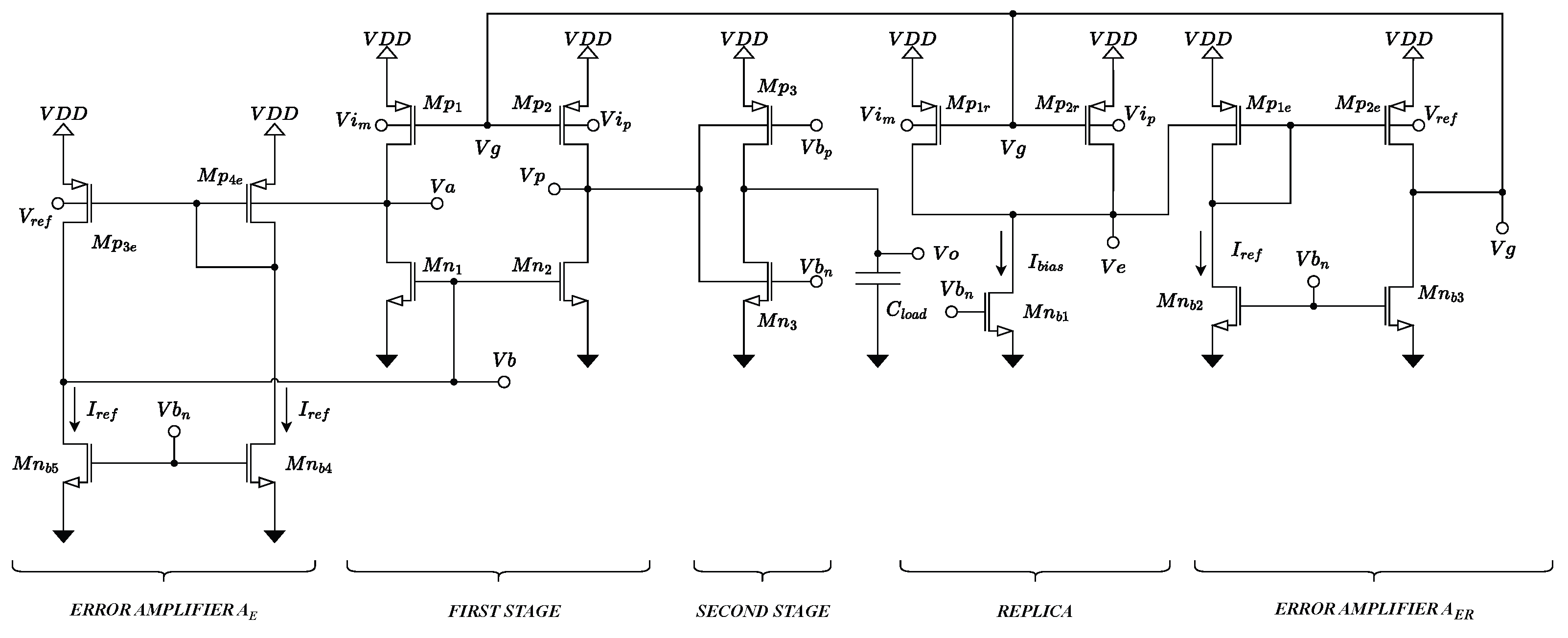
The proposed amplifier features a standard two-stage architecture, as shown in
Figure 1; body-driving is exploited in both stages to allow for a rail-to-rail input common-mode range (ICMR) and keep gate terminals available for robust biasing. Both NMOS and PMOS body terminals are exploited as inputs of the second stage to enhance gain.
With reference to
Figure 1, the input stage is composed of transistors
and
. The input is applied to the body terminals of the PMOS devices, whose gate terminal is exploited to set the bias point. NMOS devices are used to form a current mirror load. To improve CMRR, the NMOS current mirror is enhanced through the use of an auxiliary amplifier
that helps with reducing gain error. A simple single-stage body-driven auxiliary amplifier is used; it exploits a reference voltage
that helps with achieving a robust bias point.
The first stage of the OTA is critical in achieving robust bias and high CMRR. To improve performance, the bias point is set through the use of a replica bias stage (
in
Figure 1). The input signal is applied to the body terminals of the replica bias stage, whose role is to keep the bias current constant at
, counteracting the variations of PVT and of the input common-mode voltage. Additionally, an auxiliary amplifier is exploited to improve the diode connection of
, and it is designed identically to the auxiliary amplifier of the input stage. The voltage reference applied to the amplifier keeps the drains of
at the desired voltage (typically
), equal to the drain voltage of
, controlled by the auxiliary amplifier of the input stage (the same reference
is applied to both amplifiers). The replica bias stage thus implements common-mode feedforward (CMFF) to improve CMRR and yields a robust bias point against PVT variations.
It has to be noted that the proposed approach, based on the use of auxiliary amplifiers with an explicit reference voltage, enables setting the gate-source voltages of the transistors independently from their drain-source voltages; hence, the operating point of the transistors can be optimized while still keeping their drain-source voltages at . Moreover, this approach can also be applied in simple p-well CMOS technologies that do not allow isolated wells for NMOS devices.
With reference to a more common triple-well technology, a simple body-driven inverter is exploited as the second stage, and its bias point is set through the gate terminals. Bias voltages
and
in
Figure 1 are generated through current mirror connections (diode-connected devices driven by current sources) in order to retain the current constant notwithstanding PVT variations.
2.2. Analysis of Biasing Approach
A replica-bias approach is exploited to precisely set the bias current of the first stage of the OTA, making it independent on PVT and input common-mode variation. With reference to
Figure 1, the replica bias stage, composed of
, the current source
, and the auxiliary amplifier
, is used to set the bias current of
to
, where
K is the ratio of the form factors of devices in the main and replica stages.
Recall that the drain current of an MOS device operating in sub-threshold is given by
where
and
are gate-source and drain-source voltages;
is the threshold voltage and depends on the body-source voltage
(body-effect) and on
(DIBL, drain-induced barrier lowering);
is the thermal voltage,
n is the subthreshold slope. Recall as well that the current
is given by
where
is the mobility of electrons (holes),
is the oxide capacitance per unit area, and
W and
L are the width and length of the gate, respectively.
The replica bias loop adjusts the gate voltage of
so as to keep the sum of their currents equal to
, contrasting PVT variations. that affect
and
in (
1), and variations of the input common-mode voltage, that changes
. The same gate voltage is applied to the gates of
, thus controlling their current. Instead of a simple diode connection, a feedback loop involving the auxiliary amplifier
is exploited in the replica stage. This approach not only improves the precision of the replica stage, but also enables keeping the drain-source voltages of
constant and equal to
, within the limits of finite loop gain. This results in better matching of devices in the main and replica stages, and hence, a more robust biasing.
The replica bias loop is schematized in
Figure 2, where
represents the variation of the current of
with respect to its nominal value,
is the small-signal component of the reference current (we are assuming an ideal current source
),
is the small-signal component of the reference voltage, and
is the voltage gain of the auxiliary amplifier:
where
is its output conductance, and
is the impedance at the output of the replica stage:
In the previous equations, standard nomenclature is used for the small-signal parameters of the MOS devices. Subscript r refers to . Subscripts and refer to the PMOS and NMOS devices af the auxiliary error amplifier, and is the output conductance of the current source in the replica stage.
The scheme in
Figure 2 enables calculation of the residual current error of the replica stage
as
The same error is achieved in the main stage, in the limit of matched drain-source voltages.
Looking at the main amplifier, the voltage generated by the replica loop is applied to the gate terminals of the input devices . The enhanced current mirror load exploits an auxiliary amplifier that sets the drain voltage of (and, by symmetry, of ) to , within the limit of its finite loop gain. The input devices thus present the same gate-source, drain-source, and body-source voltages as their replica counterparts, resulting in robust biasing.
This approach mimics the behavior of a tailed differential pair: within the limit that the replica stage correctly estimates the common-mode current, when a differential input signal is applied, the replica loop keeps the sum of the drain currents of and constant, thus transforming the input stage into a truly differential stage.
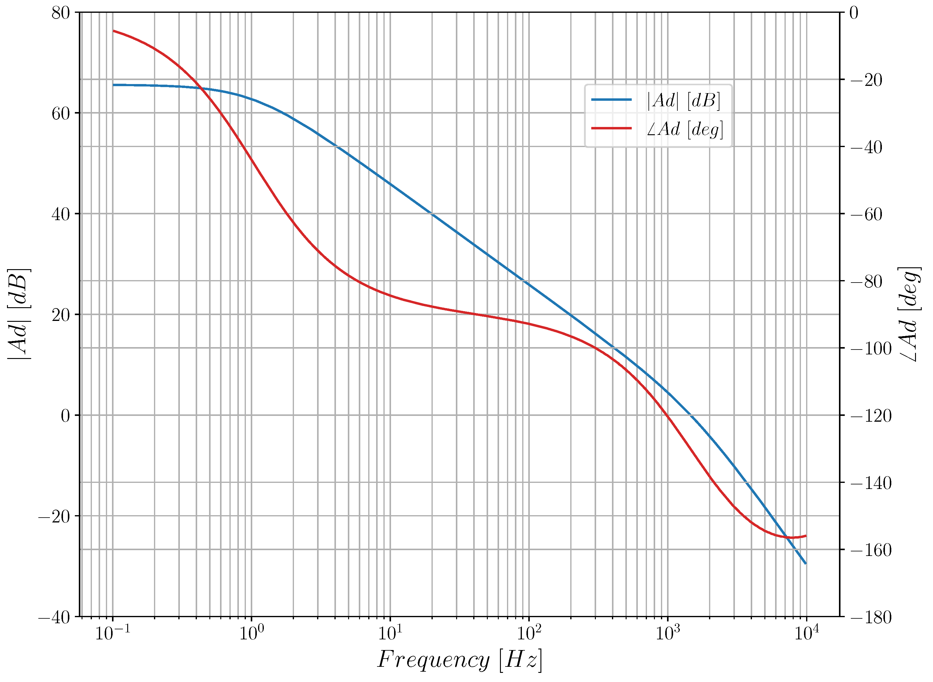
2.3. Differential-Mode Analysis
To analyze the small-signal behavior of the proposed amplifier, we can refer to
Figure 3, where the capacitances at the different nodes have been explicitly shown.
where
and
are the input and output capacitances of the auxiliary amplifier,
is the output conductance of the first stage, and
and
are transconductance and output conductance of the second stage. Standard nomenclature is used for the small-signal parameters of the MOS devices. Subscript
p refers to
, subscript
n refers to
, and subscripts
and
refer to NMOS and PMOS devices of the second stage. The same auxiliary amplifier as in the replica stage has been used; hence,
is given by (
3) (we are neglecting the pole-zero doublet due to the current mirror) and
Let us consider initially the differential-mode transfer function (
). The gate terminals of
can be assumed at virtual ground; hence,
. From
Figure 3, the transfer function of the first stage, exploiting the Miller approximation, can be obtained as
where the two pole-zero doublets due to the enhanced current mirror can be neglected, and the transfer function of the second stage is given by
The differential-mode gain is therefore
where the two poles are
For a sufficiently large load capacitance
, the dominant pole is given by
, and an adequate phase margin is achieved, otherwise some form of compensation is needed. Assuming to be in the large-capacitance case, the gain-bandwidth product (GBW) can be easily calculated as
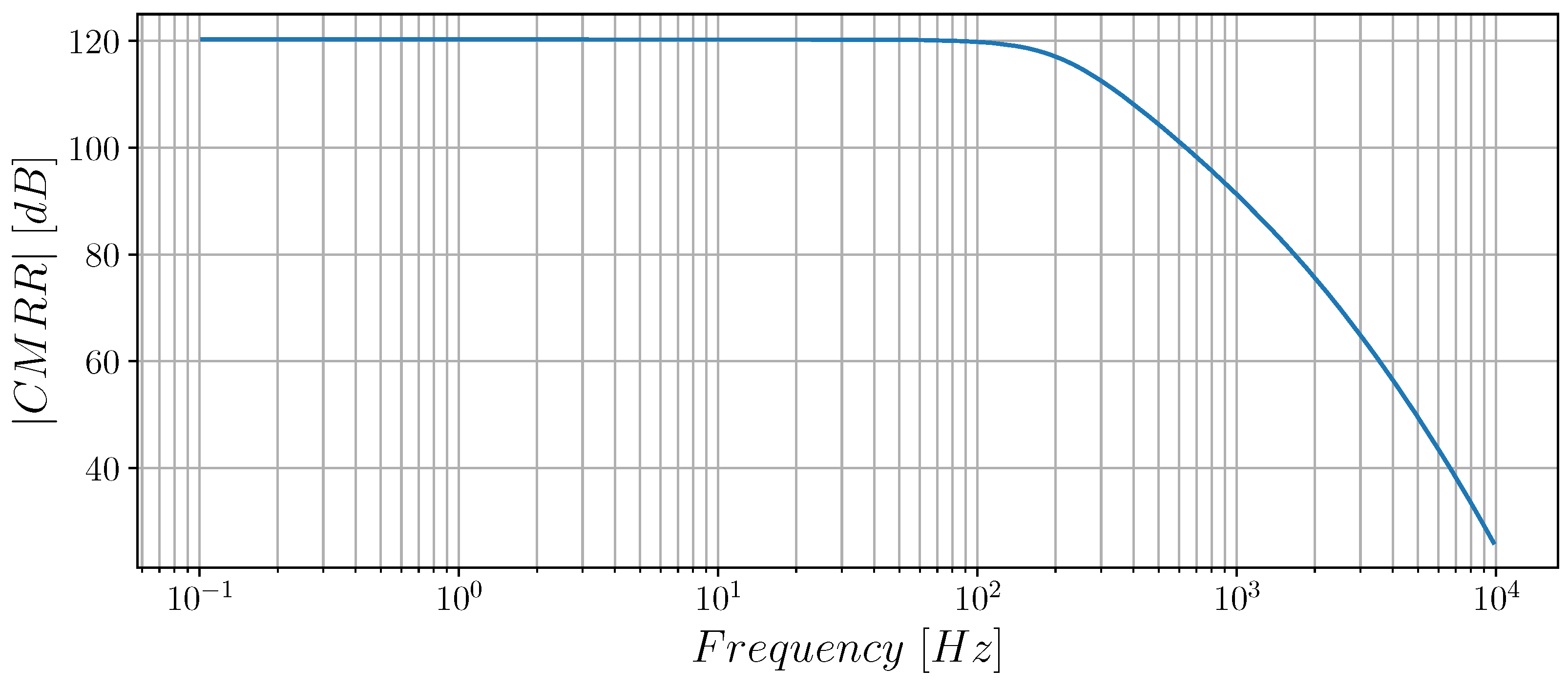
2.4. Common-Mode Analysis
The common-mode gain of the proposed amplifier is affected both by the enhanced current mirror used for differential to single-ended conversion and by the replica loop. To separately analyze these two effects, we can start analyzing the scheme in
Figure 3 in the case of common-mode excitation (
) with
. The analysis yields the common-mode gain of the first stage as
Equation (
18) highlights the effect of the enhanced current mirror. We note that
is given by the differential mode gain (
12) times the reciprocal of the current gain error of the mirror. Using a simple current mirror (with gate and drain of
connected together), the current gain error is inversely proportional to gm/gds, whereas in this case the error is scaled down by the gain of the auxiliary amplifier
.
The replica bias loop keeps constant the sum of the drain currents of
, counteracting the effect of the input common-mode signal. Hence, voltage
depends on the input common-mode signal
, and the overall common-mode transconductance gain of the pair
results lower than the value of
used in (
18). The effect is similar to a tailed differential pair, where the common-mode input signal sees a source degeneration that reduces the transconductance.
The block scheme in
Figure 2 can be used to calculate
as a function of
, observing that current
in
Figure 2 is given by
. A simple analysis yields
The common-mode transconductance of
therefore becomes
and this is the correct value to be used in (
18). The overall common-mode gain of the amplifier is thus given by
and CMRR results as
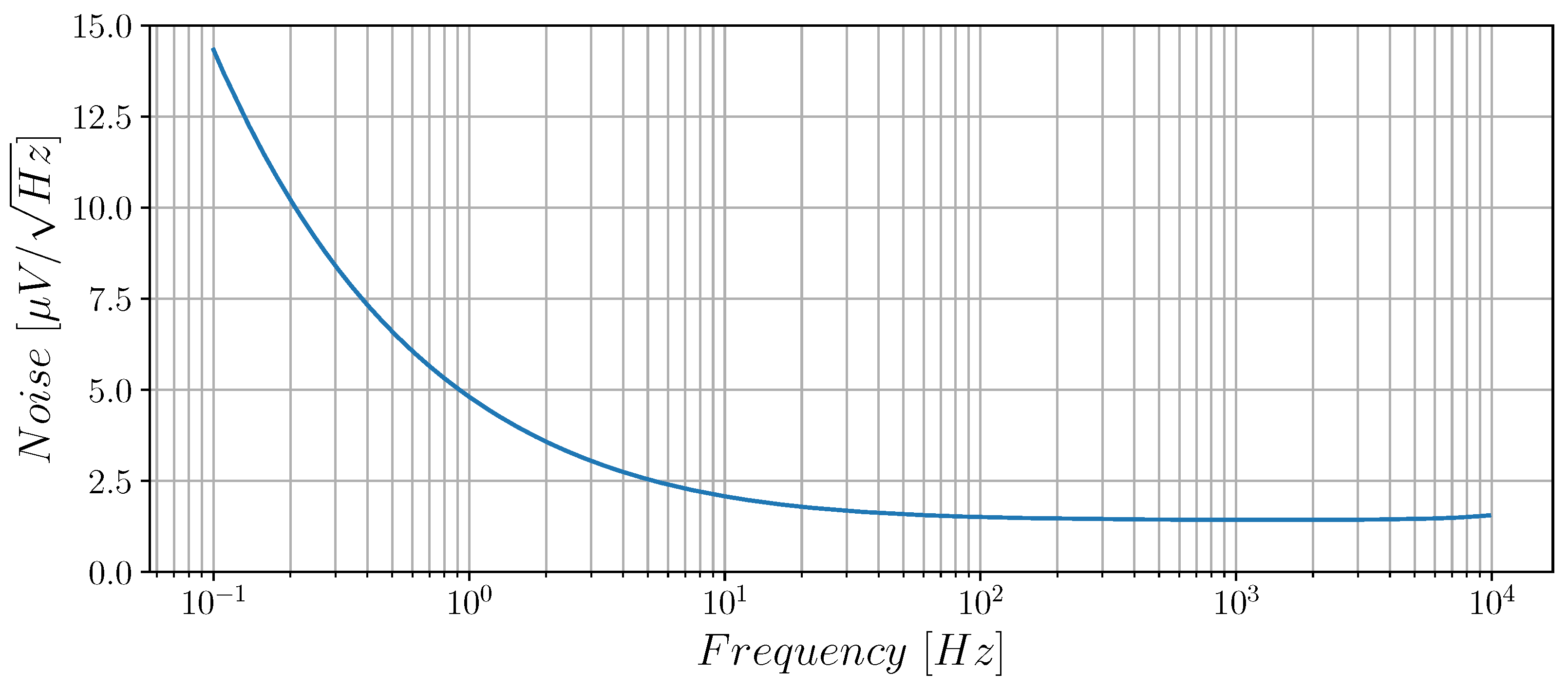
2.5. Noise Analysis
To analyze the noise performance of the proposed OTA, we consider for each transistor
in
Figure 1 a noise current source
that includes a thermal noise component with spectral density
(where
is the bias current of the device) and a flicker noise component with spectral density
We calculate the open-circuit output voltage due to the different noise sources, and dividing it by the differential gain (
14), we obtain the equivalent input-referred noise voltage.
Noise sources of transistors of the second stage (
and
) are directly connected to the output and yield an output voltage
Neglecting the gain error of the current mirror, the noise sources of the main devices of the first stage (
and
) yield an output voltage
that is the main noise contribution of the OTA. Noise sources in the auxiliary amplifier (devices
and
) yield a common-mode contribution that is attenuated by the CMRR. Noise in the replica stage appears at the gates of
and is amplified by the common-mode gain (
21), resulting in a very small contribution that can be neglected.
As a result, the equivalent input noise spectrum is given by
and by using (
23) and (
24), it can be written as
where
,
, and
are the bias currents of devices in the first stage, in the second stage, and in the auxiliary amplifier, respectively.


