1. Introduction
As artificial intelligence (AI) technologies have recently generated considerable research interest, technological advancements for handling large amounts of data are increasingly necessary [
1,
2,
3]. In an era of big data, conventional computational systems based on von Neumann architecture are limited in their ability to efficiently transfer data between memory and computing units due to a bottleneck [
4]. In recent decades, remarkable progress in neuro-inspired computing has been made to achieve a human brain-like performance by using electronic devices that can implement adaptive parallel processing [
1]. Such systems have been executed in the field of hardware neural networks (HW-NNs), which consist of numerous artificial synapses that perform cognitive and computational capabilities. Numerous experiments have successfully emulated several characteristics of biological synapses, such as updating or memorizing the conductance of electronic devices (called a synaptic weight) using an external voltage or an optical stimulus [
5,
6]. One of the most promising hardware platforms used for the implementation of an artificial synapse is emerging non-volatile memory (eNVM) devices, which have extremely compact designs using a two-terminal structure. eNVM categories include resistive random-access memory (RRAM) [
7], ferromagnetic random-access memory, (FeRAM) [
8], and phase change random-access memory (PCRAM) [
9], according to the physical mechanism used in each. Despite the progress that has been made in eNVM devices, there are still many challenges to overcome before they can achieve the same level of accuracy as the biological brain and software neural networks [
2]. These challenges arise from eNVM operations that do not sufficiently satisfy the required synaptic characteristics, such as a linear/symmetrical conductance change, device-to-device variation, dynamic range, and the number of conductance states.
Among the various eNVMs, Ge
2Sb
2Te
5 (GST225), one of the representative materials of PCRAM, is a two-terminal device that has been heavily researched in regard to synaptic device applications [
10]. It operates by differentiating the resistance between the crystalline state of the phase change material with high electrical conductivity, and the metastable amorphous states with low electrical conductivity. Switching is generally performed by Joule heating the amorphous material to above the crystalline temperature of 150 °C to create the conductive state. Conversely, the highly resistive amorphous state is achieved by melting the crystalline material above 625 °C, followed by quenching [
11]. Based on this melting-quenching mechanism, the change in analog conductance for neuro-inspired computing in phase change materials can be classified according to the volume ratio of the crystalline and amorphous states [
2,
9]. Due to these characteristics, GST225 is well known to have advantages in terms of scalability, reliability, and multi-level resistance programming. However, operating GST225 with Joule heating consumes considerable amounts of energy, as rapid, high-current pulses must be applied to achieve the amorphous state [
11]. In addition, it is difficult to precisely control the phase change volume to implement gradual conductance state changes and long-term potentiation (LTP) and long-term depression (LTD), which are used to emulate synaptic weight [
9]. Although this issue can be overcome with the use of 2-PCM architecture and peripheral circuit design, there are still limitations with respect to complex device operation and scalability [
12].
To address these issues, interfacial phase change memory (iPCM), based on van der Waals heterostructures, has been developed by alternately depositing ultra-thin films of (GeTe/Sb
2Te
3)
n, where
n is the number of stacked layers, as proposed by Tominaga et al. [
13]. The iPCM superlattice structure is designed such that the Ge atoms in the GeTe layers undergo vertical and lateral displacement at the thin-film surface. Although the specific mechanism of the iPCM operation has not been definitively established, it is clear that when an external voltage is applied to the iPCM, the Ge atoms play a key role by changing the bonding structure between high-resistance covalent bonding and low-resistance resonant bonding [
14,
15]. Therefore, the iPCM reduces the total entropy by limiting the movement of Ge atoms by establishing a vdW gap between the thin films [
13]. This process enables the iPCM to consume less energy than GST225 and achieve faster device operation. Furthermore, it is highly probable that iPCMs provide more sophisticated changes in resistance by restraining atomic movement, which maintains the crystalline state. However, there remains a need to effectively demonstrate the synaptic properties exploited in neuro-inspired computing by changing the conductance values.
In this study, to understand the application of HW-NNs, we fabricated sputter-grown iPCMs based on the GeTe/Sb2Te3 superlattice structure. We further examined the dependence of conductance on the voltage-based electrical pulse width by analyzing the bidirectionality of the (GeTe/Sb2Te3)16 iPCM by applying incremental step pulse programming (ISPP). Based on this relationship, an optimized sequence of identical fast pulses was designed and applied to the (GeTe/Sb2Te3)16 iPCM to implement both linear and gradual conductance modulation. We present the possibility of utilizing artificial synapses through a newly designed iPCM device with a superlattice structure.
3. Results and Discussion
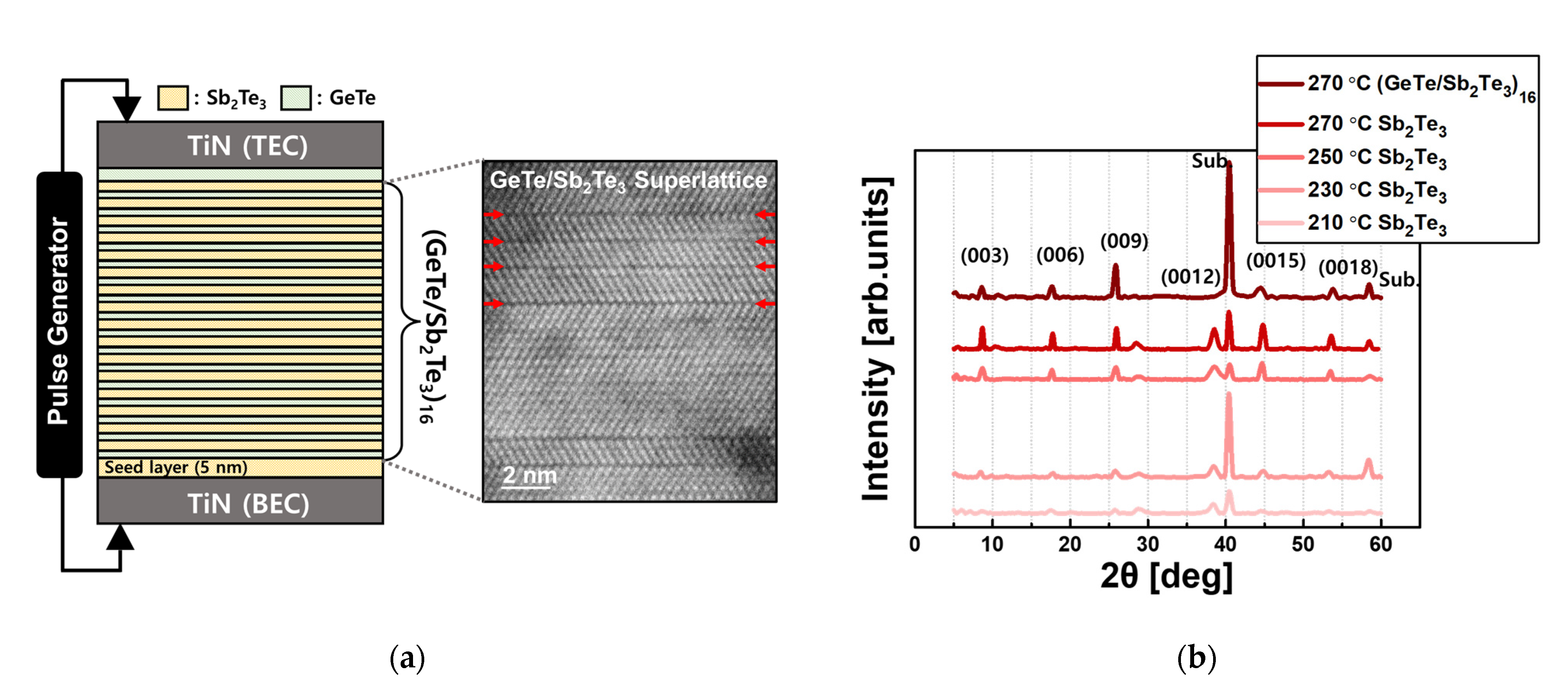
The XRD spectra of bulk Sb
2Te
3 and (GeTe/Sb
2Te
3)
16 iPCMs with growth temperatures ranging from 210 °C to 270 °C are shown
Figure 1b. All observed peaks can be indexed as (00
l) peaks of the Sb
2Te
3, indicating that the fabricated samples possess the preferred orientation: with the c-axis perpendicular to the substrate surface. Increases in the annealing temperature correspond to crystal growth along the (00
l) orientation.
Figure 1b clearly shows that the most highly oriented Sb
2Te
3 film was grown at 270 °C. This result suggests that the thin film with the best quality under different growth conditions can provide a seed layer for the two-step growth method. Therefore, the (GeTe/Sb
2Te
3)
16 iPCM deposited at an annealing temperature of 270 °C grew to be highly oriented. However, no peaks that originated from the GeTe were observed, which indicates that the Ge atoms are in different positions when compared to the orientation of the substrate. In addition, it can be seen that the full width at half maximum (FWHM) of the peaks in the (00
l) direction are broadened in the (GeTe/Sb
2Te
3)
16 structure. There is a strong possibility that this broadening is caused by Sb
2Te
3 strain due to the Ge atoms moving or intermixing between layers [
16].
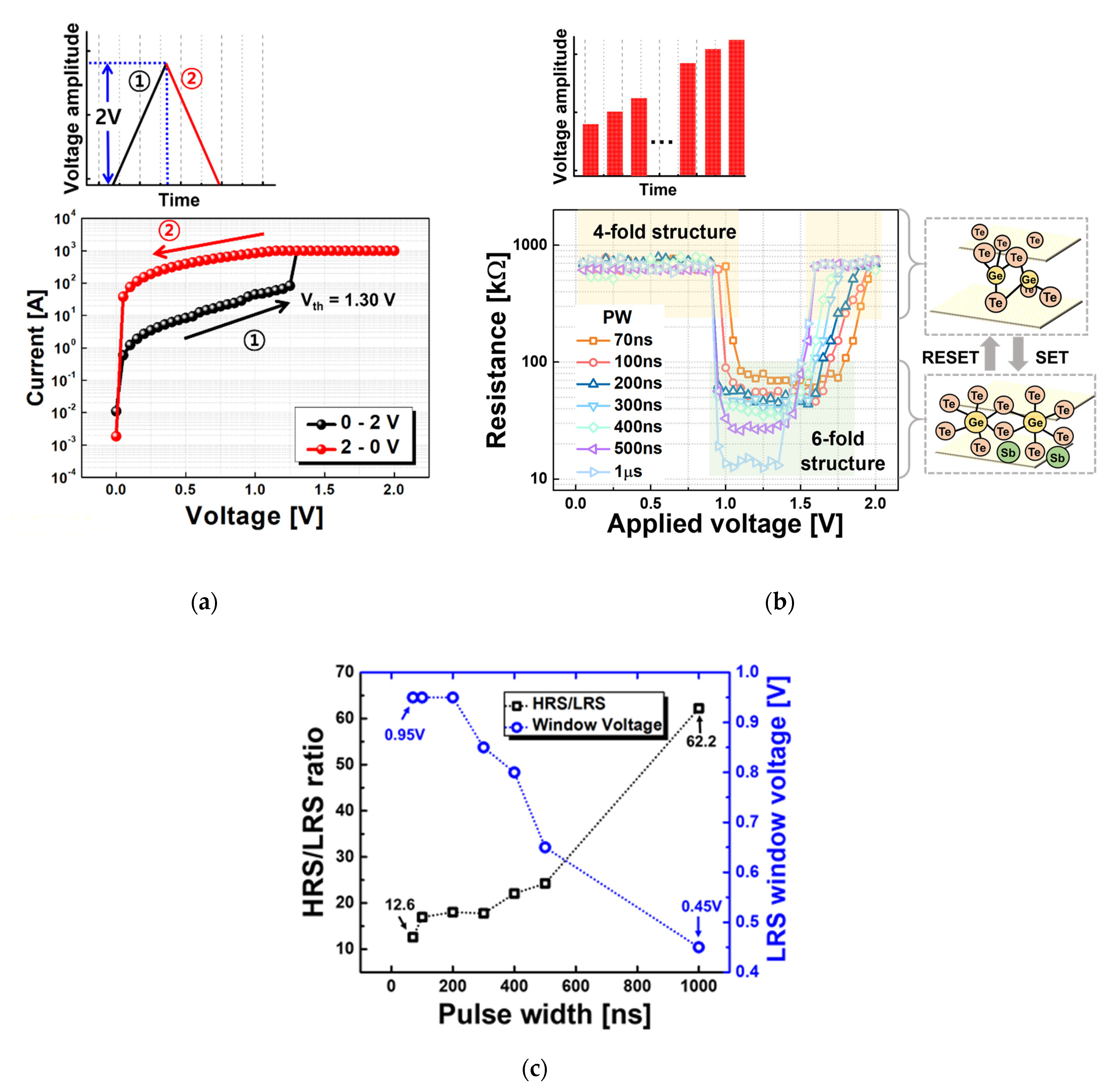
The main goal of the experiment is to demonstrate the potential switching nature of the synaptic characteristics of the iPCM. To check the initial condition of the memory characteristics, the DC regime of the (GeTe/Sb
2Te
3)
16 iPCM was performed, as shown in
Figure 2a. The applied voltage was designed to gradually increase from 0 V to 2 V and then return to 0 V. During the first process, the resistance decreases at 1.3 V (RESET to SET transition), and in the second, the resistance was maintained, showing the unipolar switching behavior. It should be noted that GeTe/Sb
2Te
3 does not function as an ovonic threshold, but as a memory device. The resistance–voltage (R-V) curves in the (GeTe/Sb
2Te
3)
16 iPCM memory cell are shown in
Figure 2b. The pulse programming consists of 0.05 V rectangular pulses applied to the (GeTe/Sb
2Te
3)
16 iPCM with a given pulse width (PW). Bidirectional switching was observed, in which both the high-resistance state (HRS) and the low-resistance state (LRS) coexisted at one polarity under all ISPP conditions (fixed at 70 ns–1 μs). We generally refer to the transition from the HRS to the LRS as the SET operation, and the opposite is called the RESET operation. The iPCM mechanism is strongly influenced by the bonding phase of Ge atoms, as mentioned earlier. Covalently bonded Ge atoms in the superlattice-structured iPCM are separated by a crystalline Sb
2Te
3 plane. As shown in the simplified model in
Figure 2b, the distributed Ge atoms in the GeTe layer are switched from a covalently bonded four-fold structure to a resonantly bonded six-fold structure by a charge injection. DFT calculations confirmed that the four-fold structure and the six-fold structure were both stable [
17,
18].
Figure 2c shows that as the PW applied to (GeTe/Sb
2Te
3)
16 iPCM increased, the resistance ratio between HRS and LRS increased, and the window voltage that maintains the LRS decreased. Moreover, the threshold voltage for transitioning from the initial RESET state to the SET state was 0.1 V higher at 70 ns PW than at 1 μs PW. In the case of ISPP with a PW of 1 μs, the resistance ratio, which is the highest HRS value divided by the lowest LRS value, was about 62.2, and the LRS window margin was 0.45 V, as shown in
Figure 2c. On the other hand, when ISPP was applied with the shortest PW of 70 ns, a resistance ratio of about 12.6 and a SET margin of 0.95 V was obtained. This result seems to imply that a trade-off exists between the resistance ratio and the window margin of the LRS.
Interestingly, the R-V characteristics were not as clearly controlled by PW for GST225 alloy as they were for (GeTe/Sb
2Te
3)
16 iPCMs. This difference is due to the less-ordered GST225 alloy having a broad distribution of transition energies, as atomic movement occurs in all directions. Therefore, it is difficult to perform a stable operation using PW in the GST225 alloy when compared to the ideal order of the Ge atoms of the GeTe interface. Moreover, a (GeTe/Sb
2Te
3)
16 iPCM can be expected to lower the operating voltage due to the entropy reduction from the limited atomic movement of Ge atoms located between the Sb
2Te
3 layers, which is a hexagonal template in an ideal superlattice nature. In the ideal case, the Ge atoms experience the same force and change from resonant bonding with low resistance to covalent bonding with high resistance when an electric pulse is applied to the GeTe thin film in the iPCM nanostructure. However, an actual (GeTe/Sb
2Te
3)
16 iPCM has different switching characteristics depending on the PW condition because the vdW interaction does not apply the same force to all layers and the Ge atoms in the GeTe thin film are not all located at the interface, which is discussed in more detail below. Note that, as shown in
Figure 2a, when the PW is applied to the shortened ISPP, (GeTe/Sb
2Te
3)
16 iPCMs have the potential for more intermediate states to emerge. This result implies that the (GeTe/Sb
2Te
3)
16 iPCM has the latent ability to implement gradual LTP/LTD, which is one of the synaptic properties that is suitable for analog design, according to the appropriate electrical pulse programming.
To implement an artificial synaptic device using the iPCM, gradual and symmetric LTP/LTD and multiple conductance values that mimic analog behavior should be achieved by applying electrical pulses. The application of identical pulses of equal intensity places less burden on the circuit than more complex programming schemes, such as varying the voltage amplitude or the pulse width.
Figure 3 displays the conductance-voltage (C-V) graph when applying the (GeTe/Sb
2Te
3)
16 iPCM according to the PW and voltage amplitude in the identical scheme. The solid lines in the graph correspond to the Boltzmann functions along the conductance values to clearly compare linearity. An identical pulse scheme with an amplitude of 0.6 V exhibits potentiation properties that increase the conductance values, as shown in
Figure 3a. To initialize the first (GeTe/Sb
2Te
3)
16 iPCM with high resistance, ISPP with 1 μs PW was applied to achieve the HRS. As the PW of the pulse scheme increased, the conductance also increased. Each PW of a given pulse scheme produced a different maximum conductance value at saturation. When comparing the 70 ns PW to the 1 μs PW, it appears that the conductance of the 70 ns PW gradually increased and has more effective conductance states. This characteristic is consistent with the bidirectional switching properties shown above. Therefore, it can be inferred that there is a trade-off between the dynamic range and the effective conductance states, as determined by PW. In addition, this result implies that identical pulse schemes with PW modulation can be used to implement multiple values of conductance or potentiation.
Figure 3b shows the conductance values produced by the application of a given pulse scheme with the PW fixed at 70 ns and at different voltage amplitudes (1.6 V to 2.2 V) to the (GeTe/Sb
2Te
3)
16 iPCM. When the amplitude is greater than 1.6 V, the pulses have the characteristic of a depression, in which conductance decreases. Initialization was set by applying an identical 0.6 V pulse scheme with a 70 ns PW until saturation. It was observed that the effective conductance states were not sufficiently implemented in the identical pulse scheme with a voltage amplitude of 2.2 V because the conductance values fell abruptly at this voltage. In the case of the identical pulse scheme at 1.4 V, the conductance decreases too gradually, making it difficult to distinguish the varying conductance values. Therefore, considering the possible conductance states and the dynamic range, it is reasonable to suppose that the identical pulse scheme with an amplitude of 1.8 V is suitable for a depression pulse. The evidence suggests that if voltage amplitude and conductance values are precisely controlled, not only does conductance increase or decrease gradually but a high symmetry between potentiation and depression can also be realized.
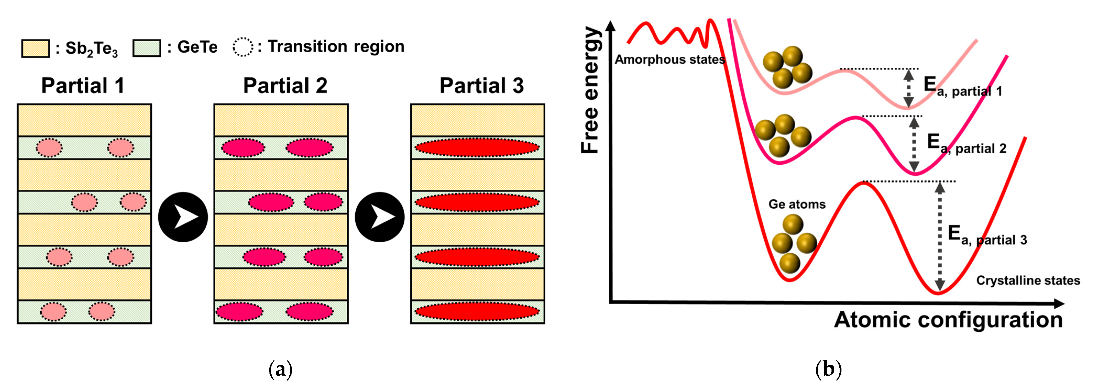
As illustrated by
Figure 4a, we modeled the GeTe/Sb
2Te
3 iPCM to discuss how it can implement multiple conductance states. When the phase transition in the superlattice structure is considered as an equivalent circuit model, it can be viewed as a partial or parallel model. In the parallel model, the GeTe layers shift one by one, and in the series structure, the phase transition partially occurs in the entire layer. Since more conductance states are found than the number of GeTe layers, it seems that the GeTe/Sb
2Te
3 iPCM is better described by the partial structure model rather than by a parallel structure. This result is consistent with those for devices with TiTe
2/Sb
2Te
3 superlattice structures [
19]. Furthermore, the partial transition region restricts structural relaxation by the nanosized effect. It can be assumed that this effect can prevent the conductance variation that is critical to the synapse operation that occurs in GST225 alloy. Indeed, the Te-Te antibonding interaction between the thin films and the Sb
2Te
3 bonding pairs interfere with the enhancement of the Peierls distortion [
20]. Therefore, as shown in partial model 1 of
Figure 4a, an identical pulse scheme with short PW or low voltage amplitude is proportional to the amount of energy applied to the iPCM, implying a relatively small area of transition.
As the PW, voltage amplitude or the number of applied pulses increases, the partial area becomes wider and saturated due to an avalanche of Ge atomic switching caused by biaxial strain [
21]. This result is reasonable, as studies have shown a temperature distribution resulting from the application of an external stimulus to a superlattice device.
Figure 4b schematically describes the interatomic potential for Ge atomic switching for partial 1, 2 and 3. In partial 1, Ge atoms are in a region that requires a low activation energy for diffusive atomic switching, which could be represented by a short PW. In this situation, more Ge atoms must cross a larger energy barrier to flip through the Te plane. Therefore, it can be inferred that the switching process of the iPCM has a linear dependence with multiple conductance states. It can be inferred that partial 1 can be controlled more precisely when a short PW is applied. Evolution from partial 1 to either partial 2 or straight to partial 3 occurs when a continuous pulse train is applied to partial 1. On the other hand, there is a strong possibility that partial 1 and 2 will be skipped, and that a sharp transition will occur when sufficient activation energy is applied to cross the energy barrier. However, in actual Ge atomic movement near the vdW gap, there is an additional lateral process or a complex switching process that includes intermixing with the Sb
2Te
3 layer.
On the basis of the observed analog behavior driven by the iPCM systems, we evaluated the synaptic weight cumulative characteristics by applying optimized pulses, as shown in
Figure 5. In addition, when comparing
Figure 5a–d shows the disparity in the characteristics of artificial synapses that employ GST225 alloy and (GeTe/Sb
2Te
3)
16 iPCM.
Figure 5a illustrates a pulse programming design that differentiates between potentiation pulses and depression pulses for GST225 alloy using the melt-quenching mechanism. The application of this pulse scheme results in appropriate electrical excitation to control the amorphous and crystalline states in the active region. For potentiation, a pulse scheme decreasing by 0.05 V steps from 2 V to 0.5 V and using 3 μs PWs was applied for Joule annealing. In contrast, the depression pulse scheme increased from 2.5 V to 4 V using 70 ns PWs to accomplish the melting of materials in the crystalline state. As shown in
Figure 5a, gradual potentiation and depression with 30 conductance states were realized in the GST225 alloy by applying staircase pulses. However, it is well known that mushroom-shaped PCRAM devices usually abruptly change resistance to achieve amorphization and crystallization. The GST225 alloy samples also resulted in undesirable weight-update asymmetry in synaptic potentiation and depression (marked with a brown circle drawn in
Figure 5a). In the case of the (GeTe/Sb
2Te
3)
16 iPCM, the most gradual synaptic weight cumulative condition was implemented. It is reasonable to suppose that the voltage amplitudes for the depression pulse and the potentiation pulse should be 0.6 V and 1.8 V, respectively. Although the appropriate voltage amplitude could be changed by varying the PW, the synaptic characteristic can also be implemented by fixing the pulse width. As can be observed in
Figure 5b–d, all PW conditions (70 ns, 300 ns, 1μs) achieved potentiation and depression by applying the identical pulse scheme.
To compare synaptic characteristics, the nonlinearity (NL) of the GST225 alloy and the (GeTe/Sb
2Te
3)
16 iPCM were calculated for the applied pulse programming schemes. NL was adopted to effectively analyze the LTP and LTD phenomena, which are characteristics of a bio-synapse. The calculation was derived using Equation (1).
GP (
n) and
GD (
n) are the conductance values after the nth potentiation pulse and depression pulse, and
N is the number of potentiation pulses/depression pulses.
Table 1 shows the results of the NL values calculated using Equation (1). The GST225 alloy showed a relatively large NL value of 0.58 due to the abrupt change in conductance during the phase transition between the amorphous and crystalline states. In the case of the (GeTe/Sb
2Te
3)
16 iPCM, as the PW shortened from 1 μs to 70 ns, lower values of NL were calculated. This result implies that the application of sufficient energy helps to exceed the activation energy barrier for the transition of the Ge atom that is saturated under the relatively long PW condition of 1 μs, in accordance with the partial model mentioned above. Therefore, under the condition of the shortest PW of 70 ns, the conductance values of LTP and LTD were more precisely controlled, as indicated by an NL of 0.32. Furthermore, PW is also related to the number of conductance states of LTP/LTD. In the identical pulse scheme with 70 ns PWs, 80 conductance states are implemented, demonstrating sophisticated conductance modulation. In contrast, 300 ns and 1 μs PWs could not generate sufficient effective conductance states for operation as synaptic devices.
However, the dynamic range for measuring the ratio of the largest conductance values to the smallest conductance values is 13.1 with 70 ns PW, whereas GST225 has the largest observed dynamic range of 90.2. As shown in
Table 1, the potentiation pulse scheme using 0.6 V and 70 ns PWs and the depression pulse scheme using 1.8 V and 70 ns PWs achieved the lowest NL value of 0.32. In addition, the conductance states achieved with these schemes implemented superior synaptic characteristics to those of other conditions through 40 levels of potentiation and depression. Although the conductance ratio has a narrow range, it is shown that a (GeTe/Sb
2Te
3)
16 iPCM can achieve a linear and symmetric LTP/LTD in identical pulse systems.
As shown in
Table 2, when compared with other studies related to PCM devices, in the case of 2-PCM [
22], symmetric LTP and LTD conductance states can be implemented, but two devices are integrated per synapse. Therefore, because peripheral circuits and a refresh are required for operation, it consumes a lot of energy. In addition, in the case of the conventional 1-binary PCM [
23] and the narrow bottom electrode PCM (h-BEC PCM) [
24], the number of possible conductance states is small, otherwise the conductance states of LTP and LTD are not symmetrical. In addition, in devices with pulse width programming based on other PCMs [
25], only the RESET process can gradually increase the resistance. However, (GeTe/Sb
2Te
3)
16 iPCM demonstrate that the SET and RESET processes either increase or decrease gradually, appear to have symmetrically conductance states, and are highly advantageous in neuromorphic computing.


