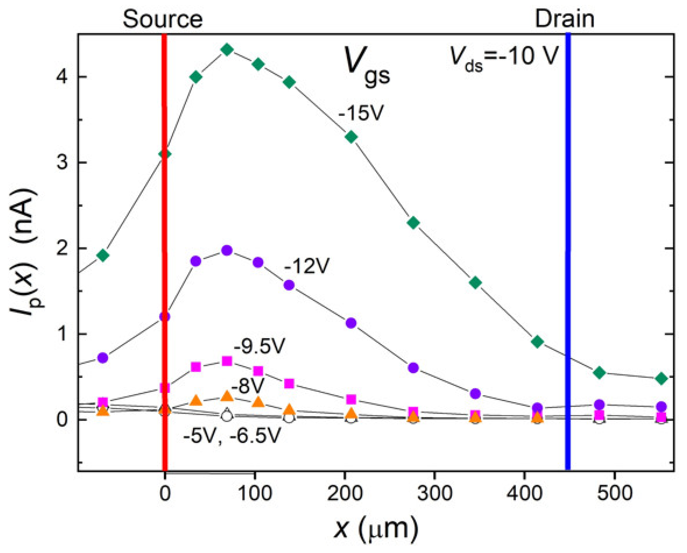
3.1. SPCM Profiles
The spatial photocurrent
Ip(
x) profiles, obtained by setting the chopper to the lowest frequency of
f = 10 Hz and scanning the laser beam along the transistor channel at different positions,
x, from the source edge, are shown in
Figure 1 for constant
VDS = −10 V and different negative
VGS ranging from −5 V to −15 V. For less-negative
VGS values down to −6.5 V, the
Ip(
x) signal in the channel is very low indicating that the transistor is in the off-state and the channel is depleted of charge carriers. By reducing the negative
VGS values to −8 V and −9.5 V, holes are accumulated at the pentacene insulator interface and the transistor switches to the on-state. During this transition, the
Ip(
x) signal on the source side increases showing a maximum at a distance
x = 70 μm from the source, whereas the
Ip(
x) signal on the drain side remains at nearly zero. For
VGS lower than −9.5 V, the maximum of the
Ip(
x) signal increases strongly, whereas the
Ip(
x) signal on the drain side starts to increase.
The behavior of the SPCM profiles in
Figure 1 can be rationalized by considering that local modulated laser excitation induces a modulated density
pac(x) per unit area of free holes (majority carriers) contributing to the signal
Ip(
x) according to [
6,
13]
where
μ(x) is the local intrinsic hole mobility and
E(
x) is the local lateral electric field along the channel. The modulated density
pac(x) of the holes is produced by the dissociation of the triplet excitons generated by the ultrafast singlet exciton fission process within the pentacene layer during each half-period of the chopped laser illumination [
17]. However, the triplet excitons dissociation into mobile holes is a low probability process that can be assisted by a high electric field. Such a high electric field may occur near the edges of the contacts due to a large voltage drop caused by significant contact resistance producing a local maximum photocurrent at the contacts [
9,
10,
11]. However, such a maximum in
Figure 1 is not observed at the source or drain contact edges, indicating low contact resistance. Therefore, all the applied
VDS voltage drops take place along the conducting channel of the transistor, which has the highest resistance due to the long channel length. An additional electric field perpendicular to the insulator interface is generated by the applied gate
VGS voltage. However, this field should be high enough to facilitate the exciton dissociation and this can occur for most negative
VGS gate-source voltages [
18].
Based on our previous analysis of the experimental results of SPCM in pentacene FETs [
13], the dissociation of the triplet excitons is mainly realized by the so-called hole-detrapping mechanism [
19]. According to this mechanism, triplet excitons diffusing in the pentacene layer can encounter trapped holes in the accumulation layer and interact with them. During this interaction, the electron of the triplet can recombine with the trapped hole. A hole is then released, increasing the density
pac(x) of detrapped holes contributing to the
Ip(
x) signal according to Equation (1). In this way, the inhomogeneous spatial profiles
Ip(
x) along the transistor channel of
Figure 1 mainly reflect an inhomogeneous density of detrapped holes
pac(x). This density in turn comes from the inhomogeneous pattern of the trapped-hole density
Nt(
x) along the pentacene–insulator interface due to inhomogeneous band bending.
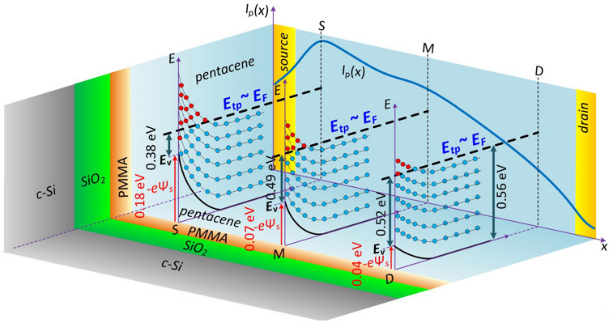
As the transistor is turned on for −9.5 V <
VGS < −6.5 V, the
Ip(
x) signal of
Figure 1 starts to increase only on the source side. This indicates that the negative gate voltage exceeds a threshold limit and the local negative gate potential
ΨS starts to increase creating upward band bending −
eΨS, shown schematically with the red upward arrows in
Figure 2. As the valence band of pentacene bends upward, deeper donor-like trap states (blue solid circles), which were initially in a neutral state and empty of holes below the
Etp level, are lifted above the
Etp level and become positively charged filled by trapped holes (red circles). These holes can be detrapped from the triplets when the laser beam probes the source side, producing the onset of an increase in the
Ip(
x) signal (
Figure 1). In contrast, near the drain the
Ip(
x) signal remains low, suggesting that there is no upward band bending because the negative gate voltage is canceled by the negative drain voltage
VDS = −10 V. By decreasing the
VGS beyond −9.5 V, the
Ip(
x) signal starts to increase on the drain side as well. This indicates that the negative effective gate voltage is not completely canceled out by the negative drain voltage and can now produce negative gate potential and upward band bending on the drain side as well. When the transistor is in the on-state, the
Ip(
x) profile shows a gradual decrease towards the drain, as in
Figure 1 and
Figure 3 with
VGS = −12, −15, and −20 V. This reflects a decrease in
Nt(
x) density and upward band bending due to the moderate and applied negative
VDS = −10 V, which provides that the transistor is operating in the saturation region for the above
VGS voltages, as confirmed from the output characteristics (not shown).
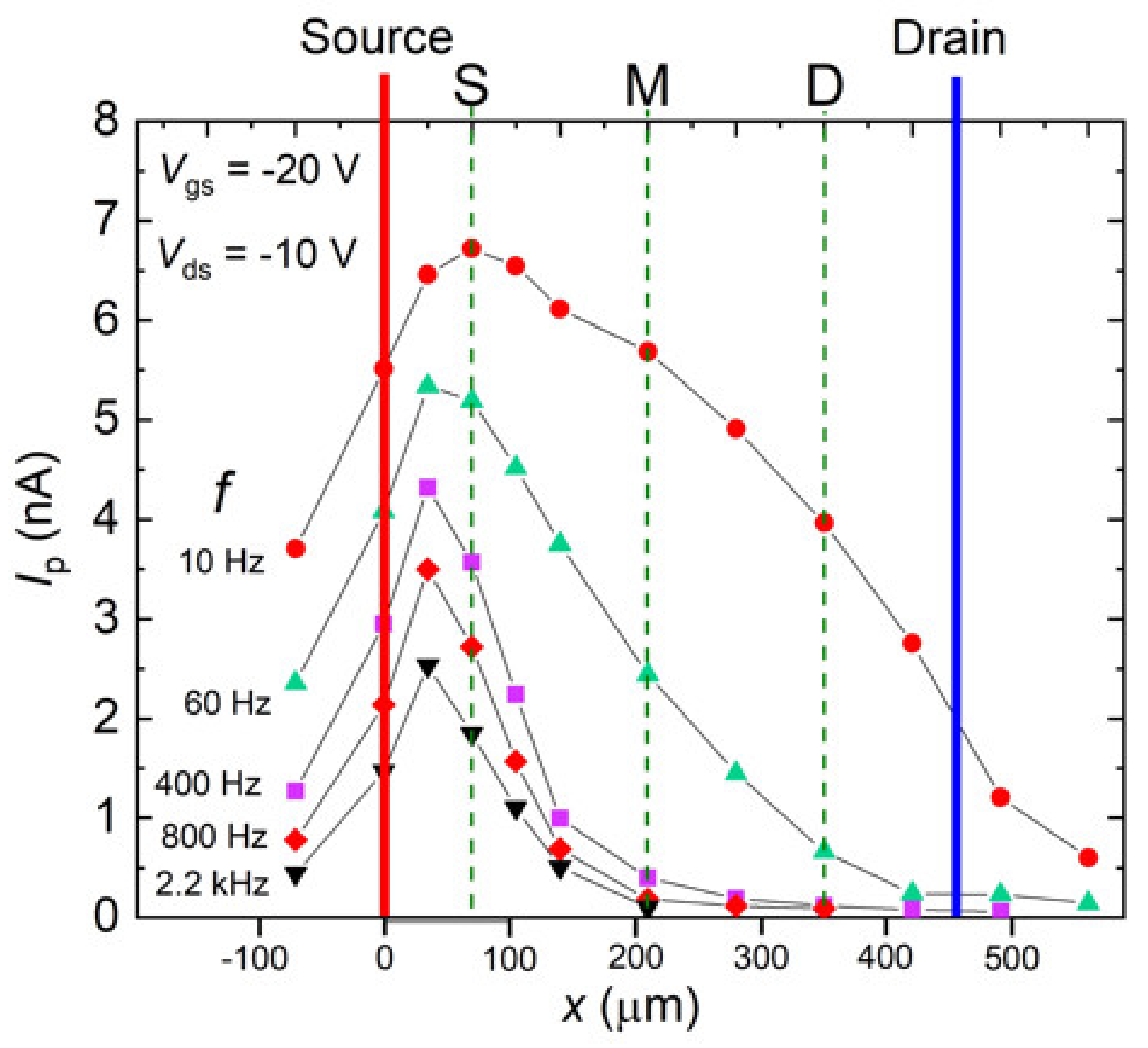
3.2. FR-SPCM Spectra
Figure 3 presents the
Ip(
x) profile of the photocurrent along the transistor channel obtained for different chopper frequencies
f ranging from 10 Hz to 2.2 kHz. The applied voltages were
VGS = −20 V and
VDS = −10 V, which set the transistor in the saturation region. It is obvious that the increase in the chopper frequency
f causes an overall reduction in the photocurrent
Ip(
x) in the whole channel. However, this reduction is relatively stronger on the drain side so that at the highest frequencies only the photocurrent near the source can be measured.
Westermeier et al. [
12] reported FR-SPCM measurements and found a decrease in the photocurrent with increasing frequency, which is similar to that found here in the
Ip(
x) profiles in
Figure 3. This dependence was attributed to trap-and-release events occurring at different time scales ranging from milliseconds to microseconds without specifying the energy level of the associated traps and their distribution [
12].
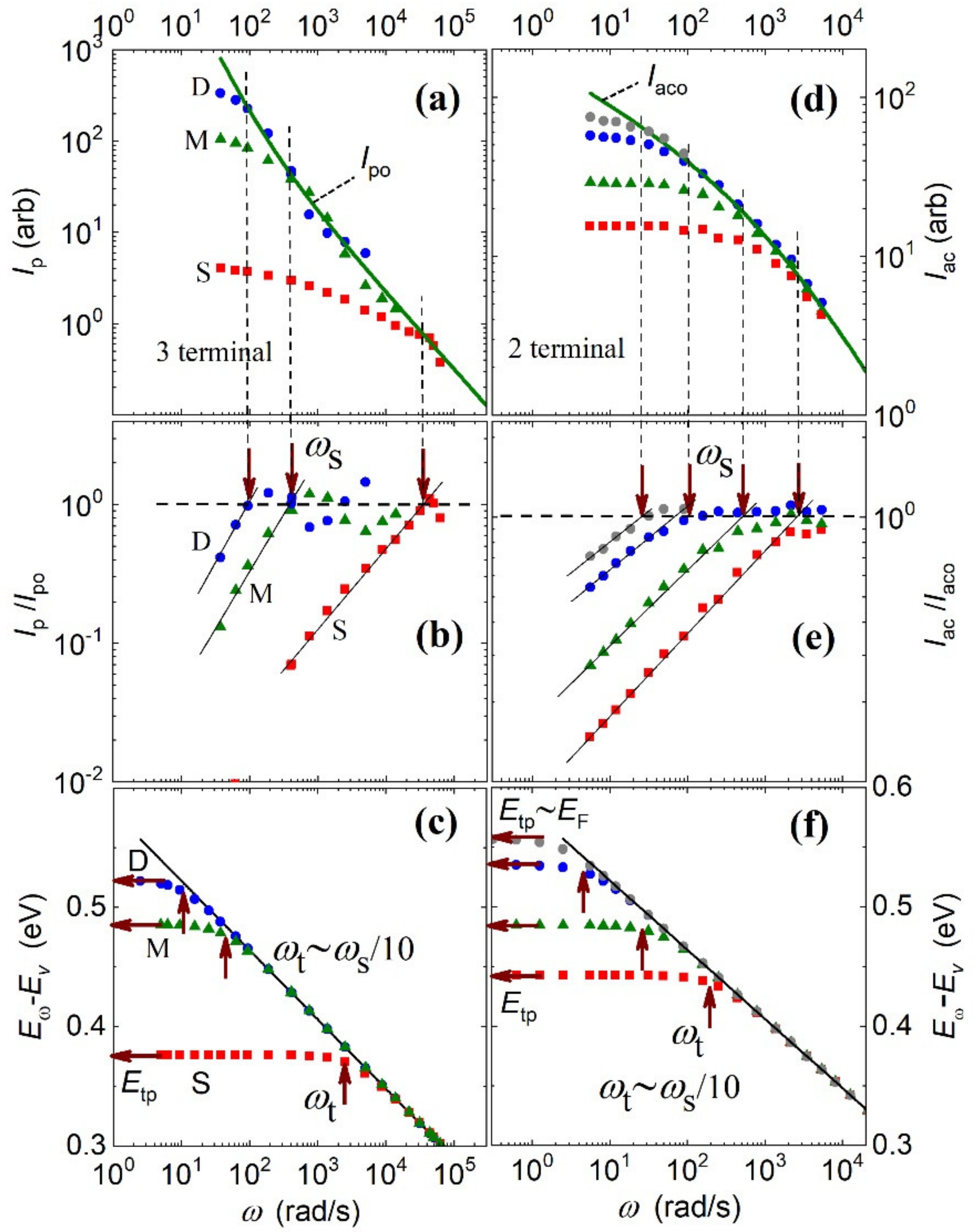
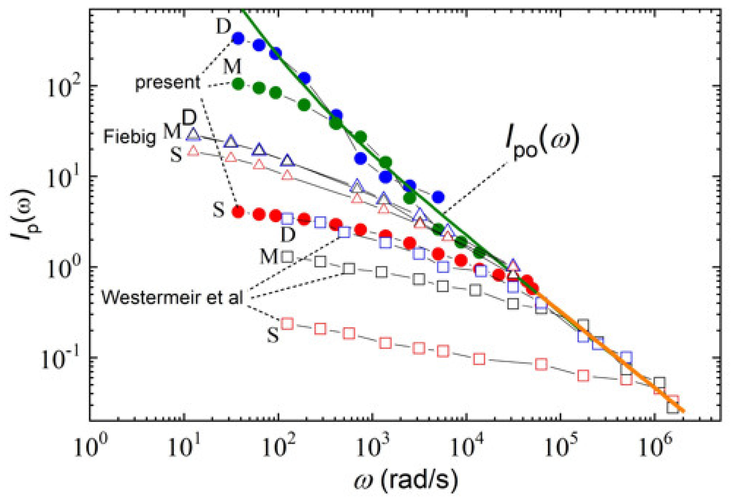
Here FR-SCPM measurements are employed to explore the microscopic processes responsible for the decrease in the photocurrent with frequency. For this purpose, the photocurrent was measured as a function of the angular modulation frequency
ω = 2 π
f by placing the probe laser beam at three different positions within the channel shown by the dashed vertical lines in
Figure 3. These lines, denoted as (S), (M), and (D), correspond to laser illumination near the source, midway between the source and drain, and near the drain, respectively. The
Ip(
ω) spectra of the different locations in the channel cannot be directly compared because the magnitude of
Ip(
x) is varied along the channel by the variations in the band bending. However, we found that if the
Ip(
ω) spectra are shifted vertically, they match each other at higher frequencies, as shown in
Figure 4a. In particular, the resulting
Ip(
ω) spectra of
Figure 4a after the appropriate vertical shifts, are merged at higher frequencies, defining the
Ipo(
ω) spectrum that has the form of an upper envelope (solid line) from all
Ip(
ω) spectra. The
Ipo(
ω) values of this envelope show a relatively strong decrease with increasing frequency, which is almost independent of the
x position of the probe illumination in the channel. Moreover, each
Ip(
ω) spectrum shows at a frequency
ωs (vertical dashed lines) a crossover from the strong frequency dependence at a higher
ω to a much weaker frequency dependence at a lower
ω. The crossover frequency
ωs is observed at a high, intermediate, and low frequency for the spectra with probe laser illumination on the source side (S), midway through the channel (M), and on the drain side (D), respectively. The above behavior of the
Ip(
ω) spectra resembles the corresponding behavior observed earlier in the photocurrent spectra of organic two-terminal devices [
15,
20], which are presented below for a detailed comparison with the present spectra.
3.3. Detailed Comparison with the Photocurrent Spectra of Two-Terminal Devices
The effect of light modulation frequency on the photocurrent has been previously studied in organic two-terminal devices on a glass substrate [
15,
20]. In these devices, the entire area of the organic semiconductor in the conducting channel, including the area of two parallel surface gold contacts, is uniformly illuminated by two beams of light from red light-emitted diodes with a maximum emission of 630 nm. One beam is called a probe light beam and its intensity is modulated by producing a modulated photocurrent (MPC) with amplitude
Iac, which is measured by a lock-in amplifier as a function of the angular modulation frequency
ω. The second light beam provides a constant-intensity continuous-wave (
cw) bias illumination called a bias beam. A typical example of the MPC
Iac(
ω) spectra of two-terminal pentacene devices obtained with different intensities of the
cw bias light beam is shown in panel (d) of
Figure 4 and similar
Iac(
ω) spectra were observed in rubrene crystals. From the analysis of these spectra, it was concluded that the hole transport (majority carriers) in rubrene [
20] and pentacene [
15] occurs according to the multiple trapping and release (MTR) model. In this model, the transport of the photogenerated mobile holes takes place at the valence band edge
EV. Hole transport is interrupted by trapping and thermal release from traps.
The role of the light probe beam modulated at frequency
ω in the two-terminal devices is to selectively probe only specific active traps that have density
N(
Eωο −
Ev) within an energy interval k
T around the probe energy
Eω that contributes to the MPC amplitude
Iac(
ω). The holes created by the probe light interact through trapping and thermal release with the probed active traps at the trap depth (
Eω −
Ev) level with a thermal emission rate that satisfies the following condition [
21]
where
νo is the attempt to escape frequency found to be of the order of 10
10 s
−1 in pentacene films [
14].
ωt is the characteristic trapping frequency given by
ωt =
pcp +
ncn, with
p and
n representing the steady-state mobile holes and electron concentrations and
cp and
cn representing the carrier capture coefficients of the traps for holes and electrons, respectively. Assuming that the photocurrent is due to mobile holes, with virtually all electrons trapped, we have
ωt pcp, reflecting the fact that
ωt is controlled by the intensity of bias illumination. The probed trap-depth energy (
Eω −
Ev) is thus given by [
21]
The energy
Etp of the quasi-Fermi level corresponding to the upmost filled hole trap states and measured from the valence band edge
Ev is given by
Therefore, for a given intensity of the cw bias beam and a given modulation frequency ω of the probe beam, the active trap states at trap depth (Eω − Ev) given by Equation (3) would provide the maximum contribution to the MPC Iac(ω) through the trapping/detrapping processes.
The high probe’s modulation frequency (
ω >>
ωt),
ωt in Equations (2) and (3) can be neglected, and the thermal emission rate from the probed states at
Eω becomes equal to the modulation frequency of the probe beam,
ep(
Eωo −
Ev)
ω. In this case, the probe energy level reduces to
and is given by
Equation (5) shows that by scanning the modulation frequency
ω at frequencies much higher than the respective
ωt (
ω >>
ωt), the probed energy level
Eωo shifts to different trap energy levels shown by the solid straight line in
Figure 4f. These correspond to empty hole trap states that are shallower than the respective
levels (horizontal arrows). Correspondingly, the probed energy level
Eωo, as well as the amplitude
Iaco(
ω), are almost independent of
ωt and therefore insensitive to the intensity of the bias beam. This situation obtained for
ω >>
ωt corresponds to the so-called high frequency (HF) regime corresponding to the upper envelope (solid line) of all
Iac(
ω) spectra in
Figure 4d. This envelope consists of a range of values
Iac(
ω) =
Iaco(
ω) that are almost independent of the intensity of the bias beam and the respective
ωt. As mentioned above, very similar behavior is observed in the
Ip(
ω) spectra of three-terminal devices (
Figure 4a), which also merge at higher
ω forming a similar upper envelope of
Ipo(
ω) values. Therefore, in the
Ip(
ω) spectra there is also an analogous HF regime, which includes values of the upper envelope
Ip(
ω) =
Ipo(
ω) that are independent of the respective characteristic trapping frequency
ωt. This indicates that, similar to the MPC
Iaco(
ω) signal, the main contribution to the SPCM
Ipo(
ω) signal comes from active probed trap states at trap depth (
Eωo −
Ev) that have density
N(
Eωo −
Ev) with which the holes interact via trapping/detrapping. The expression relating the
Iaco(
ω) signal to the probed trap density
N(
Eωo −
Ev) presented earlier in Equation (50) of Ref. [
21] can be written in the following simple form
where
C is a constant containing several parameters essentially independent of the frequency
ω. Therefore, the distribution of the probed traps can be obtained from the following relations
for the two- and three-terminal devices, respectively.
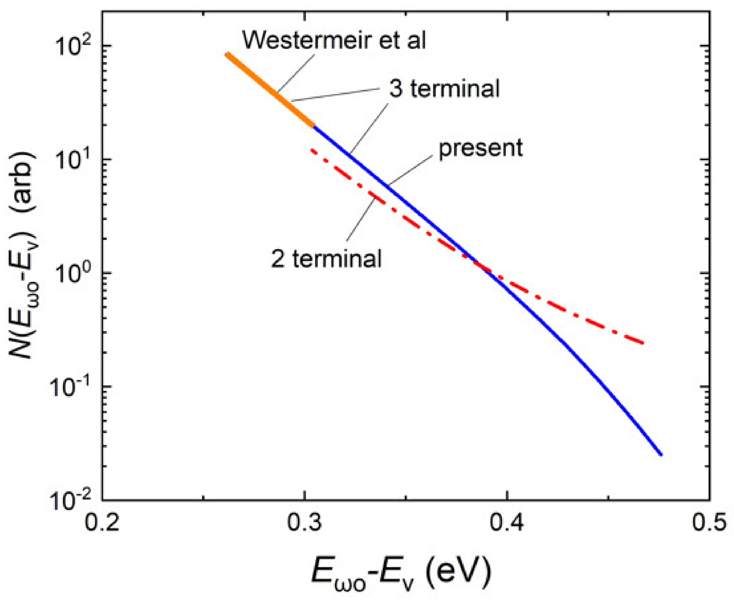
The tap distributions, as calculated according to Equation (7), are plotted in
Figure 5 as a function of the probed trap depth (
Eωo −
Ev) calculated from Equation (5). The
N(
Eωo −
Ev) distributions show a nearly exponential dependence with the indicative characteristic
Eo energies 35 meV and 30 meV at the shallower trap depths for the two- and three-terminal devices, respectively. At deeper trap depths, the trap distribution (blue solid line) of the FETs is found to be steeper than that of the two-terminal devices (red dashed-dotted line). It should be noted that the
N(
Eωo −
Ev) distribution of the FETs refers to the trap distribution of the first few pentacene monolayers at the insulator interface that make the dominant contribution to the
Ipo(ω) signal.
The role of the
cw bias illumination, on the other hand, in two-terminal devices is to excite an excess density of mobile holes in the valence band. These holes would quickly relax into the tail of localized states filling the exponential trap tail states, starting from the deepest levels (deep traps) and up to the characteristic energy level of the quasi-Fermi level of trapped holes
Etp. The more photocarriers produced, the more trap states in the tail are filled, and thus the closer the
Etp level gets to the transport path at the valence band edge at
Ev. This shift in the
Etp level is directly reflected in the MPC
Iac(
ω) spectra in
Figure 4d with the apparent shift to higher frequencies of the crossover frequency
ωs (vertical dashed lines). At
ωs, a crossover is observed where the
Iac(
ω) signal exhibits a transition from a strong to a much weaker frequency dependence before reaching a plateau or saturation at a lower
ω. This plateau signifies the so-called low frequency (LF) regime that occurs for
ω <<
ωt. The crossover frequencies
ωs are determined from the spectra of the
Iac(
ω)/
Iaco(
ω) ratio from
Figure 4e calculated by dividing the
Iac(
ω) spectra by the
Iaco(
ω) spectrum from
Figure 4d. It can be seen that each ratio
Iac(
ω)/
Iaco(
ω) in
Figure 4e is close to unity (horizontal solid line) at higher frequencies (
ω >>
ωt) that define the HF regime. Around each
ωs and lower frequencies, the
Iac(
ω)/
Iaco(
ω) ratio drops sharply following approximately a straight line. The extrapolation of this line intersects the horizontal solid line at the crossover frequency
ωs (down arrow), defining the crossover from the HF to the LF regime. The crossover frequency
ωs is used to determine the characteristic trapping frequency
ωt, considering that
ωt is approximately [
20]
The
ωt, from Equation (8) is introduced in the more general Equation (3) to determine the probe energy level
Eω, depicted in panel (f) in
Figure 4 (symbols), of the corresponding
Iac(
ω) spectra. By decreasing
ω below
ωs, the probed energy level
Eω in
Figure 4f shifts progressively slowly toward the corresponding quasi-Fermi level
Etp, (horizontal arrows). Finally, in the LF regime where the
Iac(
ω) has reached a plateau,
Eω is very close to
Etp and hardly shifts by changing
ω, confirming that the LF regime has indeed been reached and that Equation (8) is a good approximation. Moreover, Equation (8) can be introduced into Equation (4) to obtain
which is very useful as it provides an estimate of the energy gap (
Etp −
Ev). Taking advantage of this, we can determine the energy gap (
EF −
Ev). Particularly, in the case of the spectrum in
Figure 4d obtained with the lowest intensity of the bias light (open circles), the current under illumination is comparable to the dark current. Therefore, the corresponding quasi-Fermi
Etp level (horizontal dashed line) estimated at 0.56 eV above
Ev is very close to the Fermi level
EF and can be considered an estimation of the
EF level: (
Etp −
Ev) ≈ (
EF −
Ev) ≈ 0.56 eV.
It should be emphasized that the characteristic variations in the
Ip(
ω) spectra in
Figure 4a obtained by focusing the laser light beam at various positions along the transistor channel, are qualitatively very similar to the variations in the
Iac(
ω) spectra in
Figure 4d obtained by varying the intensity of the bias light. A crossover from the HF to the LF regime also occurs in the
Ip(
ω) spectra of three-terminal devices at the crossover frequency
ωs (vertical dashed lines). This frequency is determined from the ratio
Ip(
ω)/
Ipo(
ω) (
Figure 4b), as in the case of the two-terminal devices (
Figure 4e) described above. The corresponding characteristic trapping frequency
ωt can be then estimated from the frequency
ωs using Equation (8). Since the
ωs in
Figure 4a,b shifts to a higher frequency as the probe laser beam is placed progressively closer to the source, accordingly, the
ωt calculated from Equation (8) shifts progressively to a higher
ω.
3.5. Application of Our Analysis to the FR-SPCM Data of Other Authors
Photocurrent profiles
Ip(
x) along the channel of the FETs for different modulation frequencies
ω of the probe laser beam have been reported by Westermeir et al. [
12] and Fiebig [
22]. We digitized these results from which we extracted the frequency dependence of the photocurrent, i.e., the
Ip(
ω) spectra near the source (S), in the middle between the source and drain (M), and near the drain (D), as in our device. For comparison, these spectra were vertically shifted to match at higher
ω with each other and with the
Ip(
ω) spectra in
Figure 4a. The resulting
Ip(
ω) spectra of all devices are plotted in
Figure 7. From this figure, it is remarkable that the frequency dependence of the photocurrent
Ip(
ω) of all the different devices is very similar. In particular, by extrapolating at higher
ω, the upper envelope
Ipo(
ω) (solid green line) of our
Ip(
ω) spectra, we obtain the upper envelope
Ipo(
ω) (solid orange line) corresponding to the HF regime of the
Ip(
ω) spectra (open squares) of Westermeir et al. [
12]. These authors have performed SPCM measurements up to over ten times’ higher frequencies. The
N(
Eωο −
Ev) trap distribution derived from the
Ipο(
ω) spectra of Westermeir et al. [
12] via Equation (7) is also exponential with
Eo = 30 meV shown in
Figure 5 (orange solid line) and is the extension at shallower trap depths of the exponential
N(
Eωο −
Ev) distribution derived from our device.
In the
Ip(
ω) spectra in
Figure 7, the characteristic transition from the HF to the LF regime is observed in all devices. By decreasing the frequency below the respective crossover at
ωs, the
Ip(
ω) signal shows a very similar weak frequency dependence without, however, the characteristic saturation in the LF regime observed in the
iac(
ω) spectra of two-terminal devices (
Figure 4f). This can be attributed to the fact that the upward band bending in the pentacene accumulation layer vanishes within the Debye length
LD, which includes about 2–3 pentacene monolayers above the insulator interface. In the first monolayer, the upward band bending is the highest and thus this layer has the highest density of trapped holes and the highest effective contribution to the
Ip(
ω) signal. Therefore, the characteristic transition from the HF to the LF regime and the saturation of the photocurrent produced from the first monolayer are expected at relatively higher frequencies. The respective lower contribution to
Ip(
ω) from the subsequent monolayers with the lower band bending is expected to continue to increase with decreasing
ω and to saturate at lower frequencies. This may provide an increasing small contribution to the
Ip(
ω) signal at lower
ω that can explain the weak increase in the
Ip(
ω) signal in the LF regime.
Using Equation (9), we calculated the position of
Ev with respect to
Etp using the corresponding crossover frequencies
ωs, as determined from the
Ip(
ω) spectra in
Figure 7, and the results from all the devices are presented in
Figure 6. Similar to our device, the device of Westermeier et al. [
12] also operates in the saturation region by applying the same voltages
VGS = −20 V and
VDS = −10 V, and the
Ev edge from the drain to the source is also getting closer to the
Etp or
EF level. Therefore, an inhomogeneous upward band bending is confirmed along the channel, which is typical for transistors operating in the saturation region. In contrast, in Fiebig’s device [
22], operating in the linear region with
VGS = −30 V and
VDS = −5 V, the edge
Ev is at about the same energy below the
Etp or
EF level throughout the transistor channel (
Figure 6). This indicates that the valence band bends up uniformly along the channel providing a constant upward band bending, which is characteristic of FETs operating in the linear region. This uniform band bending is further supported by the nearly uniform photocurrent profile
Ip(
x) reported by Fiebig for this transistor operating in the linear region [
22].
Finally, it is important to note that in all the examined FETs presented in
Figure 6, the edge
Ev is located below the
EF level assuming either attempt-to-escape frequency
νο = 10
10 s
−1 or the relatively lower
νο = 10
8 s
−1. Therefore, the upward band bending for the applied
VGS = −20 V or −30 V is not sufficient for the
EF level to enter the valence band.


