Communication

A Ka-Band Doherty Power Amplifier in a 150 nm GaN-on-SiC Technology for 5G Applications

by
Alessandro Parisi
1,
Giuseppe Papotto
1,
Claudio Nocera
1,
Alessandro Castorina
1 and
Giuseppe Palmisano
2,*
1
STMicroelectronics, 95121 Catania, Italy
2
Dipartimento di Ingegneria Elettrica Elettronica e Informatica (DIEEI), University of Catania, 95125 Catania, Italy
*
Author to whom correspondence should be addressed.
Electronics 2023, 12(17), 3639; https://doi.org/10.3390/electronics12173639
Submission received: 27 July 2023 / Revised: 22 August 2023 / Accepted: 24 August 2023 / Published: 29 August 2023
(This article belongs to the Special Issue Recent Advances in RF and Millimeter-Wave Design Techniques)

Abstract

:
This paper presents a Ka-band three-stage power amplifier for 5G communications, which has been implemented in a 150 nm GaN-on-SiC technology and adopts a Doherty architecture. The amplifier is made up of a 50 Ω input buffer, which drives a power splitter, thanks to which it delivers its output power to the two power amplifier units of the Doherty topology, namely the main and auxiliary amplifier. Finally, the outputs of the two power amplifiers are properly arranged in a current combining scheme that enables the typical load modulation of the Doherty architecture, alongside allowing power combining at the final output. The proposed amplifier achieves a small signal gain of around 30 dB at 27 GHz, while providing a saturated output power of 32 dBm, with a power-added efficiency (PAE) as high as 26% and 18% at peak and 6 dB output power back-off, respectively.

1. Introduction

The 5G network is the key technology for the deployment of the next-generation communication systems. It envisages data rates of up to 100 Gbps, with ultra-low latency (i.e., lower than 1 ms), high reliability, and massive network capacity, with a simultaneous connection density higher than 1 M/km2. This will enable a wide range of breakthrough applications under various environments, such as healthcare, home automation, etc. [1,2,3].
To support the stringent requirements of such applications, the 5G network relies on carrier frequencies in the Ka-band and allows extended bandwidth and alternative access techniques, such as beam division multiple access (BDMA) and massive MIMO [4]. Furthermore, highly spectral efficient modulation schemes have been adopted (e.g., 64-QAM OFDM modulation) by 5G communication systems, which lead to transmission signals with a high peak-to-average power ratio (PAPR), thus pushing the power amplifier (PA) to operate in a deeper output power back-off (OPBO) region. This scenario poses stringent requirements to the PA, which mainly sets the efficiency and linearity performance of the whole transceiver [5]. Specifically, increasing the efficiency of the PA while preserving linearity is mandatory in a 5G transceiver for both the reduction in the operating costs of the base stations and the enhancement in the battery lifetime of the handsets. Moreover, a high output power (i.e., in the range of a few watts) in the Ka-band is required to the 5G power amplifiers to increase the network coverage area.
The Doherty architecture is the best candidate for the implementation of mm-wave power amplifiers for 5G applications. A Doherty power amplifier (DPA) is made up of a main and an auxiliary amplifier and exploits load modulation to provide an optimum trade-off between efficiency and linearity.
In recent years, several mm-wave DPAs that were designed using CMOS and BiCMOS technology have been presented [6,7,8]. These works demonstrate the effectiveness of the Doherty architecture to guarantee linearity while preserving efficiency, but they exhibit an output power that is well below the typical requirements of 5G applications, leading to the request for high-order MIMO architectures. On the other hand, gallium nitride (GaN) is nowadays the reference technology for the implementation of high-power and efficient power amplifiers. Although, over-W output power mm-wave DPAs in GaN technology have been already demonstrated [9,10,11,12,13,14], these works suffered from a limited gain performance. This means that they require a high input power, thus transferring to the pre-amplifier design requirements, such as output power, linearity, and efficiency.
In this work, the design and characterization of a Ka-band DPA for 5G applications has been presented. The amplifier exploits a three-stage architecture and provides a small signal gain of around 30 dB at 27 GHz, while achieving a saturated output power, PSAT, of 32 dBm with a power-added efficiency (PAE) as high as 26% and 18% at peak and 6 dB OPBO, respectively.
This paper has been organized as follows. Section 2 briefly discusses the Doherty operation, while Section 3 provides an insight on the GaN technology adopted and mainly deals with the DPA design and circuit solutions. Experimental results have been presented in Section 4, which also provides a comparison with the state of the art. Finally, conclusions have been drawn in Section 5.

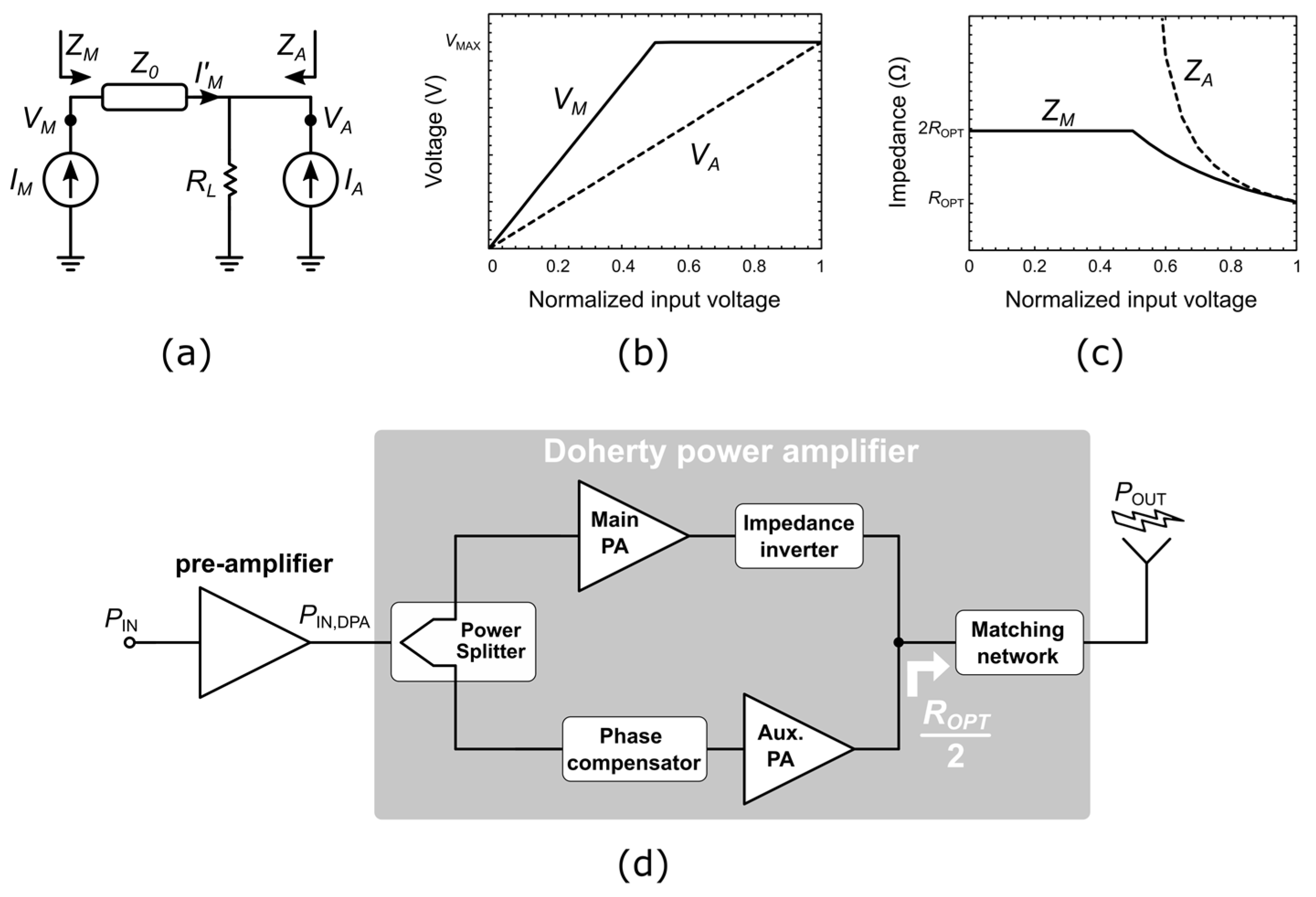
2. The Doherty Operation
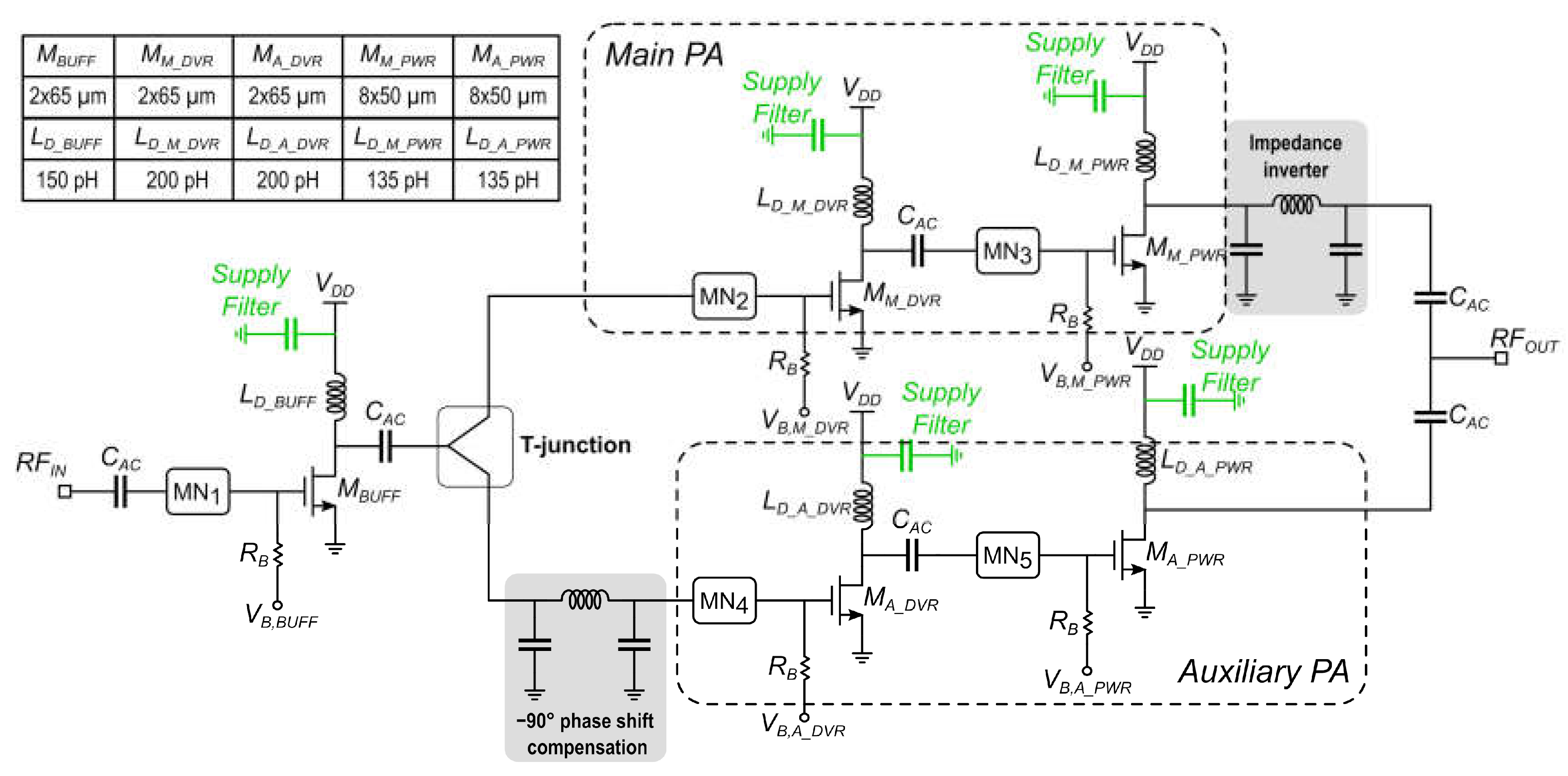
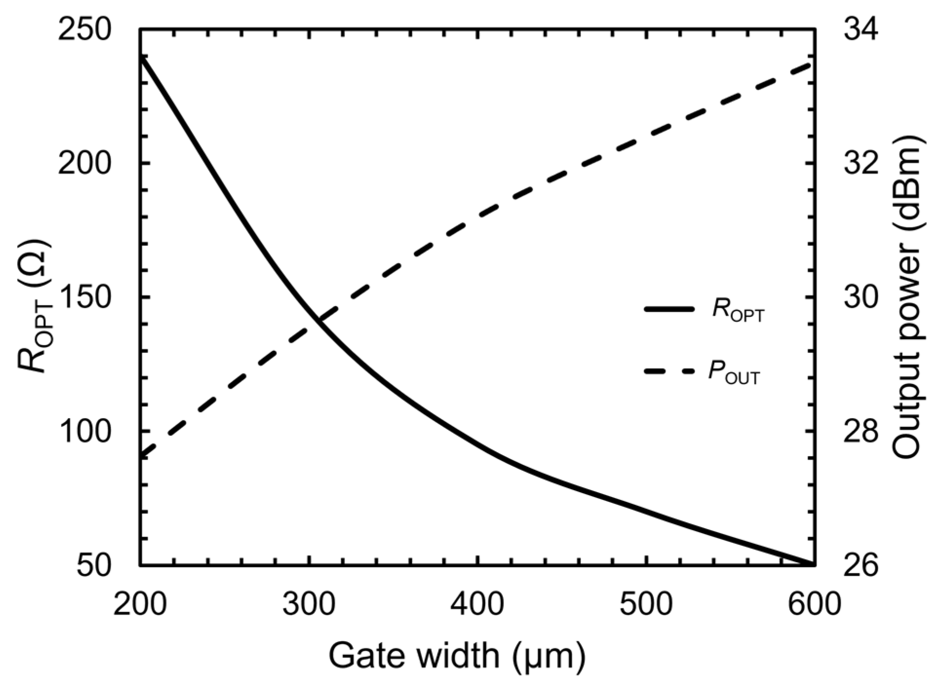
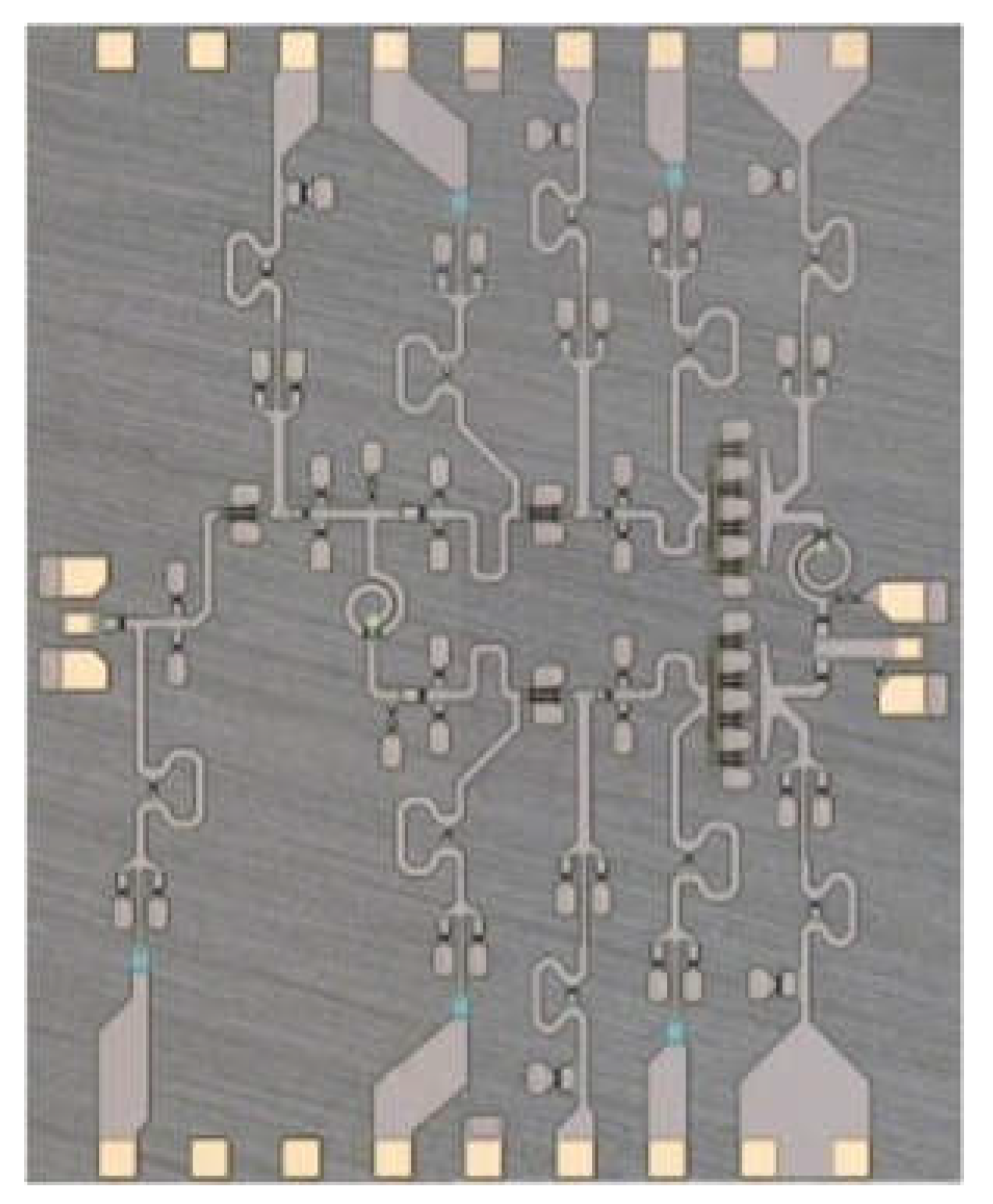
A Doherty power amplifier consists of a main and an auxiliary amplifier, which are properly arranged in a power-combining scheme to enable active load modulation and allow efficiency enhancement [15,16].
Figure 1a shows the well-known structure for the implementation of the Doherty architecture, which has been referred to as the current-combined DPA. The two current sources, IM and IA, represent the main and auxiliary amplifiers, respectively. The impedance-inverting network, which has been implemented through a quarter-wave transmission line with characteristic impedance Z0, combines the power from both amplifiers into the load, RL, and simultaneously downscales the impedance observed by IM for optimum efficiency performance [15]. The load impedance of the main amplifier is modulated through the current of the auxiliary amplifier, as according to Equation (1):
Z M = Z 0 2 R L ( 1 + I A I M ' )
where I′M is the current of the main amplifier that has been transformed via the impedance-inverting network. In the Doherty operation, the main and the auxiliary amplifier are usually operated in class AB and C [17,18,19,20,21], respectively. Therefore, a low (i.e., until OPBO) and a high (i.e., from OPBO to saturation) power region can be identified. In the low-power region, only the main amplifier is active and provides current to the load; in the high-power region, both amplifiers are active and load modulation properly occurs. Specifically, in the low-power region, according to Equation (1), the main amplifier output load is ZM = Z02/RL (IA = 0), and its output voltage, VM, linearly increases with the driving input voltage, Vi, until reaching its maximum value and, hence, its first peak of efficiency. As Vi increases, the auxiliary amplifier turns on and modulates the load impedance of the main amplifier to keep VM to its maximum value and simultaneously increasing the output power. Once the output voltage of the auxiliary amplifier, VA, reaches its maximum value, a second peak of efficiency occurs, which defines the saturation condition. Assuming a symmetrical Doherty configuration (i.e., the two amplifiers generating the same maximum current) Z0 and RL are to be set to ROPT and ROPT/2, respectively, where ROPT is the optimum impedance of the amplifiers [20]. Figure 1b,c show the voltage and load impedance profile, respectively, versus the normalized input voltage for both amplifiers. It is worth noting that the load impedance of the main amplifier is modulated from 2ROPT to ROPT, whereas its output voltage is kept constant at its maximum value thanks to the load modulation. On the other hand, the load impedance of the auxiliary amplifier changes from ideally infinity to ROPT.
The simplified schematic of a DPA is shown in Figure 1d, which includes an input power splitter to drive both amplifiers, a phase compensator to compensate for the phase shift introduced by the impedance inverter, and an output matching network to transform the 50 Ω impedance of the antenna into the required Doherty load impedance (i.e., RL = ROPT/2).

3. Circuit Design

The proposed DPA was designed using GaN-on-SiC technology, which features a substrate thickness of 100 μm and provides high-electron-mobility transistors (HEMTs) with a gate length of 150 nm. These devices exhibit a transition frequency of 35 GHz, manage a power density of about 3 W/mm, and are defined via a scalable non-linear model qualified up to a 20 V operating drain voltage. As far as the back end of line (BEOL) is concerned, this technology provides two gold metal layers with a thickness of 1 µm and 4 µm, MIM capacitors with specific capacitance of around 215 pF/mm2, and 50 Ω/square thin-film resistors. Moreover, it features through-wafer vias for low-inductance ground connections and air-bridge-based passive structures for optimum monolithic inductors.
A simplified schematic of the proposed Ka-band DPA is shown in Figure 2. It is based on a three-stage architecture, which allows a linear gain as high as 30 dB to be achieved. Specifically, the DPA is made up of a 50 Ω input buffer and two power units, namely the main and auxiliary PAs, which, in turn, are composed of a driver and a power stage. The input buffer supplies both the main and auxiliary branches by means of a proper power splitter connected to the driver inputs, whereas the power output terminals are arranged in a current combining scheme, which includes the impedance inverter for proper load modulation.
Distinct from the conventional implementation (see Figure 1d), here the output matching network that transforms the 50 Ω load into the impedance required by the Doherty architecture (i.e., ROPT/2 in Figure 1d) [22] has been avoided. In this way, all the limitations related to this matching network in terms of power loss, area occupation, and bandwidth have been overcome. Figure 3 shows a 28 GHz load-pull simulation for a transistor whose gate width ranges from 200 to 600 μm. This simulation provides the optimum load resistance, ROPT, and the corresponding output power, POUT, assuming a class AB operation.
It is important to note that only the imaginary part of the optimum load needs to be tuned to the operating frequency, whereas the real part is not appreciably affected by the frequency. As apparent, a transistor with a gate width of 400 µm needs an optimum load of 100 Ω, which allows the output matching network to be avoided. Accordingly, a 400 µm transistor with eight gate fingers, each of 50 µm, was used for both the main and auxiliary power stages, thus implementing a symmetrical Doherty configuration with the aim of achieving an OPBO of 6 dB. Neglecting impedance inverter losses and assuming a 31 dBm output power (see Figure 3) for each power stage, a maximum output power of 34 dBm is achieved. A gate width of 130 µm (i.e., 2 × 65 µm) was set for both the input buffer and driver stages as a fair trade-off between driving capability and power consumption, with the aim of preserving PAE performance. Moreover, shunt inductors, LD, are sized to absorb the residual drain parasitic capacitance of the transistors, which are not compensated through the interstage matching networks (MNs), thus improving the frequency performance. Although a symmetrical configuration, the main and auxiliary amplifiers differ in their class of operation. Specifically, the main PA stages are operated in class AB by setting the gate-source voltage to around −1.7 V, while the auxiliary PA stages are operated in deep class C with the gate-source voltage at around −2.2 V.
As far as the design of passive structures is concerned, a lumped-based approach was preferred over the distributed one, with the aim of reducing area occupation. Specifically, the impedance inverter at the output of the main power stage was implemented through exploiting a π network, whereas the power splitter was based on a T-junction architecture with a splitting factor of 1:1.5 for the main and auxiliary branches, respectively. Accordingly, a π network was included at the input of the auxiliary path to compensate for the 90° phase shift caused by the impedance inverter.
Figure 4 shows the passive circuitry of the designed DPA, which includes inductors, capacitors, through-wafer vias, and interconnections among components. All the inductors were designed by stacking the two metal layers available in the adopted technology, thus increasing the Q-factor. The layout of the overall amplifier was partitioned into four entries for EM simulation purposes, with the aim of accurately estimating interconnection parasitics and undesired coupling effects.
An S-parameter model of each entry of the EM simulator was extracted and embedded into the main schematic to finely tune transistor aspect ratios and matching networks for the optimum PA performance.

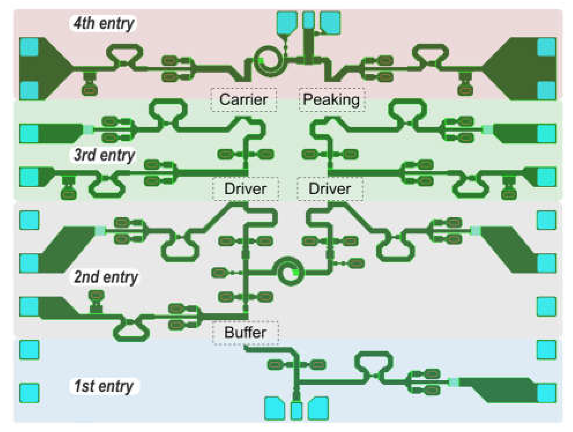
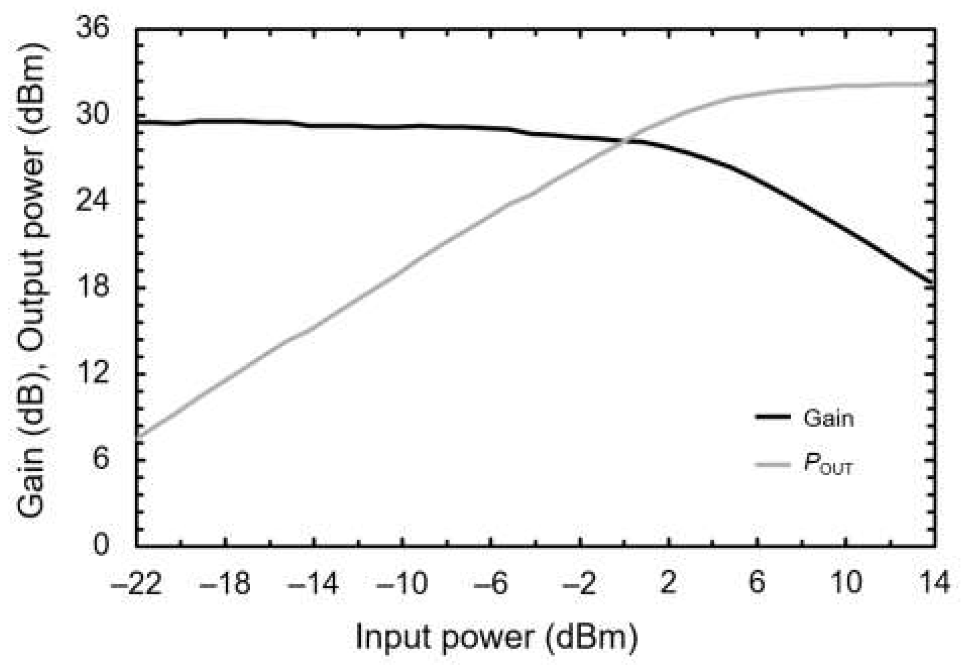
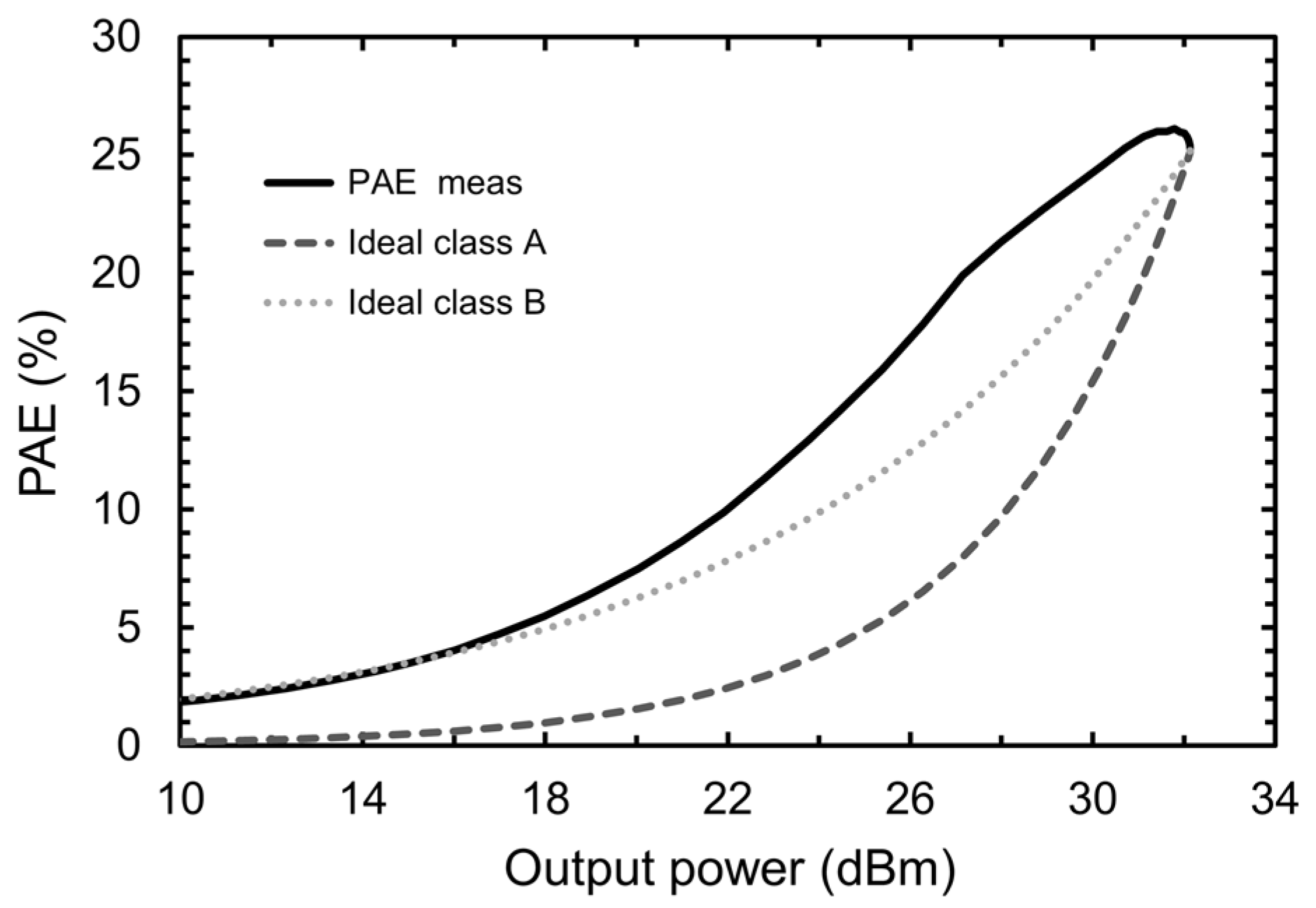
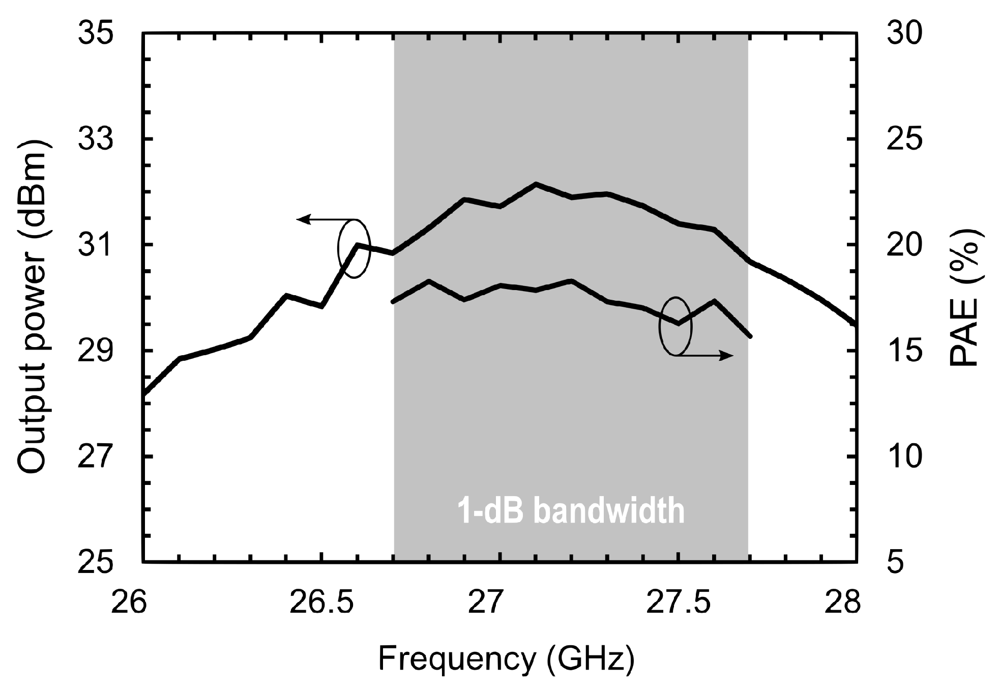
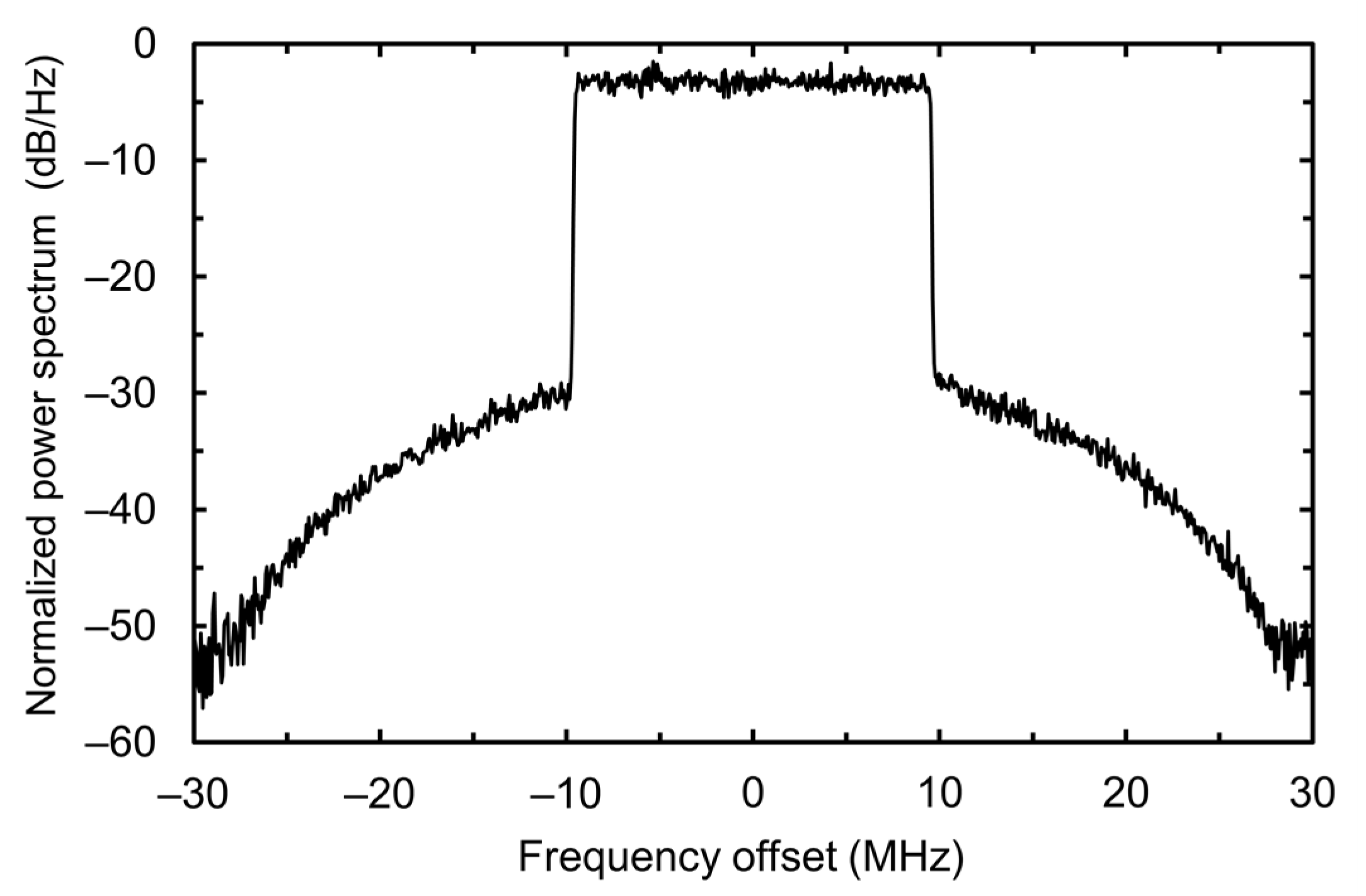
4. Experimental Results

Figure 5 shows the chip micrograph of the proposed Ka-band DPA, whose die size is 3.1 mm × 2.5 mm. Extensive on-wafer measurements were performed using a Cascade probe station to characterize the power amplifier. Specifically, bias voltages and mm-wave signals were directly probed on the die by means of dedicated on-chip pads.
For the sake of completeness, Figure 6 shows the adopted measurement setup, in which the mm-wave input signal is provided by a R&S SMW200A vector signal generator, whereas the amplifier output signal is delivered by means of a Keysight 87301C directional coupler to the Agilent E4417A power meter for power measurements and the Keysight UXA N9040B signal analyzer for spectrum analysis. All measurements were performed using a 20 V power supply under a continuous wave (CW) mode.
Figure 7 shows the measured S-parameters. As apparent from Figure 7a, good values of input (−S11) and output (−S22) return losses were achieved, which were both better than 10 dB at the operating frequency of 27 GHz. Moreover, the measured reverse isolation (−S12) was higher than 40 dB, and a small-signal gain (S21) as high as 30 dB was obtained, as shown in Figure 7b.
Figure 8 shows the measured output power and gain as a function of the input power at 27 GHz. As apparent, the proposed DPA delivered a maximum output power of about 32 dBm, while achieving linear and saturated gains as high as 30 dB and 22 dB, respectively.
Figure 9 compares the measured PAE at 27 GHz with the efficiencies of ideal class-A and class-B amplifiers, which have all been assumed with an equal PAE at PSAT. A peak PAE of 26% was achieved while, thanks to the Doherty operation, the PAE at 6 dB OPBO was about 18%, which is higher by factors of 2.75 and 1.4 than the PAE of the ideal class-A and class-B PAs, respectively.
Figure 10 shows the measured saturated output power over a frequency range from 26 GHz to 28 GHz. The DPA exhibits a 1 dB bandwidth of around 1 GHz. The PAE for the 6 dB OPBO in the 1 dB bandwidth has also been shown; it is almost flat, being around 18%.
PSAT was measured over all available samples (i.e., 30 samples) distributed on the same wafer for a statistical evaluation. The result is shown in Figure 11. As apparent, the average PSAT and its standard deviation, σ, are around 31.8 dBm and 0.5 dB, respectively.
The DPA was also characterized with a 64-QAM 5G NR downlink-modulated signal to assess its inherent linearity. This signal exhibited a PAPR of around 11 dB. The signal bandwidth was set to 20 MHz due to the frequency limitations of the available measurement setup. Figure 12 and Figure 13 show the measured received constellation and normalized output power spectrum. An EVM and an ACPR lower than 5% and −32 dBc were achieved, respectively, with an average output power, POUT,AVG, of 19 dBm. Moreover, the proposed DPA met the 5G linearity requirements [23], i.e., an EVM < 8% and an ACPR < −28 dBc, with a POUT,AVG of up to 21 dBm.
Finally, Table 1 summarizes the DPA experimental results, while comparing them with the state-of-the-art Ka-band GaN works. A higher PAE performance has been reported by the authors of [12,13], while the authors of [9,11,12] achieved a higher output power level. However, all these works exhibited a much lower gain performance, which greatly increased their pre-amplifier requirements in terms of maximum output power, linearity, and efficiency, thus negatively affecting the system complexity and cost in addition to the overall transmitter performance.
For a fair comparison, the following figure of merit (FoM), was used:
FoM   [ W mm 2 ] = P SAT × G SAT × P A E MAX × P A E 6 dB d i e   s i z e  
As apparent, the proposed DPA offers the best trade-off between the performance parameters, such as power density, saturated gain, and PAE.

5. Conclusions

This paper presents a Ka-band Doherty power amplifier implemented in a 150 nm GaN-on-SiC technology. The amplifier is based on a three-stage architecture and was designed with the aim of providing both a high output power and a high gain with suitable PAE performance to properly address the crucial issues of 5G GaN PAs. Extensive on-wafer measurements were carried out, including a statistical analysis that proved the robustness of the DPA design. The amplifier delivers up to 32 dBm with a PAE of 26%, while guaranteeing an excellent saturated gain as high as 22 dB. Finally, measurements with a 5G-modulated signal were carried out, achieving an EVM < 8% and an ACPR < −28 dB, with an average output power of 21 dBm.

Author Contributions

Conceptualization, A.P., G.P. (Giuseppe Papotto) and G.P. (Giuseppe Palmisano); methodology, A.P., C.N. and G.P. (Giuseppe Papotto); validation, A.C., A.P. and G.P. (Giuseppe Papotto); formal analysis, A.P. and C.N.; investigation, A.P., C.N. and A.C.; writing—original draft preparation, A.P. and G.P. (Giuseppe Papotto); writing—review and editing, A.P. and G.P. (Giuseppe Palmisano); supervision, G.P. (Giuseppe Papotto); project administration, G.P. (Giuseppe Palmisano). All authors have read and agreed to the published version of the manuscript.

Funding

This research received no external funding.

Data Availability Statement

The data presented in this study are available on request from the corresponding author.

Conflicts of Interest

The authors declare no conflict of interest.

References

  1. Erunkulu, O.O.; Zungeru, A.M.; Lebekwe, C.K.; Mosalaosi, M.; Chuma, J.M. 5G Mobile Communication Applications: A Survey and Comparison of Use Cases. IEEE Access 2021, 9, 97251–97295. [Google Scholar] [CrossRef]
  2. Agiwal, M.; Roy, A.; Saxena, N. Next generation 5G wireless networks: A comprehensive survey. IEEE Commun. Surv. Tutor. 2016, 18, 1617–1655. [Google Scholar] [CrossRef]
  3. Parvez, I.; Rahmati, A.; Guvenc, I.; Sarwat, A.I.; Dai, H. A survey on low latency towards 5G: RAN, core network and caching solutions. IEEE Commun. Surv. Tutor. 2018, 20, 3098–3130. [Google Scholar] [CrossRef]
  4. Gupta, A.; Jha, R.K. A survey of 5g network: Architecture and emerging technologies. IEEE Access 2015, 3, 1206–1232. [Google Scholar] [CrossRef]
  5. Asbeck, P.M. Will doherty continue to rule for 5g? In Proceedings of the 2016 IEEE MTT-S International Microwave Symposium (IMS), San Francisco, CA, USA, 22–27 May 2016; pp. 1–4. [Google Scholar]
  6. Yu, C.; Feng, J.; Zhao, D. A 28-GHz Doherty power amplifier with a compact transformer-based quadrature hybrid in 65-nm CMOS. IEEE Trans. Circuits Syst. II Exp. Briefs 2021, 68, 2790–2794. [Google Scholar] [CrossRef]
  7. Wang, D.; Chen, W.; Chen, X.; Liu, X.; Ghannouchi, F.M.; Feng, Z. A 24–29.5 GHz Voltage-Combined Doherty Power Amplifier Based on Compact Low-Loss Combiner. IEEE Trans. Circuits Syst. II Exp. Briefs 2021, 68, 2342–2346. [Google Scholar] [CrossRef]
  8. Ma, Z.; Ma, K.; Wang, K.; Meng, F. A 28 GHz Compact 3-Way Transformer-Based Parallel-Series Doherty Power Amplifier with 20.4%/14.2% PAE at 6-/12-dB Power Back-off and 25.5 dBm PSAT in 55nm Bulk CMOS. In Proceedings of the 2022 IEEE International Solid- State Circuits Conference (ISSCC), San Francisco, CA, USA, 20–26 February 2022; pp. 320–322. [Google Scholar]
  9. Piacibello, A.; Camarchia, V.; Colantonio, P.; Giofrè, R. 3-Way Doherty Power Amplifiers: Design Guidelines and MMIC Implementation at 28 GHz. IEEE Trans. Microw. Theory Tech. 2022, 71, 2016–2028. [Google Scholar] [CrossRef]
  10. Guo, R.; Tao, H.; Zhang, B. A 26 GHz Doherty power amplifier and a fully integrated 2 × 2 PA in 0.15 μm GaN HEMT process for heterogeneous integration and 5G. In Proceedings of the 2018 IEEE MTT-S International Wireless Symposium (IWS), Chengdu, China, 6–10 May 2018; pp. 1–4. [Google Scholar]
  11. Nakatani, K.; Yamaguchi, Y.; Komatsuzaki, Y.; Sakata, S.; Shinjo, S.; Yamanaka, K. A Ka-band high efficiency Doherty power amplifier MMIC using GaN-HEMT for 5G application. In Proceedings of the 2018 IEEE MTT-S International Microwave Workshop Series on 5G Hardware and System Technologies (IMWS-5G), Dublin, Ireland, 30–31 August 2018; pp. 1–3. [Google Scholar]
  12. Yamaguchi, Y.; Nakatani, K.; Shinjo, S. A wideband and high efficiency Ka-band GaN Doherty power amplifier for 5G communications. In Proceedings of the 2020 IEEE BiCMOS and Compound Semiconductor Integrated Circuits and Technology Symposium (BCICTS), Monterey, CA, USA, 16–19 November 2020; pp. 1–4. [Google Scholar]
  13. Giofre, R.; Gaudio, A.D.; Ciccognani, W.; Colangeli, S.; Limiti, E. A GaN-on-Si MMIC Doherty power amplifier for 5G applications. In Proceedings of the 2018 Asia-Pacific Microwave Conference (APMC), Kyoto, Japan, 6–9 November 2018; pp. 971–973. [Google Scholar]
  14. Wohlert, D.; Peterson, B.; Kywe, T.R.M.; Ledezma, L.; Gengler, J. 8-Watt Linear Three-Stage GaN Doherty Power Amplifier for 28 GHz 5G Applications. In Proceedings of the 2019 IEEE BiCMOS and Compound Semiconductor Integrated Circuits and Technology Symposium (BCICTS), Nashville, TN, USA, 3–6 November 2019; pp. 1–4. [Google Scholar]
  15. Zhao, C.; Liu, H.; Wu, Y.; Kang, K. Analysis and Design of CMOS Doherty Power Amplifier Based on Voltage Combining Method. IEEE Access 2017, 5, 5001–5012. [Google Scholar] [CrossRef]
  16. Srirattana, N.; Raghavan, A.; Heo, D.; Allen, P.E.; Laskar, J. Analysis and design of a high-efficiency multistage Doherty power amplifier for wireless communications. IEEE Trans. Microw. Theory Technol. 2005, 53, 852–860. [Google Scholar] [CrossRef]
  17. Reynaert, P.; Cao, Y.; Vigilante, M.; Indirayanti, P. Doherty techniques for 5G RF and mm-wave power amplifiers. In Proceedings of the 2016 International Symposium on VLSI Technology, Systems and Application (VLSI-TSA), Hsinchu, Taiwan, 25–27 April 2016; pp. 1–2. [Google Scholar]
  18. Nasri, A.; Estebsari, M.; Toofan, S.; Piacibello, A.; Pirola, M.; Camarchia, V.; Ramella, C. Broadband Class-J GaN Doherty Power Amplifier. Electronics 2022, 11, 552. [Google Scholar] [CrossRef]
  19. Cheng, P.; Wang, Q.; Li, W.; Jia, Y.; Liu, Z.; Feng, C.; Jiang, L.; Xiao, H.; Wang, X. A Broadband Asymmetrical GaN MMIC Doherty Power Amplifier with Compact Size for 5G Communications. Electronics 2021, 10, 311. [Google Scholar] [CrossRef]
  20. Zong, Z.; Tang, X.; Khalaf, K.; Yan, D.; Mangraviti, G.; Nguyen, J.; Liu, Y.; Wambacq, P. A 28 GHz Voltage-Combined Doherty Power Amplifier with a Compact Transformer-based Output Combiner in 22nm FD-SOI. In Proceedings of the 2020 IEEE Radio Frequency Integrated Circuits Symposium (RFIC), Los Angeles, CA, USA, 4–6 August 2020; pp. 299–302. [Google Scholar]
  21. Abounemra, A.M.E.; Chen, W.; Huang, F.; Maktoomi, M.; Zhang, W.; Helaoui, M.; Ghannouchi, F.M. Systematic Design Methodology of Broadband Doherty Amplifier Using Unified Matching/Combining Networks with an Application to GaN MMIC Design. IEEE Access 2021, 9, 5791–5805. [Google Scholar] [CrossRef]
  22. Zong, Z.; Tang, X.; Khalaf, K.; Yan, D.; Mangraviti, G.; Nguyen, J.; Liu, Y.; Wambacq, P. A 28-GHz SOI-CMOS Doherty power amplifier with a compact transformer-based output combiner. IEEE Trans. Microw. Theory Technol. 2021, 69, 2795–2808. [Google Scholar] [CrossRef]
  23. Generation Partnership Project; Technical Specification Group Radio Access Network; NR; Base Station (BS) Radio Transmission and Reception (Release 15). Standard TS 38.104, 3rd Generation Partnership Project-3GPP. v.15.5.0. Section 9. 2019. Available online: https://www.etsi.org/deliver/etsi_ts/138100_138199/138104/15.05.00_60/ts_138104v150500p.pdf (accessed on 1 March 2019).
Figure 1. Doherty operating principle: (a) current combined structure, (b) corresponding voltages versus the normalized input voltage, (c) corresponding load impedances versus the normalized input voltage, and (d) simplified schematic of a Doherty power amplifier.
Electronics 12 03639 g001
Figure 2. Simplified schematic of the proposed Ka-band DPA.
Electronics 12 03639 g002
Figure 3. Load-pull simulations of a GaN transistor versus the gate width: optimum load resistance and delivered output power at 28 GHz.
Electronics 12 03639 g003
Figure 4. Passive circuitry of the Doherty power amplifier.
Electronics 12 03639 g004
Figure 5. Chip microphotograph of the Ka-band DPA.
Electronics 12 03639 g005
Figure 6. DPA measurement setup.
Electronics 12 03639 g006
Figure 7. Measured S-parameters: (a) input (-S11) and output (-S22) return loss, and (b) small-signal gain (S21) and reverse isolation (-S12).
Electronics 12 03639 g007
Figure 8. Measured POUT and gain as a function of PIN.
Electronics 12 03639 g008
Figure 9. Measured PAE as a function of POUT, along with a comparison of efficiency between the ideal class-A and class-B PAs.
Electronics 12 03639 g009
Figure 10. Delivered output power as a function of the frequency and 6 dB OPBO PAE over the 1 dB bandwidth.
Electronics 12 03639 g010
Figure 11. Distribution of the saturated output power over 30 samples.
Electronics 12 03639 g011
Figure 12. Measured received constellation at POUT,AVG = 19 dBm.
Electronics 12 03639 g012
Figure 13. Measured normalized power spectrum at POUT,AVG = 19 dBm.
Electronics 12 03639 g013
Table 1. Performance comparison with the state-of-the-art Ka-band DPAs.
[9][10][11][12][13]This Work
Channel length [nm]150 *150 *150 *150 *100 **150 *
Frequency [GHz]282628302827
PSAT [dBm]343235.636.53332.1
Linear gain [dB]2013.615.815.713.730
Saturated gain [dB]108121012.522
PAEMAX [%]2221.725.531.836.226
PAE @ 6 dB OPBO [%]152022.7273018
VDD [V]202424241220
Die size [mm2]15.654.33.567.75
FoM [W/mm2]0.050.090.771.10.641.5
* GaN-on-SiC; ** GaN-on-Si.
Disclaimer/Publisher’s Note: The statements, opinions and data contained in all publications are solely those of the individual author(s) and contributor(s) and not of MDPI and/or the editor(s). MDPI and/or the editor(s) disclaim responsibility for any injury to people or property resulting from any ideas, methods, instructions or products referred to in the content.

