Article

A 12-Bit 1-GS/s Pipelined ADC with a Novel Timing Strategy in 40-nm CMOS Process

1
School of Microelectronics, University of Chinese Academy of Sciences, Beijing 100049, China
2
Institute of Microelectronics of the Chinese Academy of Sciences, Beijing 100029, China
3
Acela Microelectronics Co., Ltd., Suzhou 215124, China
*
Authors to whom correspondence should be addressed.
Electronics 2023, 12(4), 924; https://doi.org/10.3390/electronics12040924
Submission received: 21 January 2023 / Revised: 8 February 2023 / Accepted: 10 February 2023 / Published: 12 February 2023

Abstract

:
This paper presents a 1-GS/s12-bit pipelined analog-to-digital converter (ADC) fabricated in 40-nm CMOS technology that optimizes the settling time, bit error rate, and robustness. This ADC uses an improved timing called pre-quantization timing (PQT), which implements quantization in half the time of the sampling phase to maximize the output-settling time of the operational amplifier (op-amp). A complete clocking scheme along with a delay lock loop (DLL) is proposed to generate an accurate timing no matter how process, voltage, and temperature (PVT) change. Based on PQT, a high-speed comparator circuit is adopted to obtain a bit error rate (BER) below 10−15. Sample and hold amplifier (SHA) is used to guarantee robustness over the wide input frequency. Furthermore, a low-cost automatic calibration is implemented to correct residual curves, and inter-stage gain errors are also corrected. This ADC achieves a signal-to-noise-and-distortion ratio (SNDR) of 57.3 dB and a spurious-free dynamic range (SFDR) of 78.5 dB at a 227 MHz input frequency. The measured differential nonlinearities (DNL) and integral nonlinearities (INL) after calibration are ±0.7 LSB and ±1.50 LSB, respectively. The power consumption of the ADC core is 97.6-mW, and the Walden figure of merit (FoM) is 172.9-fJ/conversion-step.

1. Introduction

Driven by the rapid development of the information age, the demand for systems such as data acquisition, future mobile communication systems, and instrumentation is growing rapidly [1,2,3,4]. As the core devices of these systems, high-speed and high-precision ADCs with a resolution exceeding 10-bit and a sampling rate higher than 1-GS/s have become a research hotspot [5,6,7]. However, at a high sampling rate, too short a settling time makes the settling of the residual amplifier (RA) insufficient, resulting in a decrease in ADC performance. The output-settling time of the operational amplifier is affected not only by the performance of the operational amplifier but also by the other modules such as comparators, switch capacitors, clocks, etc. In recent years, there have been several solutions to the problem of insufficient settling time of op-amps. Firstly, the ring amplifier, due to its simple topology and low power consumption, replaces the traditional operational amplifier [8,9]. A ring amplifier combined with a high-pass filter can improve the settling time [8]. Second, the effective settling time of the residual amplifier is limited by the resolving time of the sub-ADC, so there are numerous studies on improving the performance comparators [10]. For example, an improved high-speed dynamic comparator is adopted, which aims to optimize the comparator’s regeneration time and reset time [11]. Thirdly, choosing a reasonable switch resistance to create a critically damped system can reduce the multiplication time of the digital-to-analog converter (MDAC) [12]. In addition, an optimized MDAC was introduced to eliminate the effects of insufficient settlement between adjacent samples in conventional MDACs [13]. In general, great progress has been made in the improvement in settling time; however, optimization in timing from a timing perspective, which directly allocates more time to op-amps, has not been adequately studied.
To address the issue, this paper proposes a reasonable and improved working timing called pre-quantization timing (PQT). Different from traditional timing that includes the sampling phase and the amplification phase, the PQT is divided into three stages: sampling, pre-quantization, and amplification, which brings obvious advantages as follows. First of all, PQT solves the problem of not allocating enough time for quantization in traditional timing. Second, a small cost is sacrificed to allow for more time for the op-amps to settle. Third, the bit error rate of the chip can be considerably reduced when employing a high-speed comparator, and the bit error rate is near 10−15 in the final testing and verification.
However, the main difficulties of the above timing applications are as follows: On the one hand, the clock generation circuit has difficulty in generating an accurate and stable timing of 25% duty cycle. Traditional pipelined ADCs using this timing typically operate in time-domain interleaved mode, as shown in the article [14,15]. On the other hand, the external 2-GHz input clock mentioned by previous studies on pipelined ADCs increases the application difficulty of the system [16]. Therefore, this ADC uses a delay lock loop (DLL)-dependent clock circuit to generate the above timing, which can provide a non-50% duty cycle clock phase without an additional master clock. On the other hand, although PQT makes the design of the input buffer more challenging, it is less difficult than the design of the closed-loop op-amp of the MDACs, so this design is feasible and desirable.
In addition to the PQT mentioned above, the performance of the modules in ADC core should also be carefully designed. Firstly, DLL is mainly used to generate a precise time delay, which does not change with external conditions such as temperature and voltage [17]. The variable delay line (VDL) is used to configure different sampling rates to provide a stable and reliable comparator clock. The comparator is a key module of the pipelined ADC, and its speed and precision directly determine the performance that the ADC can achieve. Secondly, a four-input comparator combined with threshold offset calibration is designed for high-speed and high-precision performance. For the offset of the comparator, this paper corrects the threshold offset of the comparator by adjusting the bias current of the preamplifier [18]. In theory, adding adjustable current sources at the input can directly adjust the offset voltage, but it is difficult to turn off the switches. Therefore, it is more appropriate to add an adjustable current source at the output ports. This paper calculates the equivalent input offset voltage after introducing the bias current and displays it in the form of a picture. Thirdly, the sample-and-hold amplifier (SHA)-less architecture is known for its low power consumption and low ADC noise, but the performance of IF-sampling ADCs degrades due to the aperture error at high-input frequencies [19,20,21]. Overall, SHA is worth choosing for better sampling linearity and robustness. In addition, sampling with a bootstrap switch exhibits higher linearity and faster speed than MOS or CMOS switches. Fourth, operational amplifiers for MDAC circuits are required to increase swing, gain, and bandwidth.
Both foreground and background calibrations have been used to correct errors and mismatches in this ADC. Firstly, this ADC adopts the method of automatic calibration by plotting a residual curve to calibrate the residual curve. [22]. This ADC investigates automatic calibration for residual curve calibration, which avoids the time-consuming and difficult manual adjustment. Second, the finite inter-stage gain of the MDAC is calibrated by injecting dither in the first three stages. Because the code–domain equalization calibration technology greatly increases the power consumption and complexity of analog circuits, this design uses pseudo-random noise injection calibration by directly adding a small amount of capacitance and voltage [23,24]. The injection position is more flexible and can effectively improve the spectrum.
This paper is organized as follows: Section 2 introduces the architecture of the whole ADC, especially the proposed pre-quantization timing. In Section 3, the circuit implementation and calibration of the 1 GS/s 12-bit pipelined ADC is described in detail. Section 4 offers a detailed discussion along with measured results for future work. Finally, conclusions are provided in Section 5.

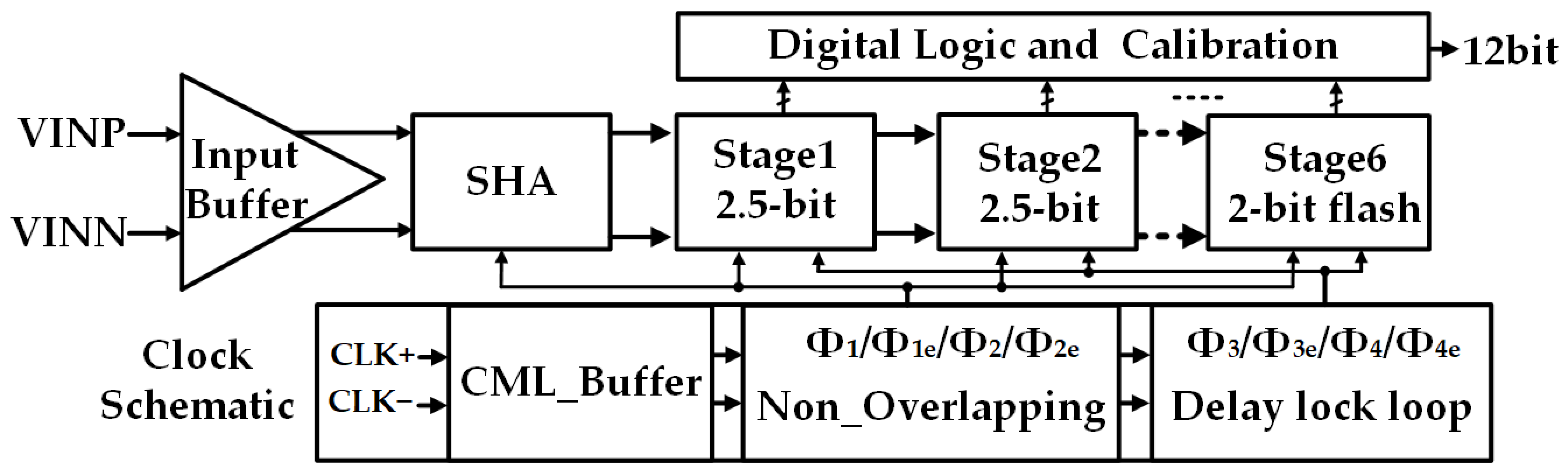
2. Proposed ADC Architecture and Pre-Quantization Timing

2.1. ADC Architecture

The block diagram of the proposed 1 GS/s 12-bit ADC with pre-quantization timing is presented in Figure 1. An input buffer is placed at the front end in this design. First, the high-input impedance makes the ADC easier to drive, and the low-output impedance enables the sampling channel to obtain a larger bandwidth, especially at high frequencies, which is beneficial for improving the sampling linearity. The second advantage is isolating the kickback noise from the ADC sampling path. The input buffer current is in the mA range, and the performance of the input buffer with low-frequency input is inversely proportional to the current; that is, lowering the current helps improve the linearity of the low-input frequency while also lowering overall power consumption. The SHA follows the input buffer. The performance of SHA is relatively stable under the full input frequency and PVT, although SHA brings extra power consumption and nonlinearity to some extent. Bootstrapped switches, together with SHA, follow the input buffer to improve the sampling linearity and achieve better robustness. Based on PQT timing, the input signal is digitized by five cascading MDACs, where the ten most significant bits are resolved by five cascading 2.5-bit MDACs, and the two least significant bits are determined by a 2-bit flash ADC. Additionally, the clock schematic, combined with the high-speed interface current mode logic (CML), non-overlapping clock, and DLL, provides the needed timing. (Ф1, Ф1e, Ф2, Ф2e, Ф3, Ф3e, Ф4, and Ф4e).

2.2. Working Timing Strategy

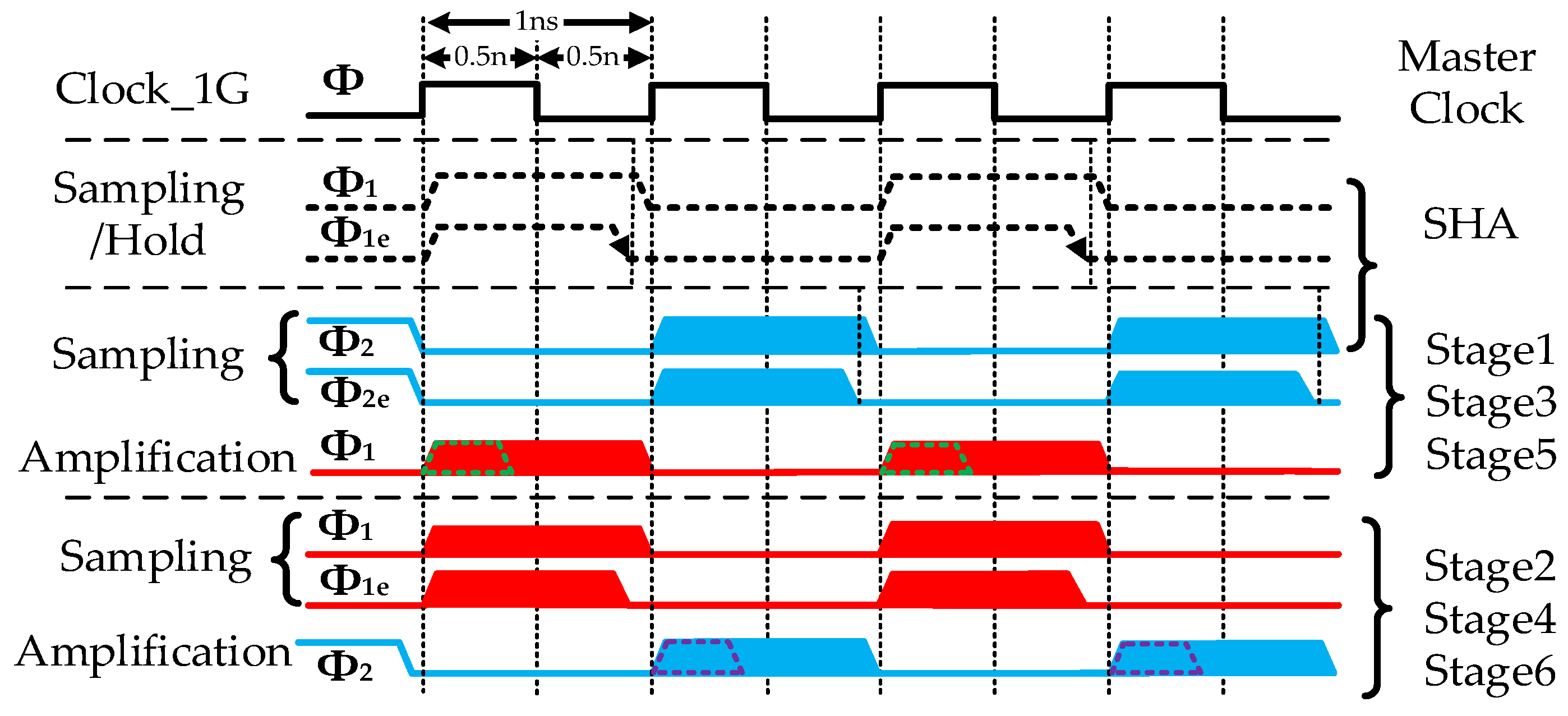
2.2.1. Traditional Working Timing

As shown in Figure 2, the traditional timing includes a sampling phase and an amplification phase. Ф is the master clock of this ADC. According to the “two-step” working timing, the odd-numbered Stage1, Stage3, and Stage5 work under the control of clocks Ф1, Ф1e, and Ф2. The even-numbered Stage2, Stage4, and Stage6 work under the control of clocks Ф2, Ф2e, and Ф1. It can be concluded that the conventional timing fails to specifically allocate enough time for quantization, therefore increasing the pressure on the operational amplifier’s effective output settling time.

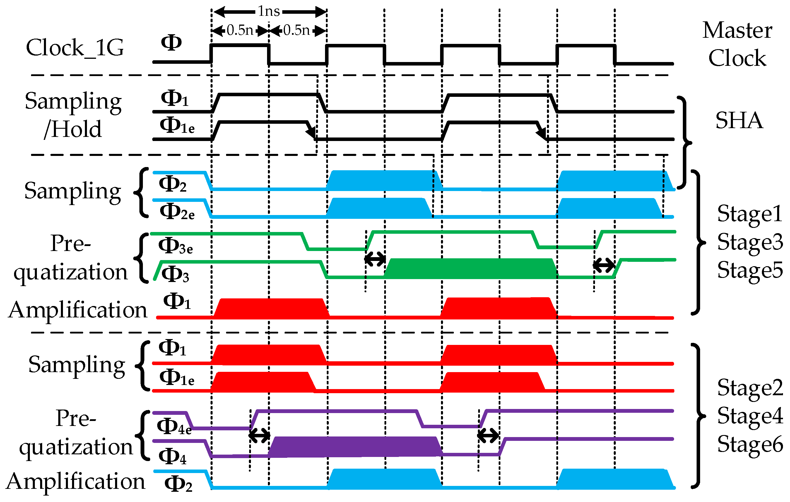
2.2.2. Pre-Quantization Timing

PQT, including sampling, pre-quantization, and amplification phases, is presented in Figure 3. Compared with traditional timing, Ф1, Ф1e, Ф2, and Ф2e are the same for both timing strategies. Different from traditional timing, pre-quantization is introduced to comparators. PQT focuses on the distribution of timing, which aims to optimize the sample and quantizationtiming, thus maximizing the amplifier’s settling time. By dividing half of the sampling phase to the comparator, PQT strategy can relieve the pressure on the operational amplifier’s output-setting. During the sampling phase, the Ф3e resets the comparator output to a high-level 100 ps early, and then the comparator works normally during 25% of the duty cycle of Ф3. The whole quantization is completed within about 250 ps.
  • Sampling: The period of Ф1 or Ф2 is double to that of Ф; when Ф1 or Ф2 are sampling clock signal, it is the square wave signal that controls the switched capacitor circuit to start sampling.
  • The bottom plate sampling: Ф1e and Ф2e are early shut-down clocks; the falling edge of Ф1 is earlier than that of Ф1e, and the falling edge of Ф2e is earlier than that of Ф2, which are used to ensure the bottom plate sampling technology;
  • Pre-quantization: Ф3 and Ф4 are clocks for the comparator. The high voltages of Ф3 and Ф4 are at the half voltages of Ф2 or Ф1, respectively. The comparator occupies about 250 ps of time to complete quantization. During the phases of Ф3 and Ф4, comparators reset the output to a high voltage 100 ps early.
  • Amplification: clock for amplification. Ф1 is the non-overlapping clock signal of Ф22 is the non-overlapping clock signal of Ф1), used to control the op-amp to start amplifying at the high level.

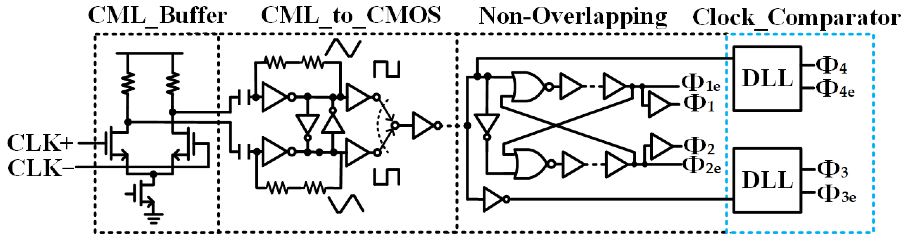
2.2.3. Clock Generation Circuit of PQT

As PQT pointed out in Section 2.2.2, the 1 GSps 12-bit ADC must generate the timing: Ф1, Ф1e, Ф2, Ф2e, Ф3, Ф3e, Ф4, and Ф4e.
The clock generation circuit is shown in Figure 4. The high-speed data interface uses current-mode logic (CML) as the receiving end of the clock, and then converts the output voltage of the CML to the CMOS logic voltage. In the non-overlapping schematic, the timing can be improved by adding more buffers. A clock with a 50% duty cycle is provided for SHA and MDACs with a frequency of 1 GHz. A comparator requires a clock with a duty cycle of 25%, which is common in time-domain interleaving mode based on an external frequency of a 2-GHz clock. In this ADC, DLL (blue frame) is applied to generate the clock of the comparator, solving the problem of two master clocks.

3. Circuit Implementation and Calibration

3.1. DLL in Clock Generation Circuit

The delay lock loop is composed of a variable delay line (VDL), phase frequency detector (PFD), a charge pump, and a mux module (CLK_CMP_MUX), shown in Figure 5a. The delay lock loop is mainly used to generate an accurate delay time, and this delay does not change with external conditions such as temperature and voltage changes.
The basic unit of VDL is shown in Figure 5b. It is composed of a basic inverter and a control terminal Vct. Increasing the load can increase the delay time of timing, but it will also slow down the rising and falling edges [25]. Therefore, Vct needs to be properly controlled by a charge pump. Multiple (even 4/8/16) basic units can be used to increase the overall delay. In order to adapt to the clock frequency of 1.25 GHz~250 MHz, four same cell delay lines can be selected by control code P/N<0:2>. Adjusting the voltage of Vct can make the rising edge of each delay line unit steeper or flatter, so as to achieve the purpose of adjusting the delay of the entire VDL. Considering the adjustment capability of each VDL, when the clock frequency is low, multiple groups of the same VDL can be used in series to increase the overall delay, and the number of VDLs in series is controlled by P/N<0:2>. For example, delay line1 is selected in Figure 5c. The timing of the delay line is introduced. A clock CLKC with a 25% duty cycle can be obtained through the simple logic operation of CKA and CKC. CKA is delayed by 25% more of the clock cycle than CK. It is difficult to directly generate CKA through CK, but it is easy to delay CK by 50% of the clock cycle to obtain CKB due to CK and CKB being inverse. CKB and CKC are also inversely related. The phase detector detects the relationship between CK and CKC. If the delay in CKC is too large, the charge pump makes the Vct smaller. Otherwise, it makes the Vct larger until the delay of VDL is exactly equal to one clock cycle. At this time, the final output of the DLL is CLKC.

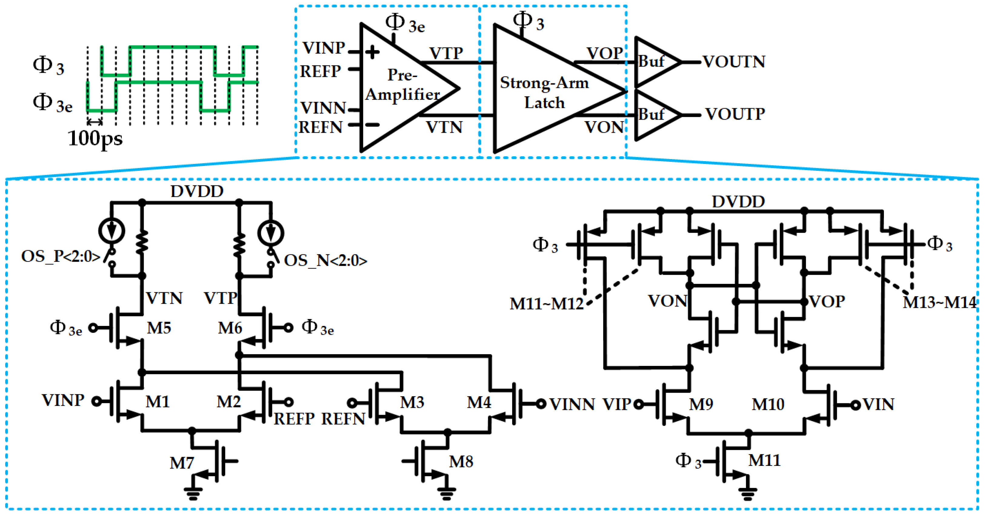
3.2. Four-Port Comparator in Sub-ADCs

The comparator is one of the most commonly used modules in the sub-ADCs. As shown in Figure 6, a four-port comparator consists of pre-amplifier, latch, buffer, and calibration circuit. In this design, the pre-amplifier isolates the kick-back noise generated by the strong-arm latch. The strong-arm latch with cross-coupled pairs is used to directly produce the rail-to-rail outputs for the output signal of the pre-amplifier [26]. Based on the mentioned clocks Ф3 and Ф3e in Section 2, the timing of comparator is divided into two phases. In the first phase of Ф3e, Ф3 is at a low level. Transistor M9 and M10 are off, while transistors M11–M14 as switches are on. Then, the output terminals VOP and VON are pulled up to DVDD. The process of resetting the comparator is finished. At the same time, the MOSFETs do not work, so there is no static power consumption. In the second phase of Ф3, Ф3 is at a high level. VIP and VIN are the two differential signal inputs, coming from the output of the pre-amplifier. The input signals realize signal conversion through the cross-coupled pairs, which can quickly increase the current of the circuit and cause VOP and VON to become high- or low-voltage.
The offset of the comparator mainly comes from differential pairs M1–M4 and M9–M10, which cannot go beyond 1/2 LSB of this sub-ADC, otherwise the residual will exceed the quantification range of the next stage. In this design, the equivalent input offset voltage (VOS) of the comparator is about ±53 mV within the 3-sigma interval of the Monte Carlo simulation. The offset contributed by the pre-amplifier is about ±36 mV, more than the offset of the latch. To decrease the offset, the sizes of M1 and M2 are increased to match better, and the overdrive voltage of the input MOSFET is reduced to 105 mV.
To correct the offset, a 3-bit calibration circuit is added in the pre-amplifier to correct the offset of the comparator by controlling OS_P<2:0>and OS_N<2:0> in Figure 7a. A detailed calibration process for offset is mentioned in Section 3.5.1. Figure 7b is the equivalent circuit of Figure 7a.
As is shown in Figure 7a, the offset and output common mode are changed when ΔI is introduced. When ignoring channel length modulation effect and ΔI ≠ 0, the relationship between VOS and ΔI is as Equation (1):
V OS = 2 I Δ I u n C ox W L 2 I + Δ I u n C ox W L
As is shown in Figure 7b, an additional VOS is caused by ΔI at the input. VTP’ and VTN’ are the output ports. When ΔI ≠ 0, the output common mode is increased as in Equation (2):
VTP VTP = VTN VTN = Δ I 2 × R

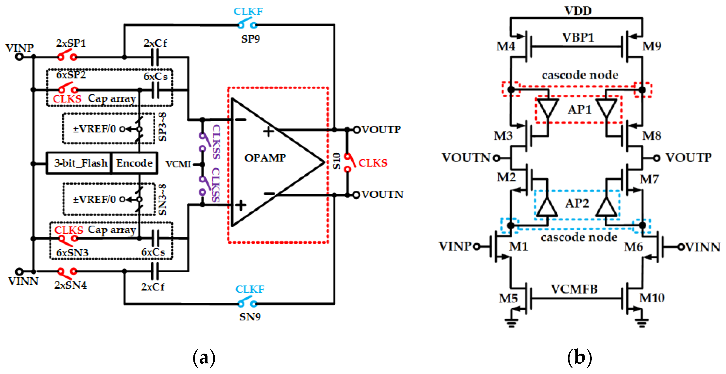
3.3. Flip-Around Sample and Hold Amplifier (SHA)

The pipelined ADC can be divided into two categories: SHA-less pipelined ADC and pipelined ADC with SHA [27,28,29,30]. SHA is placed ahead of MDAC in comparison to SHA-less ADC for several reasons. Firstly, because a comparator cannot compare a changing signal, SHA is used to obtain an unchanged sampled signal, especially for IF sampling applications. Secondly, although SHA brings extra power consumption and nonlinearity to some extent, the performance of sample and hold amplify (SHA) is relatively stable in the full frequency band.
The topology of flip-around SHA is shown in Figure 8a. Compared with non-flip-around SHA, this structure has a small area, low noise, and low power consumption due to its one capacitor and large feedback coefficient. In this design, the technology of bottom-plate sampling is selected. VGSS (Ф1e) is turned off before VGS (Ф1), which reduces the influence of charge injection on the sampling MOSFETs M1 and M2. In addition, the clock feed-through of the gate-drain and gate-source flipped capacitors can be eliminated through this technique; otherwise, there will be errors in the sampling output voltage. Dummy MOSFETs are also added to the symmetrical structure to reduce the impact of charge injection further. According to the conservation of charge at the sampling and hold phase phases, the transfer function of SHA can be shown as Equation (3):
VOUT = VOUTP VOUTN = 1 1 + 1 A ( VINP VINN )
Due to the gain (A) of operational amplifier being ∞, the ideal the transfer function of SHA can be shown as Equation (4):
VOUT A = VIN
Because of the limited gain (A) of the operational amplifier and the required accuracy of 12 bits, the error of VOUT under the maximum amplitude of one side (0.6 V) needs to satisfy the Equation (5):
VOUT error = | VOUT VOUT A | < 1 2 × 2 12
Considering the parasitic effect of layout, the DC gain selected is 75 dB. The high-gain operational amplifier is introduced in Section 3.4.
In Figure 8b, a bootstrapped switch is utilized for sampling, whose on-resistance is smaller than that of the MOS or CMOS switch, helping SHA obtain a higher linearity and faster speed. During the sampling phase, CLKN (red arrow) changes from DVDD to DVSS. M7, M8, and M4 turn on. The parasitic capacitance CP of the node VG results in the sampled signal generating input-related nonlinearity because the gate source voltage of M3 is less than VDD and is related to the input voltage VIN. The relationship between VG and VIN is shown in Equation (6):
V G = CB CB + CP VDD CB CB + CP V IN
M9 and M3 use Deep-Nwell (DNW) MOSFETs to decrease the effect of channel length modulation. M7 is applied to prevent the risk of breakdown in M5. During the hold phase (blue arrow), CLKN changes from DVSS to DVDD. M1, M2, and M6 turn on. CB begins to charge, while VG discharges to zero potential through M5 and M6.

3.4. Operational Amplifier (Op-Amp) in the SHA or MDACs

Figure 9a depicts a fully differential 2.5-bit flip-around MDAC. In the flip-around MDAC schematic, capacitors (Cs and Cf) are used for the sampling phase and the feedback phase, respectively. Cap arrays are composed of capacitors and switches (6 × Cs, 6 × SP2, 6 × SN2). Switch S10 can guarantee that the beginning of output settling is common-mode voltage 0.9 V, decreasing the error of output to some extent. In the sampling phase, switches (2 × SP1, 6 × SP2, 6 × SN3, 2 × SN4) turn on. Switch S10 also turns on. At the same time, 3-bit flash, which includes six comparators, obtains the result of the comparison by comparing VIN with VREF. In the feedback phase, switches (SP9, SN9) turn on, and the operational amplifier operates normally.
A higher gain operational amplifier with a telescope cascode configuration is used in flip-around SHA or MDACs, as is shown in Figure 8b and Figure 9b. Its advantages are high single-stage gain and current efficiency, relatively low noise, and greater stability compared with multistage operational amplifiers. When CLKF is at a high voltage, the operational amplifier of MDAC1 operates normally. Both the NMOS and PMOS sides are cascaded. AP1 and AP2 are the gains of auxiliary op-amps. The gain of this operational amplifier is described by Equation (7):
A = g m 6 × { ( 1 + AP 2 ) × g m 7 r o 7 r o 6 } { ( 1 + AP 1 ) × g m 8 r o 8 r 09 }  
Gm6, gm7, and gm8 are transconductances of M6, M7, and M8, respectively. Ro6, ro7, ro8, and ro9 are the resistance of M6, M7, and M8, respectively. Simulation results show that the gain of this op-amp is about 78 dB. GBW is about 13.5 GHz.

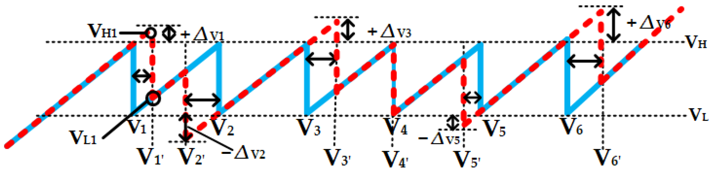
3.5. Calibration of Mismatches and Errors

As is shown in Table 1, this ADC adopts the following calibration strategies to reduce the sensitivity to mismatches and errors. The digital domain calibration technology of this paper adopts the following three methods: adjustable current source, Efuse combined with multi-target search, and pseudo-random noise injection. The inter-stage gain is affected not only by the finite open-loop gain of the operational amplifier but also by the capacitor mismatch error [31]. Since precise sub-DAC is the premise of correct background calibration, it is necessary to calibrate the DAC error caused by capacitor mismatch before background calibrations.
In this design, the capacitor mismatch should be corrected first through the foreground calibration, followed by the background calibration to rectify the inter-stage gain errors.

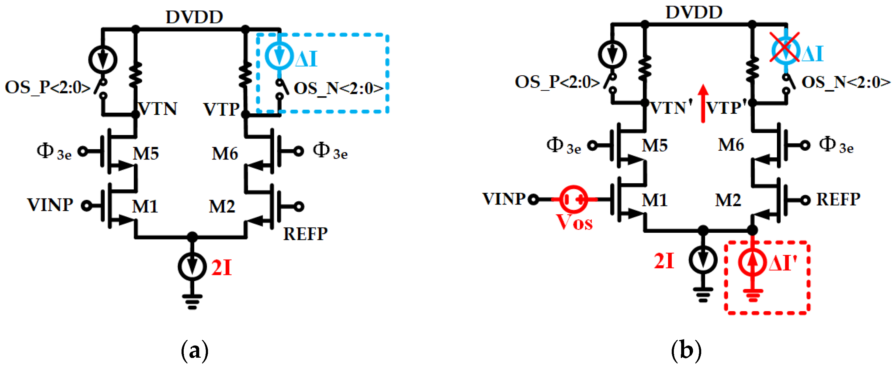
3.5.1. Calibration of Offset Voltage

The offset voltage of the comparator is mainly caused by the mismatch of differential pairs. If there is a deviation in the comparator threshold, the output residual voltage exceeds the quantization range of the next stage, resulting in the loss of signal-related information and missing codes. For the 2.5-bit pipeline stage, the sub-ADC is a flash ADC with six comparators. The comparison reference voltages of these six comparators are ±5/8 Vref, ±3/8 Vref, and ±1/8 Vref. Each of the six comparators with different thresholds needs to be calibrated. There are several ways to calibrate the offset of the comparator in the analog domain:
  • The first method is to add an adjustable capacitor to the output of the comparator. However, this method increases the load on the circuit and affects the switching speed of the comparator [32];
  • The second option is to reduce the input offset of the comparator by adjusting the substrate voltage. However, separating the substrates of MOSFETs in a CMOS process requires the use of special deep-well devices [11];
  • The third way is to calibrate the offset of the comparator through the auxiliary differential pair. By adding auxiliary differential pairs, this solution inevitably increases the noise of the comparator [33];
  • In theory, adding an adjustable current source can adjust the offset of the comparator [34]. As can be seen from Section 3.3, bias current is placed in the output of the preamplifier in this design. The advantages of this method are low noise and ease in matching the calibration of the residual curve.
As is shown in Figure 10, a 3-bit calibration circuit is added to the output end of the pre-amplifier. Since the equivalent input offset voltage (VOS) of the comparator is about ±52 mV within the 3-sigma interval of the Monte Carlo simulation, the step of adjustment 8 mV is reasonable, which can cover about ±56 mV offset voltage.

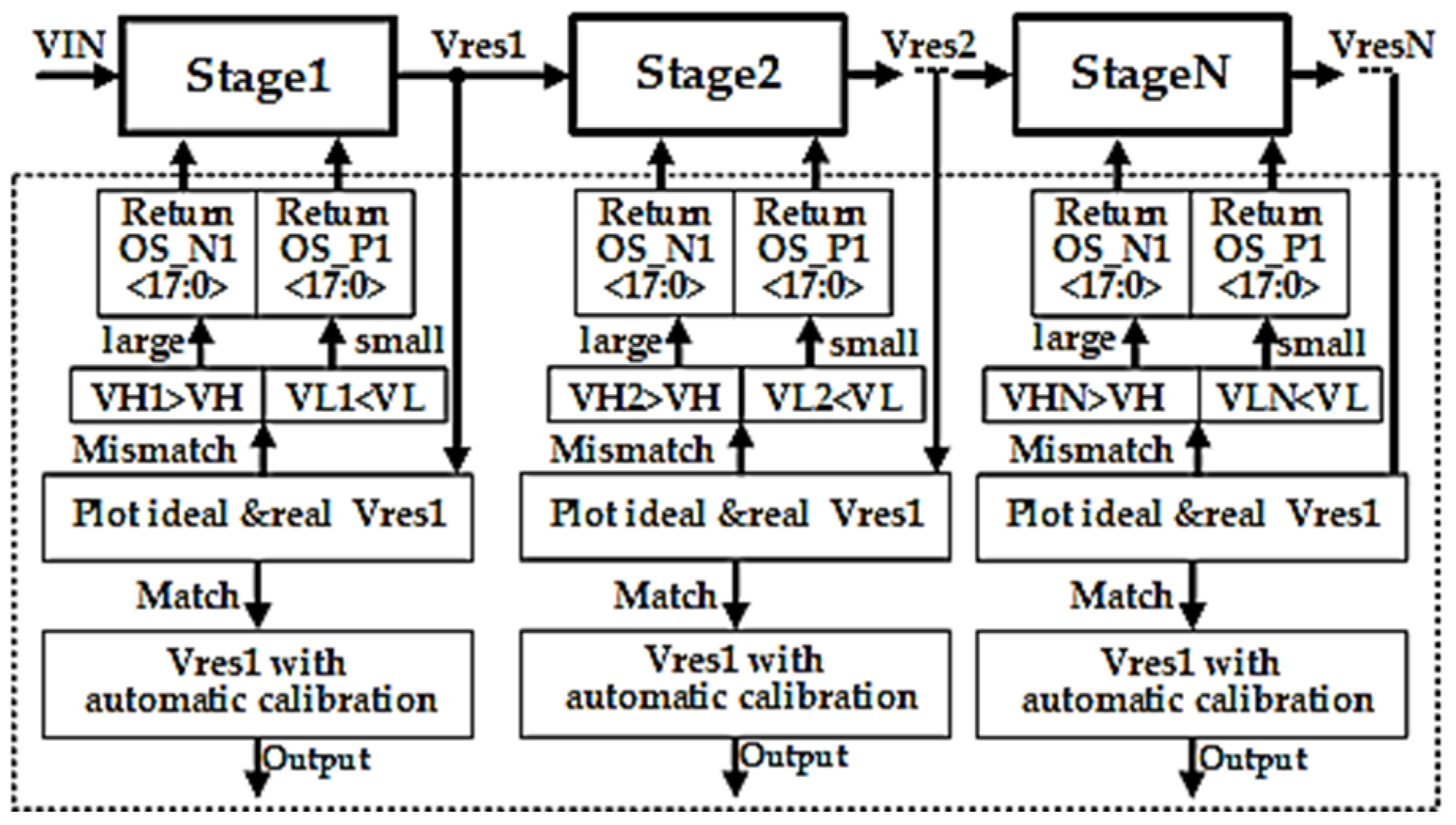
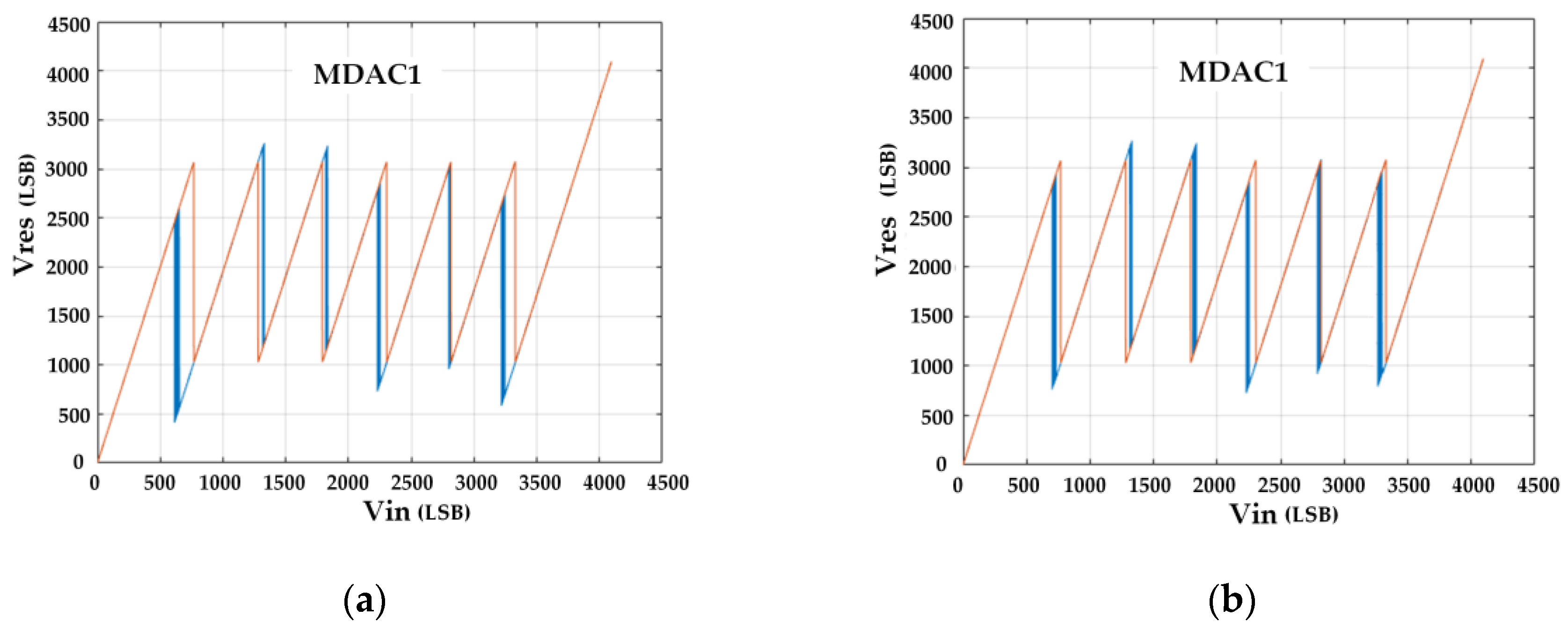
3.5.2. Automatic Calibration of Residual Curves

Automatic calibration of residual curves is proposed in Figure 11. The residual curve of each MDAC is calibrated by the method of plotting the residual curve. As is shown in Figure 12, the red line in the figure is the ideal residual curve, which is uniformly distributed near the threshold values V1–V6. The range of Vres is the difference between the maximum VH and minimum VL. The blue line is a non-ideal residual curve. The distribution of the residual curve obviously exceeds the range of VH and VL due to the imbalance of the threshold values ΔV1, ΔV2, ΔV3, ΔV4, ΔV5, and ΔV6 series of deviations in V6. As shown in Figure 7, the comparator offset of the ADC can be corrected by adjusting the bias current of the preamplifier. In order to avoid the complexity of calibration and improve efficiency, this algorithm mainly conducts an automatic calibration on the output curve of each stage of the pipeline on chip from the perspective of automatic calibration.
The offset voltage of the comparator is mainly caused by the mismatch of differential pairs. As shown in Figure 12, the flow chart of automatic calibration is presented. After each stage of the pipeline outputs the residual curve, it performs the following automatic calibration steps.
First, it draws the residual curve VresN and the ideal curve VresN0. The maximum and minimum values of the residual curve are VL and VH, respectively.
The automatic calibration calculation process involves judging whether the range of the residual curve exceeds the maximum and minimum values of the ideal curve, getting the maximum and minimum values of the residual curve near each threshold V1′–V6′. If V1′ > V1, the maximum value VH + ΔV1 is saved, which exceeds (VL, VH). If V2′ < V2, the minimum value VH–ΔV1 that exceeds (VL, VH) is saved. When the maximum and minimum values of the residual curve exceed the range (VL and VH), the control code OS_N or OS_P adjusts the bias current of the preamplifier to correct the comparator threshold offset.
During the working time of the ADC, control code OS_N or OS_P is continuously sent to the register on chip via the SPI interface until the minimum value of V is found, at which point the automatic calibration is considered complete.
Outputs of Vres after automatic calibration, as shown in Figure 13. Before calibrating the Vres of MDAC1, the first and sixth thresholds deviate from the ideal thresholds severely. After calibration, the Vres of MDAC1 is closer to the ideal Vres. The method of automatic calibration by plotting a residual curve to calibrate the residual curve is effective.

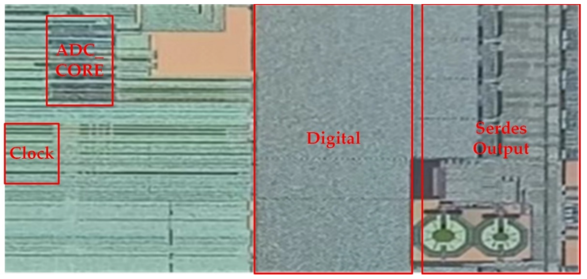
4. Measured Results and Discussion

The chip manufactured in a 40 nm CMOS process occupies an area of 2.16 mm2. The layout of ADC_CORE is shown in Figure 14, including the input buffer, SHA, and Stage1–6. The die micrograph is shown in Figure 15, including ADC_CORE, digital correction, and serdes output. Many decoupling capacitors are filled in the spare spaces between different blocks to keep the power supply voltage clean and stable.
The static performance of DNL and INL is presented in Figure 16. 65,536 sample points are saved to calculate DNL and INL. The measured DNL and INL are −0.72/+0.68 LSB and −1.52/+1.51 LSB after calibration, respectively. Figure 17 shows a fast Fourier transform (FFT) plot of the ADC output before and after calibration at the input frequency of 227 MHz and 1 GSps. Figure 18 shows the SFDR and SNR of this ADC versus the frequency of the input signal with and without calibration at 1 GS/s. For example, this ADC can achieve an SNR of 57.38 dB and an SFDR of 78.5 dB with 227 MHz input frequency. The SFDR can be greatly improved when the input frequency is low.
Table 2 summarizes the comparison of this work with previous published papers for ADCs with higher than 10-bit resolution or faster than 80 MS/s. Our work shows a relatively good SFDR and SNR under the acceptable FoM with the help of the proposed timing. The power consumption of this ADC is higher than its counterparts in Table 2, and the performance of our work is relatively better, so the FoM of this ADC is not the lowest. SHA-less architecture and new open-loop op-amp can be researched to reduce power consumption in the future. The 10-bit, 80 MS/s pipelined ADC achieves the bit error rate of 10−15 errors/sample, which is a factor between 104 to 106 less than in a comparable lookahead pipelined ADC [35]. Our work can achieve the same BER level at higher speed and accuracy.

5. Conclusions

In this paper, a 12-bit 1 GS/s pipelined ADC was developed, which was manufactured in a 40 nm CMOS process. The reasonable and improved working timing is provided to maximize the output-settling time of operational amplifier, which can make the op-amp output more complete. The clock generation circuit, along with DLL, is explored to generate accurate a duty of timing for each stage, which can avoid the 2-GHz external clock mentioned by previous studies on pipelined ADCs. Based on PQT, a four-port comparator is adopted for this ADC to obtain a bit error rate below 10−15, less than that in a comparable lookahead pipelined ADC. The offset of the comparator is analyzed by equations and simulated by the Monte Carlo simulation. For calibration strategies to reduce the sensitivity to mismatches and errors, automatic calibration of the residual curve is explored, which can effectively to correct residual curve. Finally, this ADC is tested and measured to obtain relatively good performance. It exhibits an SNDR of 57.3 dB and an SFDR of 78.54 dB for a 227 MHz input signal at 1 GS/s under the acceptable FoM with the help of the proposed timing.

Author Contributions

Conceptualization, F.X., Z.L. and X.G.; methodology, F.X., Z.L. and X.G.; software, F.X., H.J. and X.G.; validation, F.X., X.G. and H.J.; formal analysis, F.X. and Z.L.; investigation, F.X. and X.G.; resources, D.W. and J.W.; data curation, H.J.; writing—original draft preparation, F.X.; writing—review and editing, H.J., J.W. and X.G.; visualization, D.W.; supervision, J.W. and D.W.; project administration, J.W. and D.W.; funding acquisition, D.W. All authors have read and agreed to the published version of the manuscript.

Funding

This research was funded by the “Strategic Priority Research Program” of the Chinese Academy of Sciences (Grant XDC07020400).

Conflicts of Interest

The authors declare no conflict of interest.

References

  1. Niu, H.; Yuan, J. A Spectral-Correlation-Based Blind Calibration Method for Time-Interleaved ADCs. IEEE Trans. Circuits Syst. I Regul. Pap. 2020, 67, 5007–5017. [Google Scholar] [CrossRef]
  2. Jiang, W.; Zhu, Y.; Zhang, M.; Chan, C.H.; Martins, R.P. A Temperature-Stabilized Single-Channel 1-GS/s 60-dB SNDR SAR-Assisted Pipelined ADC with Dynamic Gm-R-Based Amplifier. IEEE J. Solid-State Circuits 2020, 55, 322–332. [Google Scholar] [CrossRef]
  3. Ramkaj, A.T.; Ramos, J.C.P.; Pelgrom, M.J.M.; Steyaert, M.S.J.; Verhelst, M.; Tavernier, F. A 5-GS/s 158.6-mW 9.4-ENOB Passive-Sampling Time-Interleaved Three-Stage Pipelined-SAR ADC with Analog–Digital Corrections in 28-nm CMOS. IEEE J. Solid-State Circuits 2020, 55, 1553–1564. [Google Scholar] [CrossRef]
  4. Wu, C.; Yuan, J. A 12-Bit, 300-MS/s Single-Channel Pipelined-SAR ADC With an Open-Loop MDAC. IEEE J. Solid-State Circuits 2019, 54, 1446–1454. [Google Scholar] [CrossRef]
  5. Guangming, Y.; Sansen, W. A high-frequency and high-resolution fourth-order /spl Sigma//spl Delta/ A/D converter in BiCMOS technology. IEEE J. Solid-State Circuits 1994, 29, 857–865. [Google Scholar] [CrossRef]
  6. Walden, R.H. Analog-to-digital converter survey and analysis. IEEE J. Sel. Areas Commun. 1999, 17, 539–550. [Google Scholar] [CrossRef]
  7. Li, J.; Guo, X.; Luan, J.; Wu, D.; Zhou, L.; Huang, Y.; Wu, N.; Jia, H.; Zheng, X.; Wu, J.; et al. A 3GSps 12-bit four-channel time-interleaved pipelined ADC in 40 nm CMOS process. Electronics 2019, 8, 1551. [Google Scholar] [CrossRef]
  8. Bae, C.; Shin, S.; Jung, J.; Park, M.; Kwon, K.; Kim, J.; Jung, T.; Choi, J. An 11-bit Ring Amplifier Pipeline ADC with Settling-Time Improvement Scheme. In Proceedings of the 2020 International Conference on Electronics, Information, and Communication (ICEIC), Shenzhen, China, 19–22 January 2020; pp. 1–4. [Google Scholar]
  9. Hershberg, B.; Dermit, D.; Liempd, B.; Martens, E.; Markulic, N.; Lagos, J.; Craninckx, J. 3.1 A 3.2GS/s 10 ENOB 61mW Ringamp ADC in 16 nm with Background Monitoring of Distortion. In Proceedings of the 2019 IEEE International Solid-State Circuits Conference—(ISSCC), San Francisco, CA, USA, 17–21 February 2019; pp. 58–60. [Google Scholar]
  10. Louwsma, S.M.; Tuijl, A.J.M.; Vertregt, M.; Nauta, B. A 1.35 GS/s, 10 b, 175 mW Time-Interleaved AD Converter in 0.13 µm CMOS. IEEE J. Solid-State Circuits 2008, 43, 778–786. [Google Scholar] [CrossRef]
  11. Zheng, X.; Wang, Z.; Li, F.; Zhao, F.; Yue, S.; Zhang, C.; Wang, Z. A 14-bit 250 MS/s IF Sampling Pipelined ADC in 180 nm CMOS Process. IEEE Trans. Circuits Syst. I Regul. Pap. 2016, 63, 1381–1392. [Google Scholar] [CrossRef]
  12. Carnes, J.; Un-Ku, M. The Effect of Switch Resistance on Pipelined ADC MDAC Settling Time. In Proceedings of the 2006 IEEE International Symposium on Circuits and Systems (ISCAS), Island of Kos, Greece, 21–24 May 2006; p. 4. [Google Scholar]
  13. Li, F.; Wang, Z.; Li, D. An Incomplete Settling Technique for Pipelined Analog-to-Digital Converters. In Proceedings of the 2007 IEEE International Symposium on Circuits and Systems, New Orleans, LA, USA, 27–30 May 2007; pp. 3590–3593. [Google Scholar]
  14. Zhang, M.; Zhu, Y.; Chan, C.H.; Martins, R.P. An 8-Bit 10-GS/s 16× Interpolation-Based Time-Domain ADC with <1.5-ps Uncalibrated Quantization Steps. IEEE J. Solid-State Circuits 2020, 55, 3225–3235. [Google Scholar]
  15. Zhu, S.; Wu, B.; Cai, Y.; Chiu, Y. A 2-GS/s 8-bit Non-Interleaved Time-Domain Flash ADC Based on Remainder Number System in 65-nm CMOS. IEEE J. Solid-State Circuits 2018, 53, 1172–1183. [Google Scholar] [CrossRef]
  16. Sahoo, B.D.; Razavi, B. A 10-b 1-GHz 33-mW CMOS ADC. IEEE J. Solid-State Circuits 2013, 48, 1442–1452. [Google Scholar] [CrossRef]
  17. Kratyuk, V.; Hanumolu, P.K.; Ok, K.; Moon, U.K.; Mayaram, K. A Digital PLL with a Stochastic Time-to-Digital Converter. IEEE Trans. Circuits Syst. I Regul. Pap. 2009, 56, 1612–1621. [Google Scholar] [CrossRef]
  18. Xu, H.; Abidi, A.A. Analysis and Design of Regenerative Comparators for Low Offset and Noise. IEEE Trans. Circuits Syst. I Regul. Pap. 2019, 66, 2817–2830. [Google Scholar] [CrossRef]
  19. Ali, A.M.A.; Dillon, C.; Sneed, R.; Morgan, A.S.; Bardsley, S.; Kornblum, J.; Wu, L. A 14-bit 125 MS/s IF/RF Sampling Pipelined ADC with 100 dB SFDR and 50 fs Jitter. IEEE J. Solid-State Circuits 2006, 41, 1846–1855. [Google Scholar] [CrossRef]
  20. Li, J.; Zeng, X.; Xie, L.; Chen, J.; Zhang, J.; Guo, Y. A 1.8-V 22-mW 10-bit 30-MS/s Pipelined CMOS ADC for Low-Power Subsampling Applications. IEEE J. Solid-State Circuits 2008, 43, 321–329. [Google Scholar] [CrossRef]
  21. Yang, P.; Wang, X.; Wang, C.; Li, F.; Jiang, H.; Wang, Z. A 14-bit 200-Ms/s SHA-Less Pipelined ADC with Aperture Error Reduction. IEEE Trans. Very Large Scale Integr. (VLSI) Syst. 2020, 28, 2004–2013. [Google Scholar] [CrossRef]
  22. Naderi, M.H.; Silva-Martinez, J. Algorithmic-Pipelined ADC with a Modified Residue Curve for Better Linearity. In Proceedings of the 2017 IEEE 60th International Midwest Symposium on Circuits and Systems (MWSCAS), Boston, MA, USA, 6–9 August 2017; pp. 1446–1449. [Google Scholar]
  23. Lee, Z.M.; Wang, C.Y.; Wu, J.T. A CMOS 15-bit 125-MS/s Time-Interleaved ADC with Digital Background Calibration. IEEE J. Solid-State Circuits 2007, 42, 2149–2160. [Google Scholar] [CrossRef]
  24. Cao, Y.; Zhang, S.; Zhang, T.; Chen, Y.; Zhao, Y.; Chen, C.; Ye, F.; Ren, J. A 91.0-dB SFDR Single-Coarse Dual-Fine Pipelined-SAR ADC with Split-Based Background Calibration in 28-nm CMOS. IEEE Trans. Circuits Syst. I Regul. Pap. 2021, 68, 641–654. [Google Scholar] [CrossRef]
  25. Jia, H.; Guo, X.; Wu, D.; Zhou, L.; Luan, J.; Wu, N.; Huang, Y.; Zheng, X.; Wu, J.; Liu, X. A 12-Bit 2.4 GS/s Four-Channel Pipelined ADC with a Novel On-Chip Timing Mismatch Calibration. Electronics 2020, 9, 910. [Google Scholar] [CrossRef]
  26. Jithin, G.; Prasad, G.B.V.S.V.; Krishna, J.V.N.S.; Pande, K.S. Strong Single-Arm Latch Comparator with Reduced Power Consumption. In Proceedings of the 2021 Fourth International Conference on Electrical, Computer and Communication Technologies (ICECCT), Erode, India, 15–17 September 2021; pp. 1–6. [Google Scholar]
  27. Brandolini, M.; Shin, Y.J.; Raviprakash, K.; Wang, T.; Wu, R.; Geddada, H.M.; Ko, Y.J.; Ding, Y.; Huang, C.S.; Shih, W.T.; et al. A 5 GS/s 150 mW 10 b SHA-Less Pipelined/SAR Hybrid ADC for Direct-Sampling Systems in 28 nm CMOS. IEEE J. Solid-State Circuits 2015, 50, 2922–2934. [Google Scholar] [CrossRef]
  28. Devarajan, S.; Singer, L.; Kelly, D.; Pan, T.; Silva, J.; Brunsilius, J.; Rey-Losada, D.; Murden, F.; Speir, C.; Bray, J.; et al. A 12-b 10-GS/s Interleaved Pipeline ADC in 28-nm CMOS Technology. IEEE J. Solid-State Circuits 2017, 52, 3204–3218. [Google Scholar] [CrossRef]
  29. Zhu, C.; Lin, J.; Wang, Z. Background Calibration of Comparator Offsets in SHA-Less Pipelined ADCs. IEEE Trans. Circuits Syst. II Express Briefs 2019, 66, 357–361. [Google Scholar] [CrossRef]
  30. Huang, P.; Hsien, S.; Lu, V.; Wan, P.; Lee, S.C.; Liu, W.; Chen, B.W.; Lee, Y.P.; Chen, W.T.; Yang, T.Y.; et al. SHA-Less Pipelined ADC with In Situ Background Clock-Skew Calibration. IEEE J. Solid-State Circuits 2011, 46, 1893–1903. [Google Scholar] [CrossRef]
  31. Chuang, S.Y.; Sculley, T.L. A digitally self-calibrating 14-bit 10-MHz CMOS pipelined A/D converter. IEEE J. Solid-State Circuits 2002, 37, 674–683. [Google Scholar] [CrossRef]
  32. Chan, C.H.; Zhu, Y.; Chio, U.F.; Sin, S.W.; Seng-Pan, U.; Martins, R.P. A Voltage-Controlled Capacitance Offset Calibration Technique for High Resolution Dynamic Comparator. In Proceedings of the 2009 International SoC Design Conference (ISOCC), Busan, Republic of Korea, 22–24 November 2009; pp. 392–395. [Google Scholar]
  33. Atherton, J.H.; Simmonds, H.T. An offset reduction technique for use with CMOS integrated comparators and amplifiers. IEEE J. Solid-State Circuits 1992, 27, 1168–1175. [Google Scholar] [CrossRef]
  34. Katyal, V.; Geiger, R.L.; Chen, D.J. A New High Precision Low Offset Dynamic Comparator for High Resolution High Speed ADCs. In Proceedings of the 2006 IEEE Asia Pacific Conference on Circuits and Systems, Singapore, 4–7 December 2006; pp. 5–8. [Google Scholar]
  35. Guhados, S.; Hurst, P.J.; Lewis, S.H. A Pipelined ADC with Metastability Error Rate <10−15 Errors/Sample. IEEE J. Solid-State Circuits 2012, 47, 2119–2128. [Google Scholar]
  36. Lagos, J.; Hershberg, B.; Martens, E.; Wambacq, P.; Craninckx, J. A 1Gsps, 12-bit, Single-Channel Pipelined ADC with Dead-Zone-Degenerated Ring Amplifiers. In Proceedings of the 2018 IEEE Custom Integrated Circuits Conference (CICC), San Diego, CA, USA, 8–11 April 2018; pp. 1–4. [Google Scholar]
  37. Naderi, M.H.; Park, C.; Prakash, S.; Kinyua, M.; Soenen, E.G.; Silva-Martinez, J. A 27.7 fJ/conv-step 500 MS/s 12-Bit Pipelined ADC Employing a Sub-ADC Forecasting Technique and Low-Power Class AB Slew Boosted Amplifiers. IEEE Trans. Circuits Syst. I Regul. Pap. 2019, 66, 3352–3364. [Google Scholar] [CrossRef]
  38. Moon, K.J.; Oh, D.R.; Choi, M.; Ryu, S.T. A 28-nm CMOS 12-Bit 250-MS/s Voltage-Current-Time Domain 3-Stage Pipelined ADC. IEEE Trans. Circuits Syst. II Express Briefs 2020, 67, 2843–2847. [Google Scholar] [CrossRef]
  39. Hung, T.C.; Liao, F.W.; Kuo, T.H. A 12-Bit Time-Interleaved 400-MS/s Pipelined ADC with Split-ADC Digital Background Calibration in 4,000 Conversions/Channel. IEEE Trans. Circuits Syst. II Express Briefs 2019, 66, 1810–1814. [Google Scholar] [CrossRef]
Figure 1. Block diagram of 1 GS/s 12-bit pipelined analog-to-digital converter (ADC). The proposed pre-quantization timing, including Ф1, Ф1e, Ф2, Ф2e, Ф3, Ф3e, Ф4, and Ф4e, is generated by a clock schematic. The clock schematic comprises a high-speed interface current mode logic (CML), a non-overlapping clock, and a DLL.
Electronics 12 00924 g001
Figure 2. The traditional timing, including the sampling phase and the amplification phase. Detailed timing is provided for SHA, Stage1~Stage6. Ф1, Ф1e, and Ф2 are provided for Stage1, Stage3, and Stage5 to sample and amplify. Ф2, Ф2e, and Ф1 are provided for Stage2, Stage4, and Stage6 to sample and amplify. The green and purple parts represent quantization.
Electronics 12 00924 g002
Figure 3. Pre-quantization timing, including sampling, pre-quantization, and amplification phase. Detailed timing is provided for SHA, Stage1~Stage6. For Stage1, Stage3 and Stage5, Ф1, Ф1e, and Ф2 are provided to sample and amplify. For Stage2, Stage4, and Stage6, Ф3 and Ф3e are designed for comparators. Ф2, Ф2e, and Ф1 are provided to sample and amplify. Ф4 and Ф4e are designed for comparators.
Electronics 12 00924 g003
Figure 4. Clock schematic, including current mode logic, CML to the CMOS logic voltage, and non-overlapping with the outputs Ф1, Ф1e, Ф2, and Ф2e. DLL is added to generate Ф3, Ф3e, Ф4, and Ф4e.
Electronics 12 00924 g004
Figure 5. Delay lock loop. (a) Delay lock loop schematic; (b) Delay line schematic; (c) timing of delay line.
Electronics 12 00924 g005
Figure 6. Comparator schematic, including pre-amplifier, strong-arm latch, and buffer. Ф4 and Ф4e are clocks for the designed comparators.
Electronics 12 00924 g006
Figure 7. (a) Pre-amplifier with calibration. (b) Equivalent circuit (a). VOS and raised output common mode caused by ΔI.
Electronics 12 00924 g007
Figure 8. (a) Flip-around SHA schematic. (b) Bootstrapped switches, used in the SHA and MDACs.
Electronics 12 00924 g008
Figure 9. (a) A fully differential 2.5-bit flip-around MDAC. The operational amplifier gain is equal to 4. The sampling switch is bootstrapped. (b) Operational amplifier schematic. Both the NMOS and PMOS sides are cascaded. AP1 and AP2 are auxiliary op-amps, added to improve gain.
Electronics 12 00924 g009
Figure 10. Monte Carlo simulation of the comparator, showing the offset voltage of comparator.
Electronics 12 00924 g010
Figure 11. Automatic calibration of residual curves.
Electronics 12 00924 g011
Figure 12. Algorithm for calibration of residual curves.
Electronics 12 00924 g012
Figure 13. Vres of MDAC1 before and after calibration. Blue line is the ideal Vres, red line is the measured Vres. (a) Vres of MDAC1 before calibration; (b) Vres of MDAC1 after calibration.
Electronics 12 00924 g013
Figure 14. ADC_CORE layout, including input buffer, SHA, and Stage1–6.
Electronics 12 00924 g014
Figure 15. 12-Bit 1 GS/s Pipelined ADC micrograph.
Electronics 12 00924 g015
Figure 16. DNL and INL after calibration based on 65,536 sample points. (a) DNL after calibration; (b) INL after calibration.
Electronics 12 00924 g016
Figure 17. Fast Fourier transform (fft) before and after calibration versus the input frequency 1 GSps. (a) fft plot of this ADC versus frequency of the input signal without calibration; (b) fft plot of this ADC versus frequency of the input signal with calibration.
Electronics 12 00924 g017
Figure 18. The ADC performance before and after calibration versus the input frequency. SNR/SFDR of this ADC versus frequency of the input signal with and without calibration at 1 G S/s.
Electronics 12 00924 g018
Table 1. Calibration strategies of this ADC.
Mismatches and ErrorsCalibration MethodOn Chip
Threshold offsetAdjustable current sourceYes
Cap mismatchesEfuse combined with multi-target searchNo
Finite inter-stage gainInjection of dither in stage1~3No
Residual curveAutomatic calibration by plotting VresYes
Table 2. Performance comparison of measured ADCs.
[35][36][37][38][39]This Work
Technology250 nm28 nm40 nm28 nm40 nm40 nm
Voltage (V)-0.91.11.011.8
Resolution (bit)101212121212
Sampling Rate (Gsps)0.0810.50.254001
ENOB (bit) *-9.1--9.409.2
SNDR (dB) *58.356.664.1061.558.457.3
SFDR (dB) *-73.175.51--78.54
Area (mm2)40.540.90.0320.712.16
Power(mW)7224.818.155.47497.6
FoM (pj/step)-4527.7122.2339172.9
* Input frequency is around Nyquist frequency. FoM Walden = power / ( F S × 2 ENOB ) .
Disclaimer/Publisher’s Note: The statements, opinions and data contained in all publications are solely those of the individual author(s) and contributor(s) and not of MDPI and/or the editor(s). MDPI and/or the editor(s) disclaim responsibility for any injury to people or property resulting from any ideas, methods, instructions or products referred to in the content.

