Article

A Non-Linear Successive Approximation Finite State Machine for ADCs with Robust Performance

by
Gisela De La Fuente-Cortes
1,
Guillermo Espinosa Flores-Verdad
2,
Alejandro Díaz-Méndez
2 and
Victor R. Gonzalez-Diaz
1,*
1
Faculty of Electronics Sciences, Benemérita Universidad Autónoma de Puebla, Puebla 72000, Mexico
2
Electronics Coordination, National Institute for Astrophysics Optics and Electronics (INAOE), Puebla 72840, Mexico
*
Author to whom correspondence should be addressed.
Electronics 2024, 13(14), 2756; https://doi.org/10.3390/electronics13142756
Submission received: 31 May 2024 / Revised: 3 July 2024 / Accepted: 10 July 2024 / Published: 13 July 2024
(This article belongs to the Special Issue Nonlinear Circuits and Systems: Latest Advances and Prospects)

Abstract

:
This work presents the detailed design of a Successive Approximation Analog to Digital Data Converter (SAR ADC) using bulk 180 nm CMOS IC technology. The focus of the study is on replacing the typical Successive Approximation Register array with a Finite State Machine. This converter features a fully differential and bipolar architecture, which leads to the logic SAR nonlinear behavior. A novel digital control logic mitigates the conversion errors through the conditions in the previous logic states. The logic scheme, in combination with a robust continuous comparator, demonstrates tolerance to Process, Voltage, and Temperature variations. The architecture does not include calibration or additional redundancies in post-layout simulations to emphasize the exclusive benefits of the new SAR logic. The proposed SAR ADC achieves a 14.07 effective number of bits with 7.04 fJ/conversion step Walden figure of merit in biomedical applications.

Graphical Abstract

1. Introduction

Digital signal processing provides opportunities to enhance and personalize the environment, improving people’s daily lives across the globe. The analog-to-digital converter (ADC) is crucial as it bridges natural signals and digital processing. Of the various types of ADCs, the successive approximation ADCs offer a good trade-off between high accuracy and conversion speed with a relatively simple structure. The recent advancements in CMOS technology allow the SAR ADC to lower power consumption and increase conversion efficiency in applications such as wireless devices, Internet of Things (IoT), in vivo sensors, photo-detector readouts, and biomedical devices [1,2,3,4].
According to the ADC evolution and the recent surveys [5], the SAR class achieves a mean resolution of 10 bits (see Table 1). For biomedical signals, the frequency range is in low bandwidth, and the Successive Approximation Register (SAR) ADC presents a good balance for these applications in terms of energy and resolution [6]. The increase in chronic diseases such as diabetes and heart disease steers the creation of devices for monitoring and processing biomedical signals for healthcare applications. These devices need resolutions larger than 10-bit which are possible with several improvements in the SAR ADC, including the SAR logic. Figure 1 shows the general block diagram of a SAR ADC in a biomedical signal conditioning circuit. The basic working principle in the SAR architecture is constructing the digital word and comparing the input signal at different weights of a reference voltage. For every bit conversion, the circuit samples and holds ( S & H ) the input signal. Following the S&H, there is an analog summing point. It is calculated by the difference between the input signal ( S i n ) and a digital-to-analog converter (DAC) feedback output, obtaining the quantization error in the analog domain. Subsequently, the comparator returns a logical value (1 or 0) depending on the error. A logic register maintains this value, which, depending on the received information, sends a control signal to the DAC.
A merit of an ADC SAR is the low power consumption using a simple trial and error technique to approximate the analog signal with a converted feedback digital word. However, the SAR ADC reliability depends on a robust integrated circuit design. The recent ADC SAR publications for biomedical signal conversion aim to improve resolution, power consumption, and speed [7,8,9,10]. These proposals focus on the feedback DAC section (see Figure 1) with a traditional comparator scheme and a lineal Shift Registers array for the successive approximation. The analog comparator in the recent converters typically uses a preamplifier and latch stages, which are sensitive to process and temperature variations, reducing the converter’s ENoB performance [11]. Generally, the ADC SAR implementation comprises a DAC-capacitor array dictating the converter resolution. Resolutions beyond 12 bit complicate the DAC-capacitor array requiring larger capacitor arrays. Recent solutions focus on hybrid ADCs to improve the final performance [12,13,14]. The work in [7] proposes a noise-shaping ADC SAR. It consists of reducing power consumption and an area-efficient integrator using replica capacitors and a dynamic amplifier. The work refers to the advantages of a passive infinite impulse response switched-capacitor integrator. The mentioned ADC combines the merits of SAR and Delta-Sigma data conversion with an oversampling rate O S R = 8 , achieving an ENoB 10.5 bits. An important note in the commented topology is the reusing voltage comparator, reducing area distribution and dynamic power with a dynamic amplifier and latch stages.
A general error source is the DAC mismatch and voltage variations. The accepted solutions are calibration schemes [8,9] where a traditional ADC SAR architecture uses calibration circuits canceling charge error associated with parasitic capacitors. The solutions in [8,9] also use a sensitive voltage comparator with a pre-amplifier and dynamic latch. The target resolution is 10 bits, achieving an ENoB of 9.76 and 12.8 bits, respectively [8,9]. Another source of error is the comparator kickback noise; the work in [10] uses a pipeline comparator in a single-ended configuration achieving 9.08 bit of ENoB with 6.6   μ W . The single-ended circuit provides low power but presents poor noise immunity, improved through a fully-differential solution. Table 1 synthesizes the recent ADC SAR circuits for biomedical applications where the maximum ENoB is in the order of 10 bit. Note the Successive Approximation Registers mainly use a Single-Ended configuration, requiring redundancies or calibration schemes to improve performance. The principal considerations to improve resolution in SAR ADCs are: (i) to increase the size and number of DAC capacitors and (ii) to improve the voltage comparator’s resolution (threshold sensitivity). The considerations must include the robustness of the Process, Voltage, and Temperature variations, which typically are ignored. Many publications discussing ADC SARs assume that implementing logic SAR is straightforward due to the well-known capacitor switching scheme using digital control logic as proposed by Anderson [15] (See Figure 2). In the mentioned scheme, every flip-flop linearly changes in cascade conversion steps for single-ended architectures and unipolar signals. However, the linear behavior is only present under specific conditions. For bipolar signals and fully differential structures, the digital control logic is different. Additionally, when a high-resolution ADC SAR includes a redundancy algorithm or a calibration block, the digital logic control becomes cumbersome, requiring multiple tasks to run simultaneously, with each task depending on the execution of others.
This work proposes a novel finite-state machine approach for implementing digital logic control in a fully differential 14-bit ADC SAR MCS switching configuration. The SAR logic considers the differential scheme and the initial and previous states for the conversion logic states. The physical implementation utilizes digital standard cells in UMC180nm and follows the digital synthesis flow with electronic design automation (EDA) tools. Moreover, the fully differential SAR converter uses a novel symmetrical analog comparator that exhibits robustness to the manufacturing process, voltage, and temperature variations. The paper organization is the following: Section 2 describes the traditional SAR logic, Section 3 describes the proposed logic scheme and the full description in HDL. Section 4 details the converter design and presents the overall performance with post-layout results. Finally, Section 5 concludes the work.

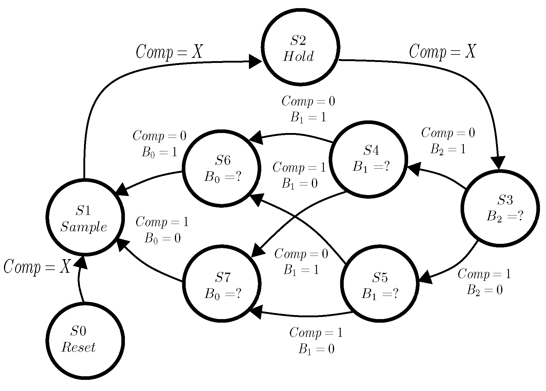
2. Successive Approximation Register (SAR) Control

Figure 3 illustrates the digital control logic of a 3-bit single-ended ADC SAR proposed in [15]. The circuit, depicted in Figure 2b, uses a shift register at the top, transferring the HIGH logic state from the first flip-flop to the last in cascade mode. The flip-flops Q outputs serially set “1” during one clock cycle, while the corresponding Q n triggers the lower circuit named the “code register”. This code register updates the corresponding flip-flop according to the resulting comparator bit and control signal for the analog switches. At the end of each conversion cycle, the value in the code register represents the digitally converted word ( B 2 , B 1 and B 0 ). Figure 2a shows the signal switch control, including switching signals for the corresponding voltage to the bottom plate capacitors (e.g., S 2 [ S 2 2 , S 2 1 , S 2 0 ] ), including the sample and hold stages. The circuit in Figure 2 is a typical choice for its simplicity and ease of understanding in SAR ADCs with 5–10 bits of resolution. Some analog designers prefer the full custom design of the digital blocks to implement the SAR logic control. Increasing the ADC resolution spec (more than 10-bit) constrains the SAR logic digital components and increases interconnections. Moreover, if the designer projects a fully differential structure with a bipolar input signal, the implementation and time for designing the logic SAR can significantly increase due to the non-linear workflow.
To render a clear description for the SAR logic in Figure 2, let us identify the B o u t and control switching S 2 n to the bottom plate in 4 C u trough expressions (1)–(4).
B o u t n ( k ) = B o u t n ( 5 ) k = 1 B o u t n ( k 1 ) k n + 2 C o m p ¯ k = n + 2
S 2 0 ( k ) = 0 k = 1 , 2 1 k = ( n 1 ) S 2 0 ( k 1 ) C o m p ¯ k = n + 2 S 2 0 ( k ) k n + 2
S 2 1 ( k ) = 1 k = 1 0 1 < k
S 2 2 ( k ) = 1 k = 1 0 k = 2 S 2 2 ( k 1 ) C o m p k = n + 2 S 2 2 ( k ) k n + 2
where k represents the discrete time of the clock signal control, n is the bit position in the SAR converter digital output B o u t ( k ) , and  C o m p is the comparator logic output. At time k = 1 , the sample stage is set, and the vector B o u t holds the previous conversion value for each bit position. For  k n , the output vector B o u t remains unchanged. This process bins the hold and conversion stage while other bits are determined. Finally, when k = n , the position n in vector B o u t takes on the comparator logic output. The expressions match the logic sequence for the SAR register in Figure 2. Therefore, it is possible to describe the switching control signal behavior through the nonlinear set of functions of the comparator state and the previous control signal. Note the design of cumbersome state machines is not a direct approximation, and the Hardware Description Language provides a good solution. Finite State Machines (FSMs) describe algorithms with multiple branches and nonlinear dependencies on previous states. For the present case, the signal S 2 0 , S 2 1 ( k ) , S 2 2 ( k ) correspond to the G N D , V i n and V r e f respectively.
Figure 3 displays a new Finite State Machine suggested in this paper for the ADC SAR circuit in Figure 2a. State machines can simplify heavy workflows involving multiple loops and branch logic when the workflow must respond to signals such as the comparator output, reset, enable, and digital redundancies or calibration schemes. These features denote an event-driven workflow. The Verilog code in Listing Section 2 represents the FSM shown in Figure 3. The description includes two blocks: asynchronous assignment and synchronous assignment. In the asynchronous assignment block, a case statement covers all seven stages of ADC conversion depicted in Figure 3, the assigned values in S 2 , S 1 , S 0 , S 00 correspond to the nonlinear equations. For instance, an if-statement determines the value of B o u t at each stage based on the comparator output value. The synchronous block includes the signals c l k and r e s e t to assign the current stage and transition to the next stage on each cloack rising edge.
Listing 1. FSM Logic SAR for ADC 3 bits single-ended Unipolar.
Electronics 13 02756 i001
The automatic tools for digital circuit design facilitate the physical implementation of weighty SAR logic and save time in the overall ADC SAR design. Within this context, a designer sets constraints in the digital implementation, such as optimizing the clock signal and determining the delay response and the times of rising and falling outputs of the SAR logic. Although the automatic digital design flow is used in many works to implement SAR logic, details about its implementation, the type and langueage of description are typically unexplored. This work presents an alternative to implementing digital SAR control, with the possibility of adding more states to calibrate the converter in future designs. The following Section will present an extension of this SAR logic for a fully differential architecture, considering biomedical specifications in the design.

3. The ADC SAR Circuit Design

The resolution and low power consumption provide SAR ADCs with biomedical application specifications for autonomous and networking. Table 2 shows the bandwidth and amplitudes of the most important bioelectrical signals. The bandwidth resides in the 0.01   Hz to 15 k Hz and amplitude ranges from 1 μV to 100 m V . This consideration locates the ADC SAR performance appropriate to the electrical characteristic of bioelectrical signals.
Figure 4 shows a bipolar fully differential SAR ADC with a 14-bit traditional ADC SAR architecture working as a balancing. The Sample and Hold (S&H) stage stores the input, initially comparing with half the reference voltage 1 2 V r e f (the reference voltage is the maximum amplitude of the input signal frame). If the input signal is larger than the first reference, the digital/analog converter (DAC) keeps the 1 2 V r e f weight on the scale. Otherwise, for the following comparison, the DAC adds a new weight of 1 4 V r e f and repeats the bitwise process. This approximation continues by storing the charge in the capacitor array in Figure 4. The ADC SAR of this work considers a resolution structure of 14 bits to ensure the target resolution. The sample rate considers an oversampling factor achieving an ENoB of 14 bit, with a signal-to-noise rate of ( S N R N = 98.02 dB ). Following the expression for oversampled signal-to-noise ratio ( S N R O S ) Equation (5),
SNR OS = 98.02 dB = 6.02 · ENoB + 1.25 + 10 log 10 ( OSR ) .
From this expression the oversampling factor is OSR = 16 , where ENoB = 14 bit . According to Table 2, this work considers a fundamental frequency f o = 13.760 kHz for biomedical signals, with 80 kHz of Bandwidth (BW) and sampling frequency f s = 2.56 MHz .
A fully differential circuit offers benefits by canceling the common mode noise, including the fully differential comparator. The differential SAR uses two matrices of split capacitances per input terminal with the corresponding differential logic Successive Approximation Register (SAR). For this implementation the voltage references are: V r e f + = + 1.8 V, V r e f = 0 V, V c m = 0.9 V suggested for a CMOS UMC 180 n m . The following subsections detail the design considerations in this ADC SAR implementation.

3.1. DAC Split Capacitor Array

The main advantage of using charge sharing in ADCs is low power consumption. However, as the number of bits increases, the capacitive load and DAC capacitor area exponentially increase. A solution for the DAC area is the charge scaling DAC with the split array configuration. Figure 4 shows the two matrix structures (MSBs and LSBs) with capacitive coupling. The recent SAR ADC improvements focus on the DAC structure because this block performs the sampling and hold (S&H), sum, and digital to analog conversion in a single step. An initial consideration for the design is the unitary capacitance C U for the DAC Split Array block. The ideal scenario is the minimum capacitance for a MIMCAP on UMC180nm (100 f F ).
However, according to [16], the approximation of the minimum C u capacitance ( C m i n ) must consider the temperature, mismatch effects, the typical capacitive density of the technology, resolution, error budget to the thermal noise, and voltage reference values. The C m i n considers all of these with:
C min = max C m m in , C n m in
where C m m in is the matching-determined minimum unit capacitance, and C n m in is the unitary capacitance by the capacitors array’s thermal noise. Table 3 resumes the minimum unitary capacitance parameters. For a DAC 14 bit resolution, the thermal and voltage reference is 16 f F , and the process minimum capacitance successfully achieves the limit with a minimum of 18 f F . As a rule of thumb to ensure a 1 2 L S B error budget: C u = 4 C min = 72   f F . However, according to the design rules in the UMC180nm [16] process, the minimum allowed capacitance is 100 f F . The switches associated with the DAC capacitors are complementary, and the input front-end sampling switches use the bootstrap scheme. The bootstrapped switch design utilizes the configuration and compensation scheme published in [17] to reduce nonlinearities. Additionally, the transmission gate switches, connecting the DAC assembly to different voltage references ( V r e f ± , V c m ), consider a good ohmic contact maintaining the source and bulk terminal at the same potential to minimize body-effect nonlinearities. Reference voltages remain constant when compared with the variation of the input voltage range, allowing simulations with PVT variations to evaluate changes in the transmission gate resistance R o n p , n . The transmission gate circuit design considers a safe range to reduce the nonlinearities caused by V g s , mitigating harmonic distortion.

3.2. Nonlinear Successive Approximation Logic

The logic SAR subsystem, as shown in Figure 5, has three input ports: R e s e t , C l k , and the two-bit C o m i n sequence produced by the fully differential comparator. The state machine has seven outputs contolling the fully differential DAC array. The output C RDY indicates the availability of the ADC conversion, and the output signal S enables the DAC capacitor top plates to connect to the common-mode voltage V c m at the sampling state. The bus C V i n controls the bootstrapping switches, and the buses C V r 1 and C V r 2 control differential voltage references to the capacitor bottom plate switches. Figure 5 also shows the logic SAR sequence where the clock signal rising edge changes the states. The reset input commands the system to the initial stage. The following process is to Sample where the C V i n FSM output enables all the bootstrapped switches, connecting the bottom plates to V i n + , V i n according to the schematic in Figure 4. In this first cycle, the S output switches the DAC LSBs section to the common-mode V c m through the center-located switches. The second cycle takes the FSM to the H o l d state with a do not care for the values of C o m i n . In this state, the FSM executes three processes: (i) holds the sampled input, (ii) detects the sign of the input signal ( V i n + > V c m or V i n > V c m ), and (iii) sets the MSB value ( B [ 13 ] ).
The sign value results from the hold process by disabling the bootstrapped switches with C V i n , and the S output disconnects the LSB capacitor top plates. In this process, C V c m connects all the bottom plate capacitors to V c m , and the top plates are in floating condition, holding the sampled input voltage at nodes V y p and V y n . The bottom plate connection to the common-mode voltage subtracts 1 2 V r e f to the sampled input value. With this process, the node V y p , n exhibits a differential of potential equal to V i n ± 1 2 V r e f V c m , the comparator determines the input voltage sign and the path where the conversion starts by establishing B [ 13 ] in ‘1’ or ‘0’, as well as voltage reference V r e f ± (e.g., shaded states in Figure 5). According to the previous state, the next state will be S 3 n or S 3 p . The control signal C V c m [ 13 ] = 0 turns off the 64 C u capacitor in the MSBs DAC array section while other capacitors remain connected to V c m . Simultaneously, C V r 1 , 2 [ 13 ] = 1 enables the switches connecting the 64 C u bottom plate to V r e f ± . The voltage V i n ± 1 4 V r e f V c m appears at node V y p , n to calculate the B [ 12 ] bit.
When C o m i n = 10 the output B [ n ] is ‘1’ and for C o m i n = 01 the output B [ n ] is ‘0’. There are two points to notice in the successive approximation: (i) in the left side of the FSM diagram in Figure 5, the control bus C V c m [ 13 : 0 ] disconnects the capacitors from V c m and connect to reference voltage according to Figure 4, i.e., when the bit B [ n ] is ‘1’, the next state returns the C V c m [ n ] to 1 while returning if C V r 2 = 0 . Both signals maintain the previous state if B [ n ] = 0 . And ii) On the other hand, on the right side of the FSM for B [ n ] = 1 , the control signal states are at C V c m [ n ] = 0 and C V r 2 [ n ] = 1 and for B [ n ] = 0 signals will be the opposite value. This configuration fulfills the expressions (7) and (8) for V i n + > V c m , and (9) and (10) for V i n > V c m , where V y p and V y n represent the comparator inputs.
V y p ( k ) = V i n + k = 1 V y p ( 1 ) 1 2 V D D k = 2 V y p ( k 1 ) + 1 2 ( k 1 ) V D D 2 < k
V y n ( k ) = V i n k = 1 V y n ( 1 ) + 1 2 V D D k = 2 V y n ( k 1 ) 1 2 ( k 1 ) V D D 2 < k
V y p ( k ) = V i n + k = 1 V y p ( 1 ) + 1 2 V D D k = 2 V y p ( k 1 ) 1 2 ( k 1 ) V D D 2 < k
V y n ( k ) = V i n k = 1 V y n ( 1 ) 1 2 V D D k = 2 V y n ( k 1 ) + 1 2 ( k 1 ) V D D 2 < k
The states following S 3 p , n in Figure 5 depend on two possible decisions for each stage. For instance, Figure 6 presents a transient simulation where B [ 13 ] = 0 and B [ 12 ] = 1 and the next state will be S 4 n 1 . The values for the C V c m [ 13 ] and C V r 2 [ 13 ] return to ‘1’ or ‘0’ respectively (left side of FSM), while setting C V c m [ 12 ] = 0 and C V r 2 [ 12 ] = 1 to generate V i n + 1 4 V r e f 1 8 V r e f V c m at node V y p and V i n + 1 4 V r e f + 1 8 V r e f + V c m at node V y n and calculate the B [ 11 ] bit. The process is iterative up to the S 15 x 1 state calculating the LSB. Finally, the S 16 x state in Figure 5 discharges the capacitor C u for a new conversion. The FSM considers the DAC’s fully differential feature with the Verilog description and the Cadence Genus digital synthesis with the UMC180nm CMOS technology. The Data Converter in this work uses the digital synthesis system requiring 423 standard cells, 74 sequential cells, 293 logic, and 56 inverters. The digital system section consumes 27.015 nW at 30.7   M Hz of static power. The voltage comparator design must be robust for good performance with the proposed state machine.
Notwithstanding the digital logic SAR in full-custom design can achieve a high transistor density, it is a long, error-prone process with a high development risk, especially when the ADC architecture resolution is beyond 12 bits and with fully differential architectures; the number of control lines increases considerably. An ADC SAR of 14-bit resolution requires at least eight control signals per capacitor (considering the complementary signals); there are 14 capacitors, and the control lines duplicate for a fully differential architecture. Also, it is essential to consider the extra circuit to avoid the overlap phases on control signals. The finite state machine proposed in this work uses the technology’s CAD place and route of standard cells, and the time-to-develop design is reduced significantly. Table 4 shows the time to complete the digital place and route design flow in this work. According to the [18] report, using the fully customized method for designing digital circuits takes, on average, twice as long as using standard cells. The design in this work takes approximately 2 h to interconnect the digital logic SAR with the analog part. The FSM proposed in this work speeds up the digital logic SAR and layout design.

3.3. Fully Differential Robust Comparator Design

The SAR ADCs comparator’s specifications, such as gain, slew rate, and time response, limit the converter’s resolution. However, these are possible with a preamplifier followed by a Latch. The first step in designing the voltage comparator is the SAR ADC sampling time F s . For a 14 bit of resolution with 16 clock cycles per conversion and for F s =   1.92   M Hz and f comp =   30.7   M Hz . The comparator and latch stages must cover this limit frequency and consider the LSB quantization level of 109 μV.
The proposed comparator in Figure 7 uses a complementary structure of n-type and p-type differential pairs. It adopts the continuous-time and positive feedback high-gain comparator in [19]. The basic circuit function is a latch amplifier with hysteresis. The latch-amplifier phase depends on the α factor in the differential gain as A d = ( g m 1 / g m 3 ) ( 1 α ) 1 , where α = ( W / L ) 5 / ( W / L ) 3 . With α 1 , the comparator latches the output voltages as A d . The symmetrical feature renders the proposed comparator robust to Process Voltage and Temperature disturbances. The complementary differential pairs mirror the outputs with m 15 , m 16 , m 17 and m 18 and the differential gain is:
A d = g m 1 · g m 15 g m 3 · g d s 15 1 1 α
The topology maintains a close relationship between the m 5 and m 3 transistor’s sizes, increasing the differential gain with the current mirror at the output stage. The equal dimensions ensure symmetry and robustness for the amplifier and latch operation.
The comparator design in CMOS UMC180nm with post-layout results exhibit a 20 ns @109μVpp step response, with a Δ D e l a y = 5 ns . The variations in the output dynamic range are Δ O D R = 358     μ V and the voltage offset is 24.7   μ V with a standard deviation below 5   μ V .
The proposed comparator consumes 143   μ W of static power and improves the robustness and ODR for the state-of-the-art comparators [19]. It is possible to enhance the comparator’s sensitivity with additional pre-amplifiers. Figure 8 shows the static response under process and temperature variations. The corners for this result are Slow-Slow, Slow-Fast, Typical-Typical, and Fast-Slow, and the temperature cases −40 °C, 60 °C and, 120 °C. Figure 8a depicts critical differences compared with the proposed complementary architecture shown in Figure 8b. Figure 8c illustrates a Monte Carlo analysis, where the mismatch transistor effect increases variations in latch offset within only a range of ± 6 mV in the presented scheme. With a preamplifier stage the comparator reaches a sensitivity of 80   μ V with a delay of 1 ns and Δ D e l a y = 5 ns , the Δ O D R = 65 ns and the voltage offset is 10   μ V , with Δ V O S = 15   μ V . The pre-amplifier stage uses the proposed topology with α = 0.7 , maintaining the robust performance with 97   μ W of power consumption. The proposed continuous comparator and FSM are designed to prevent metastable outputs ( C o m p = 00 ”, C o m p = 11 ”). If this occurs, the finite state machine does not progress to the next state, preventing conversion errors.

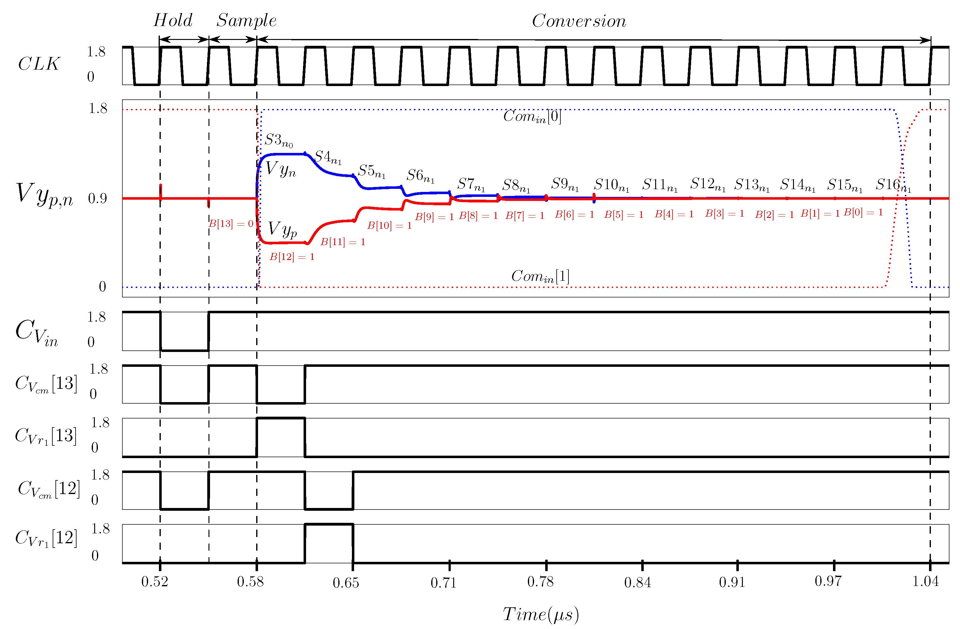
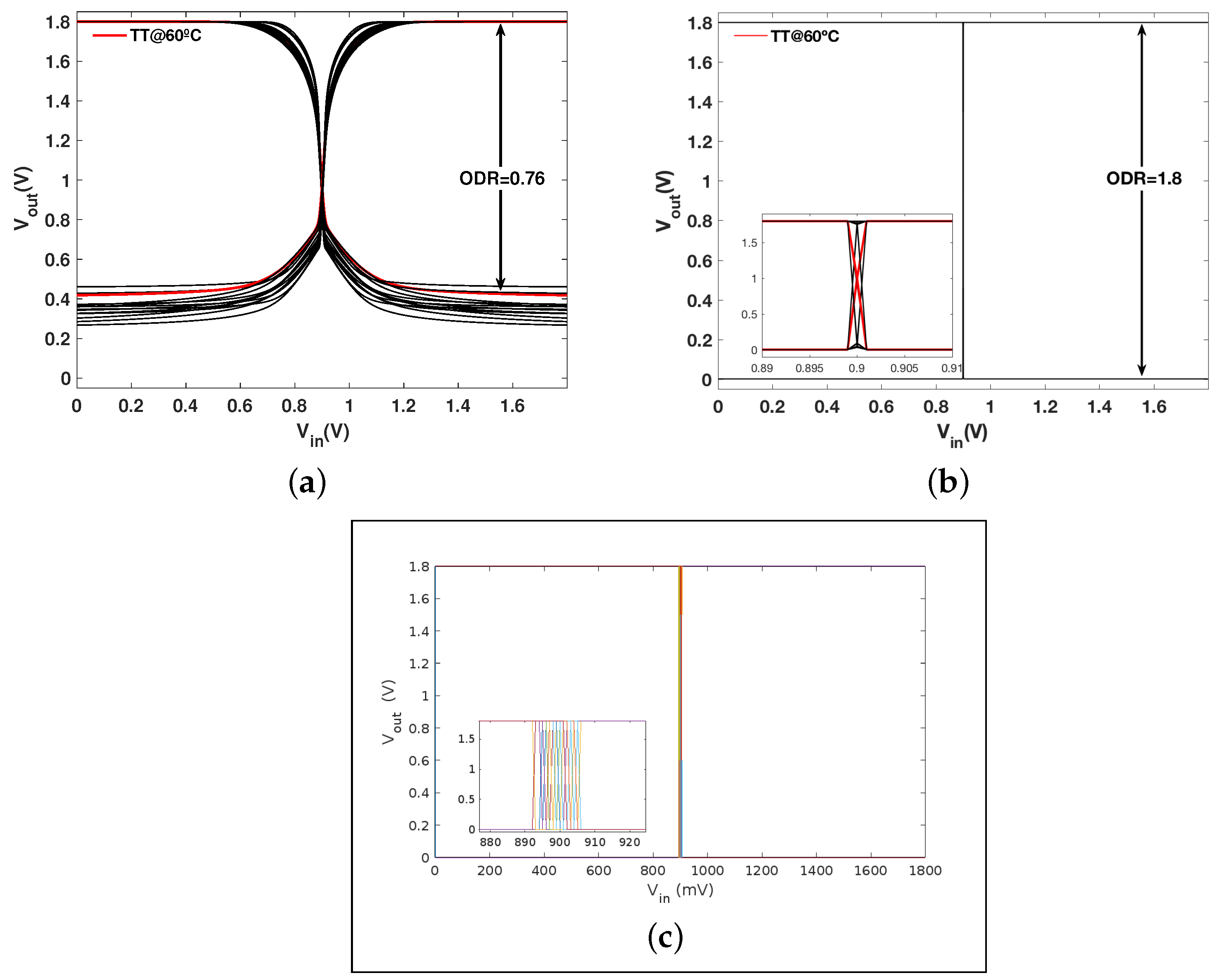
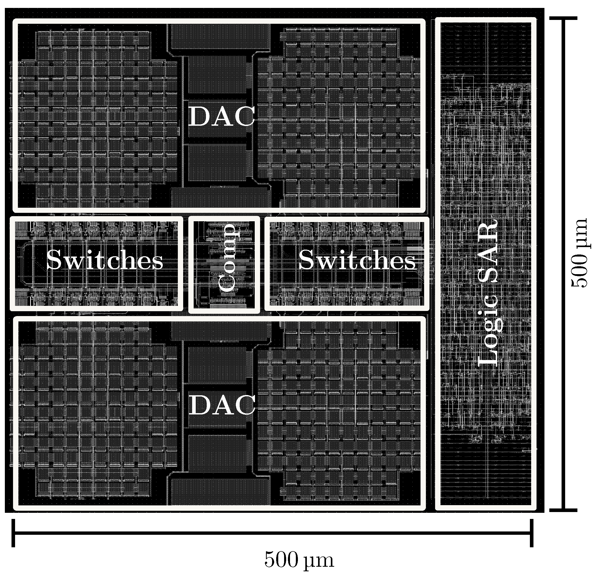
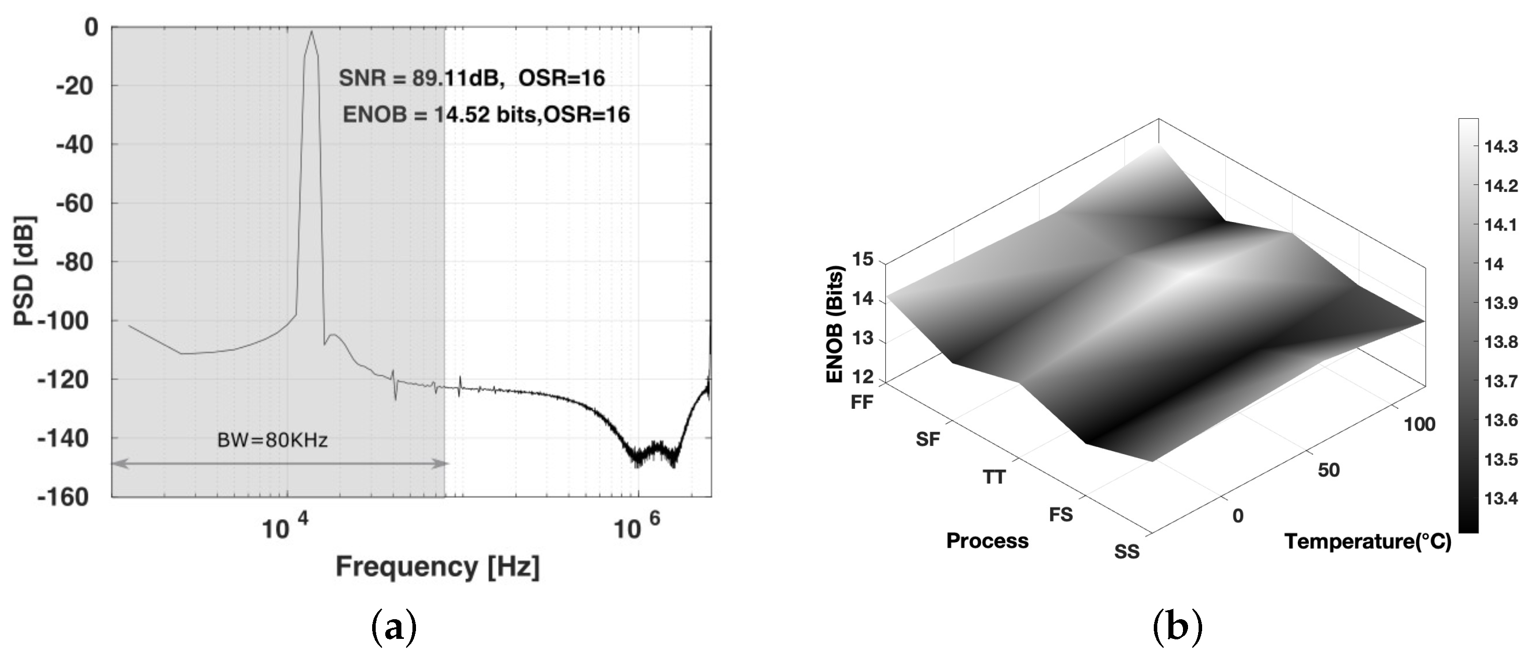
4. Post-Layout Characterization and Results

The proposed 14 bit SAR ADC design uses the Finite State Machine as a novel logic SAR, the robust comparator, and switches configuration of this work in a UMC180nm CMOS technology. The layout fits in 0.25 mm2 (500 μm × 500 μm). The layout in Figure 9 considers a symmetrical disposition with a common centroid for the capacitive DAC array. The SAR ADC layout incorporates dummy structures for the capacitive network, with the comparator at the center alongside dummy transistors.
The post-layout simulation for a 80 k Hz bandwidth and Oversampling Rate (OSR = 16) exhibits the spectrum in Figure 10a. The sampling frequency for this test is 2.56MS/s with a 13.760 kHz sinusoidal input signal, which is below the bandwidth limit to observe possible harmonic content. The post layout result yields 14.52 bit of ENoB considering the Typical-Typical statistical models from the UMC180nm process design kit at 60 °C.
A Process and Temperature variation test validates the effectiveness of the proposed control logic SAR and the robustness of the comparator. Figure 10b shows the corner resolution with a distribution between 13.31 bit to 14.52 bit for 24 post-layout simulation corner tests (in transient analysis). The critical corner in this statistical test is the SF process at −40 °C. The SF and FS corners for any temperature show ENoBs below 13.5 Bits, while TT, SS, and FF at 60 °C and 120 °C improve the ENoB because the response of the continuous comparator presents a minimum offset in these corners, changing the sensitivity of the comparator for the less significant bits.

Comments on the Simulation Results

Table 5 summarizes the performance of the ADC converter using the proposed SAR logic. The Walden ( FoM W ) and Schreier ( FoM S ) [5] Figures of Merit (FoM) exhibit good performance of this work. The proposed data converter achieves a balance between sampling rates and power consumption. Furthermore, the proposed design presents robustness with process and temperature variations, typically unexplored in most publications. Despite achieving a high resolution (ENOB > 14b), it is widely recognized that during the manufacturing process, about 4 or 5 bits are lost when there is no calibration scheme [20,21,22,23]. However, the suggested finite state machine (FSM) can be adjusted to work with a calibration scheme. For instance, in [20], the calibration method uses the occurrence of metastability in the comparator and the intrinsic noise to calibrate the DAC array without changing its structure. In this case, only additional states need to be included for calibration during each conversion.

5. Conclusions

This work presents the design of a traditional 14 bit ADC SAR with a novel continuous comparator robust to PT variations and a novel Successive Approximation control logic based on a non-linear logic SAR. This research highlights the problems arising from a high-resolution and fully differential version of the SAR logic construction. The proposed digital logic considers forbidden states by observing the actual and previous conversion values. Post-layout simulations exhibit a 14.52 bit of ENoB and robustness to process and temperature variations, with a 0.63 bits mean loss; however, with mismatch effects, is probably to lose 3 to 5 bits. The ADC uses 0.25 mm2 in area and consumes 310.3   μ W at a 2.56   M Hz sampling frequency. The achieved SNDR is 84.66 dB, resulting in Schreier FoM is 165.76 dB, and Walden FoM of 7.04 fJ conv−lev. The proposed Finite State Machine is an excellent choice for implementing SAR logic control in any ADC converter.

Author Contributions

Conceptualization, G.D.L.F.-C. and V.R.G.-D.; Methodology, G.D.L.F.-C., G.E.F.-V., A.D.-M. and V.R.G.-D.; Software, V.R.G.-D.; Validation, G.D.L.F.-C. and V.R.G.-D.; Formal analysis, G.D.L.F.-C. and V.R.G.-D.; Investigation, G.D.L.F.-C. and V.R.G.-D.; Resources, G.E.F.-V., A.D.-M. and V.R.G.-D.; Data curation, G.D.L.F.-C.; Writing—original draft, G.D.L.F.-C. and V.R.G.-D.; Writing—review & editing, G.E.F.-V. and V.R.G.-D.; Visualization, A.D.-M.; Supervision, G.E.F.-V.; Project administration, A.D.-M. All authors have read and agreed to the published version of the manuscript.

Funding

The authors of this work thank the financial support to BUAP, VIEP-BUAP and CONAHCyT Mexico through Science of Frontiers Project PCC-2022-319601 and the Postdoctoral grant 3969891.

Data Availability Statement

Data from this research is available upon reasonable request.

Conflicts of Interest

The authors declare no conflicts of interest.

References

  1. Lakshmi, P.V.; Musala, S.; Srinivasulu, A.; Ravariu, C. Design of a 0.4 V, 8.43 ENOB, 5.29 nW, 2 kS/s SAR ADC for Implantable Devices. Electronics 2023, 12, 4691. [Google Scholar] [CrossRef]
  2. Chung, Y.H.; Chiang, M.S. A 12-Bit Synchronous-SAR ADC for IoT Applications. In Proceedings of the 2019 IEEE International Symposium on Circuits and Systems (ISCAS), Hokkaido, Japan, 26–29 May 2019; pp. 1–5. [Google Scholar] [CrossRef]
  3. Wei, Y.; Wu, T.; Ma, S.; Ren, J. A Multi-channel 12-bits 100MS/s SAR ADC in 65nm CMOS. In Proceedings of the 2023 IEEE 15th International Conference on ASIC (ASICON), Nanjing, China, 24–27 October 2023; pp. 1–4. [Google Scholar] [CrossRef]
  4. Meier, D.; Ackermann, J.; Olsen, A.; Kristian, H.; Berge, H.; Hasanbegovic, A.; Altan, A.; Azman, S.; Najafiuchevler, B.; Talebi, J.; et al. SIPHRA 16-Channel Silicon Photomultiplier Readout ASIC. In Proceedings of the AMICSA and DSP 2016, Gothenburg, Sweden, 12–16 June 2016. [Google Scholar] [CrossRef]
  5. Murmann, B. ADC Performance Survey 1997–2023. Available online: https://github.com/bmurmann/ADC-survey (accessed on 1 February 2024.).
  6. Mendonca, L.; Bhandarkar, R. Implementation of SAR ADC for Biomedical Applications—A Review. In Advances in Communication, Signal Processing, VLSI, and Embedded Systems; Kalya, S., Kulkarni, M., Shivaprakasha, K., Eds.; Springer: Singapore City, Singapore, 2020; pp. 151–159. [Google Scholar]
  7. Hu, J.; Li, D.; Liu, M.; Zhu, Z. A 10-kS/s 625-Hz-Bandwidth 65-dB SNDR Second-Order Noise-Shaping SAR ADC for Biomedical Sensor Applications. IEEE Sensors J. 2020, 20, 13881–13891. [Google Scholar] [CrossRef]
  8. Sadollahi, M.; Hamashita, K.; Sobue, K.; Temes, G.C. An 11-Bit 250-nW 10-kS/s SAR ADC With Doubled Input Range for Biomedical Applications. IEEE Trans. Circuits Syst. I Regul. Pap. 2018, 65, 61–73. [Google Scholar] [CrossRef]
  9. Hu, Y.; Chen, L.; Chen, H.; Wen, Y.; Zhang, H.; Wu, Z.; Li, B. A 7.6-nW 1-kS/s 10-bit SAR ADC for Biomedical Applications. In Proceedings of the 2019 IEEE Asia Pacific Conference on Circuits and Systems (APCCAS), Bangkok, Thailand, 11–14 November 2019; pp. 129–132. [Google Scholar] [CrossRef]
  10. Wang, S.H.; Hung, C.C. A 0.3V 10b 3MS/s SAR ADC With Comparator Calibration and Kickback Noise Reduction for Biomedical Applications. IEEE Trans. Biomed. Circuits Syst. 2020, 14, 558–569. [Google Scholar] [CrossRef] [PubMed]
  11. De La Fuente-Cortes, G.; Espinosa Flores-Verdad, G.; Gonzalez-Diaz, V.R.; Diaz-Mendez, A. A new CMOS comparator robust to process and temperature variations for SAR ADC converters. Analog Integr. Circuits Signal Process. 2017, 90, 301–308. [Google Scholar] [CrossRef]
  12. Jie, L.; Tang, X.; Liu, J.; Shen, L.; Li, S.; Sun, N.; Flynn, M.P. An Overview of Noise-Shaping SAR ADC: From Fundamentals to the Frontier. IEEE Open J. Solid-State Circuits Soc. 2021, 1, 149–161. [Google Scholar] [CrossRef]
  13. Kim, S.B.; Kwon, K.W. A hybrid ADC combining capacitive DAC-based multi-bit/cycle SAR ADC with flash ADC. In Proceedings of the 2016 International Conference on Electronics, Information, and Communications (ICEIC), Harbin, China, 20–22 August 2016; pp. 1–4. [Google Scholar] [CrossRef]
  14. Kobayashi, Y.; Matsuura, T.; Kishida, R.; Hyogo, A. Investigation of Hybrid ADC Combined with First-order Feedforward Incremental and SAR ADCs. In Proceedings of the 2019 International Symposium on Intelligent Signal Processing and Communication Systems (ISPACS), Taipei, Taiwan, 3–6 December 2019; pp. 1–2. [Google Scholar] [CrossRef]
  15. Anderson, T.O. Optimum Control Logic for Successive Approximation Analog-to-Digital Converters. Deep Space Netw. Prog. Rep. 1972, 13, 168–176. [Google Scholar]
  16. Yue, X. Determining the reliable minimum unit capacitance for the DAC capacitor array of SAR ADCs. Microelectron. J. 2013, 44, 473–478. [Google Scholar] [CrossRef]
  17. Qin, C.; Cai, Z. Bootstrapped Complementary Switches for High-Precision Sampling. In Proceedings of the 2023 IEEE International Symposium on Circuits and Systems (ISCAS), Jeju, Korea, 24–25 October 2023; pp. 1–5. [Google Scholar] [CrossRef]
  18. Eriksson, H.; Larsson-Edefors, P.; Henriksson, T.; Svensson, C. Full-custom vs. standard-cell design flow - an adder case study. In Proceedings of the ASP-DAC Asia and South Pacific Design Automation Conference, New York, NY, USA, 21–24 January 2003; pp. 507–510. [Google Scholar] [CrossRef]
  19. Gregorian, R. Introduction to CMOS OPAMPs and Comparators; John Wiley & Sons: Hoboken, NJ, USA, 1999. [Google Scholar]
  20. Chen, L.; Ma, J.; Sun, N. Capacitor mismatch calibration for SAR ADCs based on comparator metastability detection. In Proceedings of the 2014 IEEE International Symposium on Circuits and Systems (ISCAS), Melbourne, Australia, 1–5 June 2014; pp. 2357–2360. [Google Scholar] [CrossRef]
  21. Fateh, S.; Schönle, P.; Bettini, L.; Rovere, G.; Benini, L.; Huang, Q. A Reconfigurable 5-to-14 bit SAR ADC for Battery-Powered Medical Instrumentation. IEEE Trans. Circuits Syst. I Regul. Pap. 2015, 62, 2685–2694. [Google Scholar] [CrossRef]
  22. Yang, X.; Zhao, M.; Dong, Y.; Wu, X. A 14.9 μW analog front-end with capacitively-coupled instrumentation amplifier and 14-bit SAR ADC for epilepsy diagnosis system. In Proceedings of the 2016 IEEE Biomedical Circuits and Systems Conference (BioCAS), Shanghai, China, 17–19 October 2016; pp. 268–271. [Google Scholar] [CrossRef]
  23. Shen, Y.; Li, H.; Bindra, H.S.; Cantatore, E.; Harpe, P. A 14-Bit Oversampled SAR ADC With Mismatch Error Shaping and Analog Range Compensation. IEEE Trans. Circuits Syst. II Express Briefs 2023, 70, 1719–1723. [Google Scholar] [CrossRef]
Figure 1. ADC SAR in biomedical signal conditioning circuit.
Electronics 13 02756 g001
Figure 2. Successive approximation analog-to-digital converter 3 bits (a) conceptual circuit -charge redistribution technique (b) Logic Control SAR for 3 bits ADC [15] .
Electronics 13 02756 g002
Figure 3. Logic Control SAR Finite State Machine for 3 bits ADC.
Electronics 13 02756 g003
Figure 4. Successive Approximation ADC Block-Level representation with Split array capacitor.
Electronics 13 02756 g004
Figure 5. Finite State Machine for the Successive Approximation Logic. The colored shapes highlight the sequence evolution. The first state considers a differential input where V i n > V c m , and the second a differential input where V i n + > V c m .
Electronics 13 02756 g005
Figure 6. Transient ADC SAR Converter response, V i n + = V c m L B S , V i n = V c m L B S . The colored lines highlight the fully differential conversion steps.
Electronics 13 02756 g006
Figure 7. Scheme of the proposed continuous-time comparator.
Electronics 13 02756 g007
Figure 8. Comparator DC sweep response comparison. (a) PT variations performed to the comparator in [19]. (b) PT variations with the proposed comparator, including zoomed view. (c) Monte Carlo analysis of the proposed comparator, including zoomed view.
Electronics 13 02756 g008
Figure 9. Layout design, including the DAC and proposed Successive Approximation Logic.
Electronics 13 02756 g009
Figure 10. FFT results at 2.56 MS/s, F i n = 13.760 kHz. (a) ENoB at TT, 60 °C. (b) Effective number of bits, PT variations.
Electronics 13 02756 g010
Table 1. ADC SAR features in the Biomedical Applications state-of-the-art.
Specification[7][8][9][10]
ArchitectureNSSingleSingleSingle
SAREndedEndedEnded
Technology (nm)18018018090
Resolution (Bits)7111010
Bandwidth (MHz)0.000625
Supply Voltage (V)1.00.751.80.3
Sampling Rate (MS/s)0.010.010.0013
Core area (mm2)0.120.1280.150.08
ENoB (Bits)10.59.767.29.08
Power consumption (μW)0.090.250.766.6
FoM (fJ/conv-lev)5028.851.74.065
Table 2. Summary of electrical and biomedical signals features.
SignalBandwidth
(Hz)
Amplitude
Range
Electroencephalogram (EEG)0.01 to 150<1 μV to 1 mV
Electrooculography (EOG)0.01 to 50<10 μV to 10 mV
Electrocardiography (ECG)0.01 to 300<50 μV to 10 mV
Electromyography (EMG)-Internal0.01 to 15 k<200 μV to 20 mV
Electromyography (EMG)-External10 to 8 k<10 μV to 100 mV
Table 3. Considerations for the minimum unitary capacitance in UMC180nm.
ParameterExpressionValue
Bits resolutionN14
Voltage reference V r e f 1.8 V
Capacitance density C D 100 fF
C m m i n C D 3.5 2 N + 2 ( 2 N 1 + ( 2 1 ) 2 N ( 2 1 ) 2 N 2 18 fF
C n m i n 4 K T 2 N + 4 V r e f 2 16 fF
Table 4. Setup time in digital design flow Logic SAR.
DesignFlow StepTime
LogicDesign Entry (HDL)2 h
Logic Synthesis2 min
Post-synthesis simulation40 min
PhysicalFloor Planning10 min
Placement and routing2 min
Post-Layout simulation40 min
Interconnections1 h
Table 5. Propouse ADC SAR for Biomedical Applications.
SpecificationThis Work
ArchitectureFully Differential
Technology (nm)180
Supply Voltage (V)1.8
Resolution (Bits)14
Sampling Rate (MS/s)2.56
Core area (mm20.25
SNDR (dB)84.66
Power consumption (μW)310.3
OSR16
Bandwidth (MHz)0.08
ENoB (Bits)14.07
F O M w ( f J / conv - lev ) 165.76
F O M s (dB) 165.76
F O M w = P o w e r F s 2 E N o B . F O M s = S N D R + 10 l o g ( B W / 2 P o w e r ) .
Disclaimer/Publisher’s Note: The statements, opinions and data contained in all publications are solely those of the individual author(s) and contributor(s) and not of MDPI and/or the editor(s). MDPI and/or the editor(s) disclaim responsibility for any injury to people or property resulting from any ideas, methods, instructions or products referred to in the content.

