Article

Schottky Barrier Formation Mechanism and Thermal Stability in Au-Free Cu/Metal–Silicide Contacts to GaN-Cap/AlGaN/AlN-Spacer/GaN-on-Si Heterostructure

1
Łukasiewicz Research Network—Institute of Microelectronics and Photonics, Al. Lotników 32/46, 02-668 Warsaw, Poland
2
Institute of Microelectronics and Optoelectronics, Warsaw University of Technology, Koszykowa 75, 00-662 Warsaw, Poland
*
Author to whom correspondence should be addressed.
Electronics 2024, 13(17), 3429; https://doi.org/10.3390/electronics13173429
Submission received: 25 June 2024 / Revised: 23 August 2024 / Accepted: 26 August 2024 / Published: 29 August 2024
(This article belongs to the Special Issue New Advances in Semiconductor Devices/Circuits)

Abstract

:
In this study, metal–silicide-based contacts to GaN-cap/AlGaN/AlN-spacer/GaN-on-Si heterostructure were investigated. Planar Schottky diodes with Cu-covered anodes comprising silicide layers of various metal–silicon (M–Si) compositions were fabricated and characterized in terms of their electrical parameters and thermal stability. The investigated contacts included Ti–Si, Ta–Si, Co–Si, Ni–Si, Pd–Si, Ir–Si, and Pt–Si layers. Reference diodes with pure Cu or Au/Ni anodes were also examined. To test the thermal stability, selected devices were subjected to subsequent annealing steps in vacuum at incremental temperatures up to 900 °C. The Cu/M–Si anodes showed significantly better thermal stability than the single-layer Cu contact, and in most cases exceeded the stability of the reference Au/Ni contact. The work functions of the sputtered thin layers were determined to support the discussion of the formation mechanism of the Schottky barrier. It was concluded that the barrier heights were dependent on the M–Si composition, although they were not dependent on the work function of the layers. An extended, unified Schottky barrier formation model served as the basis for explaining the complex electrical behavior of the devices under investigation.

1. Introduction

Enhancing the efficiency of high-power electronic devices aligns with the concept of sustainable development. Next-generation devices that utilize wide-bandgap semiconductors, such as gallium nitride (GaN) or silicon carbide (SiC), can operate at higher frequencies, voltages, and temperatures [1]. Their wide adoption will reduce electric power conversion losses and mitigate the negative impact on the environment.
The progress of high-power electronics is nowadays largely influenced by the development of new electronic devices that utilize GaN epitaxial layers grown on Si substrates [2]. The important advantage of GaN-on-Si heterostructures is their relatively low cost which stems from the ability to grow GaN epitaxial layers on inexpensive, large-area Si wafers. Additional economic benefits can be realized by fabricating devices in established silicon foundries. It implies that the design of the devices must align with the standards of the Si industry. The requirement eliminates the possibility of using gold (Au) [3,4,5,6,7,8], which has proven its applicability in GaN technology, but is a serious contaminant in Si devices.
The exceptional properties of GaN are often utilized in AlGaN/GaN High Electron Mobility Transistors (HEMTs), where gold is commonly used for metallization. The solution to Au-free metallization scheme may be to replace gold with copper (Cu), which has a lower resistivity than Au, a higher thermal conductivity, and a lower cost. Several promising reports on pure Cu/(AlGaN/GaN heterostructure) Schottky contacts have been published [9,10,11]. However, thermal stability investigations demonstrated poor reliability of Cu-based Schottky junctions [12,13,14]. Cu can easily diffuse into GaN, and chemical reactions at the Cu/heterostructure interface occur at elevated temperatures [14]. Therefore, to use Cu in Schottky gate HEMTs, a specific Schottky contact is required that can block the diffusion of Cu atoms toward the substrate.
Various Au-free Schottky contacts to AlGaN/GaN heterostructures have been investigated so far. A TiN layer frequently appears in scientific reports [6,15,16,17,18,19,20,21,22,23,24], where it is used as the first layer (i.e., in contact with the heterostructure) of the stack constituting the gate or anode. There are also research reports that use Ni as the first layer, similar to typical Au/Ni/heterostructure contacts, but with various metals replacing the Au as the second (top) layer in the stack (for example, Al [25] or W [26]). Various other materials have also been tested, including Al/W [27], WC [8], and WNx [28].
However, in regard to copper metallization and thermal stability, the particularly promising materials for creating Schottky contacts are metal silicides [7,14,29]. These compounds can form contacts that are generally more thermally stable than those with pure metal layers [30]. Pure metals are also not ideal candidates for diffusion blocking layers because they can form alloys with Cu and thus serve as a medium for Cu diffusion. Our recent studies revealed that the insertion of a Pd2Si layer between the Cu overlayer and AlGaN/GaN heterostructure significantly improves the thermal stability of the Schottky electrode [14]. Furthermore, the Cu/Pd2Si Schottky electrodes revealed higher resilience to elevated temperatures compared with other Au-free contacts like TiN [24] or WC [8].
Some silicides have relatively high work functions, close to 5.0 eV [31], which are promising in terms of the expected Schottky barrier height. In our recent studies, the Cu/Pd2Si and Au/Ni contacts, exhibited similar barrier heights [14]. Yoon et al. [7] reported Cu/TiSi2 contacts with a higher barrier than the reference Au/Ni contact (despite a theoretically lower work function 4.53 eV vs. 5.01 eV). Since the Cu/metal–silicide/(HEMT heterostructure) system has not been thoroughly investigated to date, it is necessary to investigate Schottky barrier formation mechanism and the stability of such structures.
In this study, we investigated and compared Schottky planar diodes with anodes containing Cu-covered silicide layers of various metal–silicon compositions. The results enabled the classification of the metal–silicide-based contacts in terms of Schottky barrier height and leakage currents. Subsequently, the thermal stability of the selected devices was investigated by annealing in vacuum. Additionally, the work functions of the sputtered silicide layers were determined using Internal Photoemission Spectroscopy (IPS). This enhanced the discussion on the formation mechanism of the Schottky barrier. Finally, an extended model is employed to explain the dependence of the observed barrier height on the parameters of the technological process.

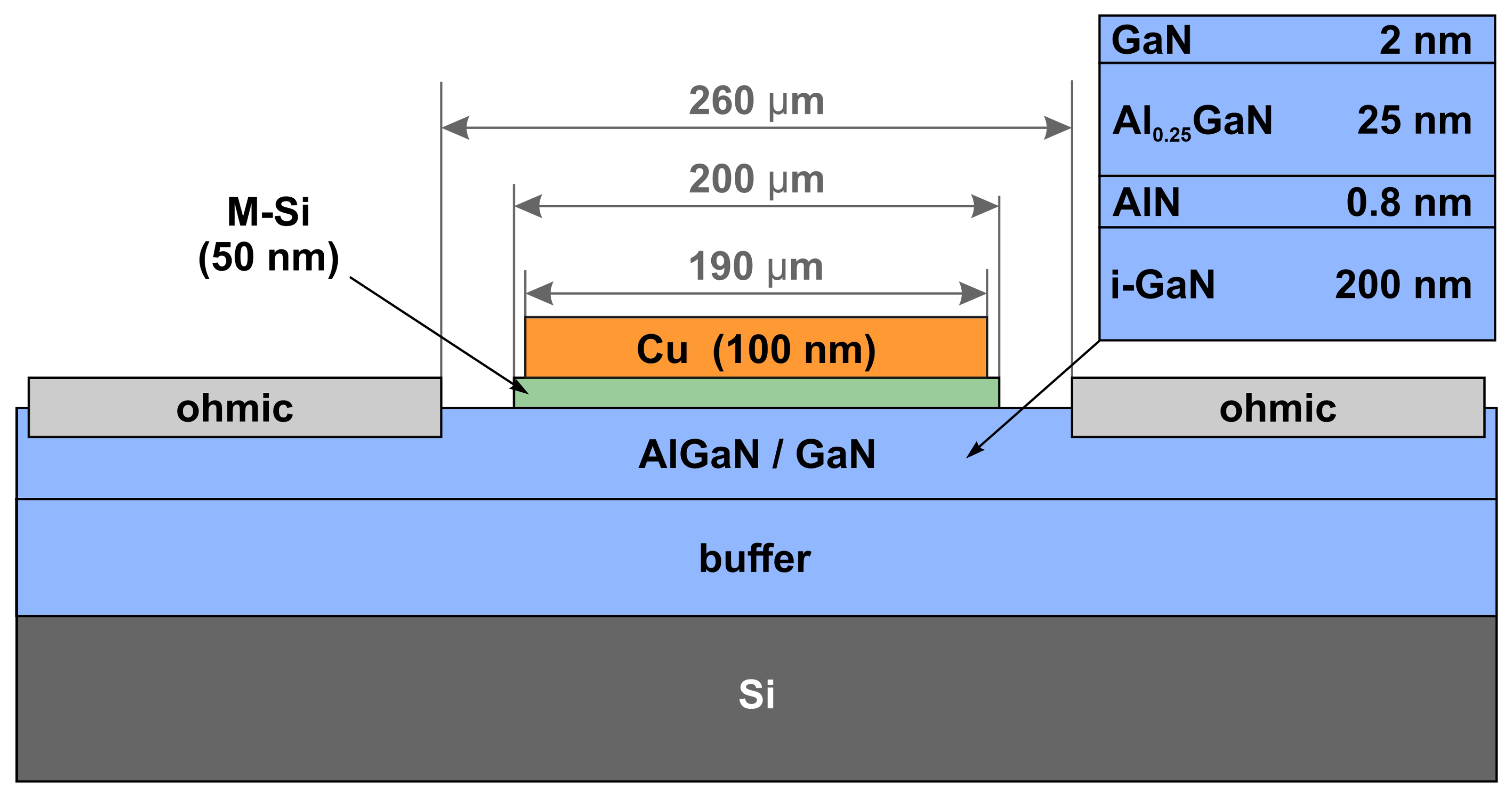
2. Materials and Methods

Metal–silicon (M–Si) layers were deposited at room temperature using DC magnetron sputtering (pAr = 1 × 10⁻² mbar) from stoichiometric targets, including TiSi2, TaSi2, CoSi2, Ni2Si, Pd2Si, IrSi, and Pt2Si. The microstructural properties of sputtered Pd–Si layers were investigated in [32], which clearly confirmed the Pd2Si composition of the layers. The compositions of the remaining layers will be generally referred to as M–Si compositions throughout the text. To eliminate the exact composition values from the discussion of the results, the work functions of the fabricated layers were determined through IPS measurements. Dedicated M–Si/SiO2/Si structures were fabricated for this purpose, including Ti–Si, Ta–Si, Co–Si, and Ni–Si layers. The patterns of M–Si circular pads (1 mm in diameter) were fabricated on thermally oxidized Si substrates using photolithography. After deposition, the structures were subjected to Rapid Thermal Processing (RTP) for 30 min at 300 °C under N2 atmosphere. The IPS optical system included an Xe 450 W lamp and a monochromator. The semi-transparent M–Si pads were illuminated, and the resulting photocurrents were measured for various wavelengths and applied voltages. Further details of the IPS experiment can be found in our previous report [32], which presents the results for the Pd2Si layer. The results for the sputtered IrSi can be found in [33].
Schottky planar diodes were fabricated on a commercially available GaN-cap/AlGaN/AlN-spacer/GaN-on-Si HEMT heterostructure. The wafer was cut into 1 cm² samples. All devices studied in this work were fabricated on samples originating from the same wafer. The layout of the device and details related to the heterostructure are shown in Figure 1. The diodes were fabricated using photolithography and consisted of a circular anode surrounded by a ring-shaped ohmic contact. The fabrication procedure began with surface preparation, which included cleaning with organic solutions and subsequent treatment with NH3: H2O2: H2O (1:1:5) and HCl: H2O (1:1). The ohmic contacts were then prepared and subjected to RTP at 750 °C. The devices differed in terms of the composition and preparation details of Schottky anodes. In addition to metal–silicide-based devices, diodes with Au/Ni or pure Cu anodes were fabricated. In the case of Pd2Si, Ir–Si, Pt–Si, and Ni layers, in situ Ar+ treatment (−300 V, 30 s) was applied directly before deposition. The layers were deposited in a manner similar to the corresponding layers in the IPS structures, i.e., using single, stoichiometric targets. After the deposition of the first layer in the anode stack (M–Si or Ni), but before the deposition of the overlayer (Cu or Au), some of the devices were subjected to RTP in N2 ambient at various temperatures ranging from 300 °C to 600 °C. Such annealing can be referred to as post-anode annealing or post-gate annealing (PGA). The influence of PGA on the electrical properties of Cu/Pd2Si Schottky contacts has been discussed in [29].
The current–voltage (IV) characteristics of the diodes were measured using an Agilent B1500 analyzer and a Cascade Summit 12,000 AP probe station. The thermal stability of the selected devices was evaluated by subjecting the diodes to subsequent annealing steps in vacuum at incremental temperatures ranging from 500 °C to 900 °C. High temperatures were applied to induce temperature-dependent changes within an acceptable period of time. Each annealing step took 6 h, with the exception of annealing at 900 °C, which lasted 3 h. The IV characteristics were measured after each annealing process. A study on the thermal stability of Cu/Pd2Si contacts, including microstructural characterization and comparison with the reference Au/Ni and Cu anodes, was reported in [14].

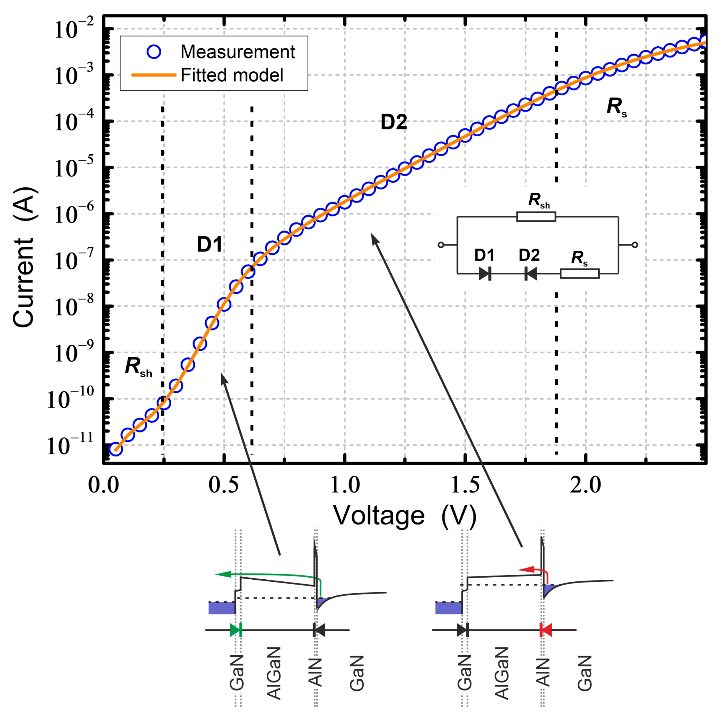
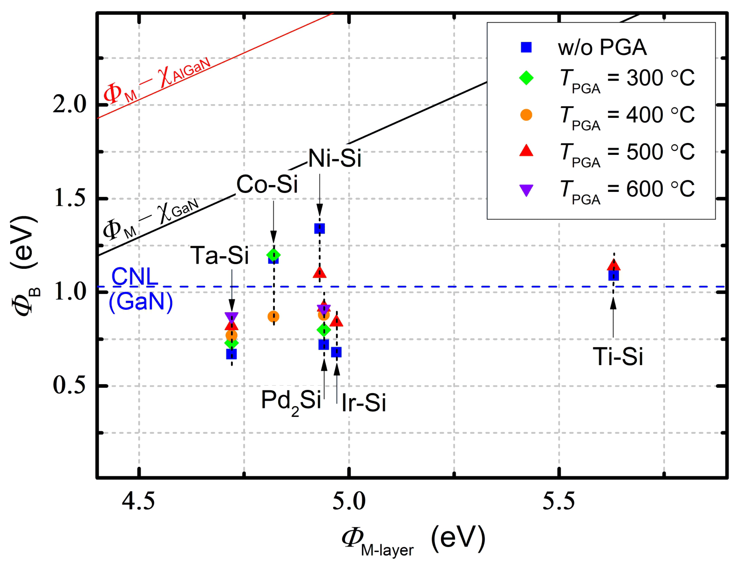
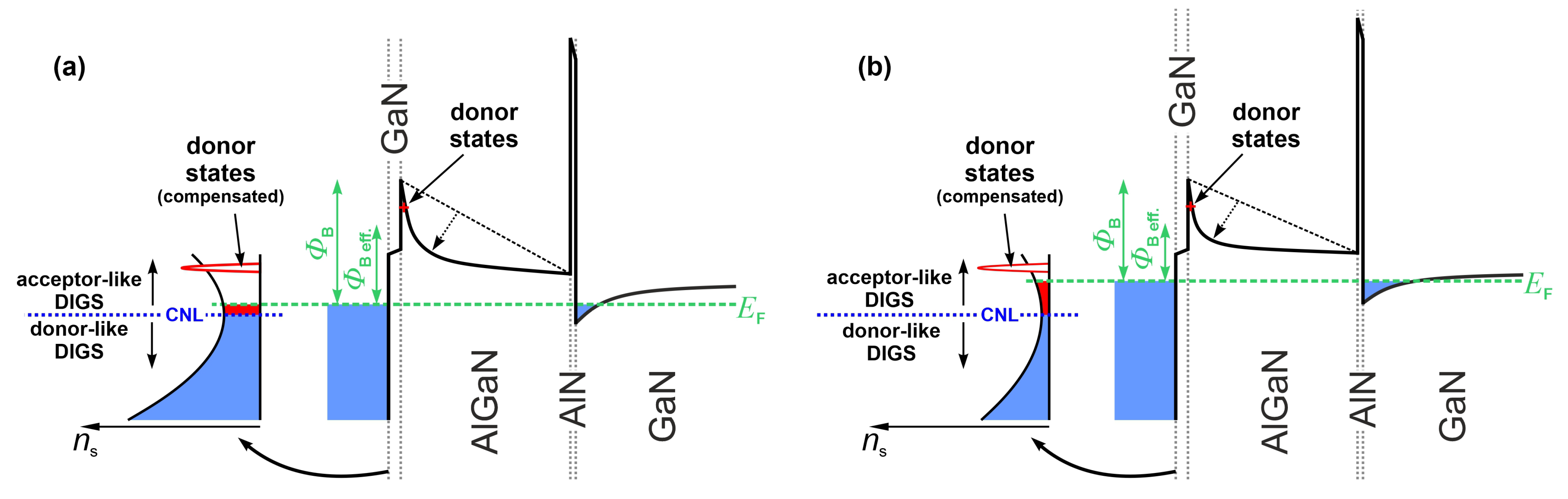
3. Results and Discussion

According to the Schottky–Mott rule [34], the expected height of the barrier formed at a metal–semiconductor junction is proportional to the work function of the metal. However, this rule does not apply if additional factors, such as interface states leading to Fermi level pinning, affect barrier formation. Therefore, the experimentally derived relationship between the barrier height and work function can provide initial insight into the formation mechanism of the Schottky barrier in the investigated structures. In this study, the work functions of the deposited layers ( Φ M-layer) were determined through IPS measurements.
The results are summarized in Table 1. The work functions measured for the prepared layers closely matched those expected for bulk materials with stoichiometries equal to those of the sputtering targets. The exception was the Ti–Si layer, for which the measured work function was significantly higher. This difference may be related to the exact stoichiometry or microstructure of the deposited Ti–Si layers.
To examine the electrical properties of metal–silicide Schottky contacts to the AlGaN/GaN heterostructure, planar diodes were fabricated according to the diagram shown in Figure 1. All forward IV characteristics measured on the diodes (including the reference Au/Ni and Cu diodes) had a characteristic form, showing two linear regions on a semi-logarithmic plot. A typical curve is shown in Figure 2. The linear regions are denoted as D1 and D2. The adaptation of the two-diodes model [35,36,37,38,39] can explain the observed IV relationships, as described in [29]. According to this model, the presence of the D1 area reflects the actual Schottky contact between the substrate and silicide (alternatively, with the Cu or Au/Ni anodes in the reference diodes). This is depicted in the band diagram in the inset at the bottom-left side of Figure 2. The D2 range is related to the heterostructure details. The interface between the GaN channel and AlGaN barrier, with a thin AlN spacing layer, limits the current flow at increased voltages. The band diagram at the bottom-right side of Figure 2 shows that electrons must overcome the barrier and tunnel through the barrier associated with the thin AlN layer. This can be modeled as a reverse-biased diode connected in series with the actual Schottky contact. Finally, at high voltages the series resistance (RS) limits the current, whereas at low voltages, the shunt current (∝ 1/Rsh) becomes dominant. The investigations on diodes with Cu/Pd2Si anodes indicated that the shunt component is likely caused by lateral leakage, assisted by surface states between the electrodes [29]. The properties of the actual Schottky contact are exposed only in a narrow voltage range (D1). The simple fitting of a straight line can be ambiguous, depending on the selected data points. Therefore, a more extensive analysis of the data points is advisable. The equivalent circuit of the model is shown in the inset of Figure 2. The RS can be omitted if the voltage range is limited to Rsh, D1, and D2. The parameters of the model, including the saturation current (IS) and ideality factor (n) of D1 diode, can be obtained by fitting the model to the experimental IV data. The Schottky barrier height can then be calculated from the IS using the thermionic emission model. The fitting procedure is described in detail in [29].
The forward and reverse IV characteristics of the diodes with various Cu/M–Si anodes are shown in Figure 3. For comparison, the results for the reference Au/Ni diode are also shown (dashed lines). Measurements of the pure Cu contacts can be found in [14]. The curves presented in Figure 3 were measured on diodes fabricated with PGA at 500 °C with the exception of diodes containing Co–Si or Ni–Si layers, which were fabricated without PGA. Unlike the other cases, the Co–Si and Ni–Si diodes exhibited higher Schottky barriers and lower leakage currents when no PGA was applied. It should also be noted that in the case of Pt–Si, only the diode with PGA was investigated.
To evaluate the Schottky contacts, the two-diodes model was fitted to the experimental data shown in Figure 3a. The fitted parameters, which include saturation currents and ideality factors of the D1 and D2 diodes, are listed in Table 2. The barrier heights, Φ B of the D1 diode in the model, relating to the M–Si/heterostructure interface, and Φ 2(0) relating to the AlGaN/AlN/GaN interfaces (at zero voltage), were calculated assuming the thermionic emission model. The theoretical values of the Richardson constant (32.5 A· cm−2 · K−2 for AlGAN and 24 A · cm−2 · K−2 for GaN) were used for these calculations. However, it should be noted that high ideality factors (n), which are commonly observed for AlGaN/GaN heterostructures, indicate that pure thermionic emission might not be sufficient to describe the forward conduction. The reverse current densities (Ir) measured at −10 V are also listed in Table 2.
In the literature, a broad range of leakage current values can be found for Schottky contacts to AlGaN/GaN heterostructures. Commonly, the reported reverse current density is in the range of 10−3 to above 10−2 A/cm² [7,25,26,27,28,40,41]. Some results show leakage close to 10−5 A/cm² [8] or 10−6 A/cm² [42]. The value of leakage current in most of the contacts investigated in this work falls within a typical range. The exceptionally good parameters were observed for diodes with Ti–Si and Ni–Si layers. However, comparing literature data can be challenging due to differences in substrates, details of the AlGaN/GaN heterostructure, or the geometry of the gate/anode (edge-to-area ratio). In this context, comparisons made with reference to a common Au/Ni stack can be helpful. Both Ni–Si and Ti–Si contacts showed lower leakage currents than the reference Au/Ni contact. This is consistent with the results reported in [7], where a Cu/TiSi2 Schottky contact to a similar heterostructure exhibited a better performance than an Au/Ni stack. Furthermore, the barrier extracted in this study for the Ti–Si-based contact fabricated without PGA, equal to 1.09 eV, is in very good agreement with the value 1.07 eV reported in [7]. The remaining five Cu/M–Si contacts exhibited higher leakage currents than Au/Ni with the highest values observed for Ta–Si.
Differences in the forward IV curves can also be noticed within the D2 voltage range. Various slopes of of the curves are visible, as evidenced by significant differences in n2 values listed in Table 2. According to the two-diodes model (Figure 2), the current flow in this range is dictated by the properties of the AlGaN/AlN-spacer/GaN interfaces. Chen et al. [38] experimentally demonstrated that D2 range depends on the thickness of the AlN spacer layer. One could speculate that variations in the microstructural properties of the AlN interlayer are responsible for the observed differences. However, in this work, significant variations in the heterostructure are not expected, since all devices were fabricated using samples from the same wafer. Another possible origin of the observed differences is proposed at the end of this section. On the other hand, the range of observed values of Φ 2(0) (0.52–0.58 eV) is relatively narrow, as expected. Presumably, the observed differences can be explained by the inhomogeneities of the wafer.
In Figure 4, the work functions measured by the IPS method (Table 1) are compared with the Schottky barrier heights determined by fitting the model to the experimental IV curves. The Schottky barrier heights were determined for the diodes fabricated under various PGA conditions. As already mentioned, the impact of PGA on the electrical properties of the diodes varied depending on the silicide applied. The solid lines plotted in the figure describe the expected dependence of the barrier height on the work function according to the Schottky–Mott rule for GaN and Al0.25Ga0.75N, assuming electron affinity values from the literature [43]. However, no clear relationship was observed between the experimental values. It can be concluded that the barrier height is mainly affected by the details of the technological process, such as the PGA conditions, and not by the work function. Moreover, it can be noticed that the measured barrier heights are comparable to the CNL (Charge Neutrality Level) for GaN [44], which is marked by the dashed line in Figure 4. According to the DIGS (Disorder Induced Gap States) model [44], the interface states above the CNL are acceptor-like and the states below the CNL are donor-like. The CNL may cause pinning of the Fermi level, making the Schottky barrier height independent of the metal work function. Schottky barrier formation is discussed later in this article.
To test the thermal stability, selected samples with diodes were subjected to subsequent annealing processes in vacuum, at incremental temperatures ranging from 500 °C to 900 °C. Diodes with Co–Si or Ta–Si layers were excluded from the tests because of the relatively weak performance of the as-prepared devices. Namely, the barrier height in the Co–Si diodes dropped significantly owing to the application of PGA, even when a temperature as low as 400 °C was applied during preparation (Figure 4). The Ta–Si devices were characterized by high leakage currents (2.6 × 10⁻¹ A/cm2 in the diode without PGA), which were the highest regardless of the PGA applied during preparation (Figure 3b). The devices selected for the tests are indicated on the horizontal axes of Figure 5 by descriptions of the materials applied in the anodes. The good resilience of the devices to high temperatures forced the use of high temperatures to observe temperature-related changes within an acceptable time. Each annealing process lasted 6 h, except for annealing at 900 °C, which lasted for 3 h. After each annealing, the IV characteristics were measured using the same selected devices. The diodes were subjected to subsequent annealing steps either until a temperature of 900 °C was reached, or the parameters of the tested devices significantly deteriorated. The results are summarized in Figure 5a (leakage currents measured at −10 V) and Figure 5b (barrier heights). The arrangements of the data on the horizontal axes in Figure 5a,b are identical and correspond to the maximum leakage current observed at any stage of the test. The diodes with the highest (worst) leakage current values are placed on the left side.
As shown in Figure 5a, the reference diode with a Cu anode was characterized by the highest leakage, which increased significantly after annealing at 700 °C. Because of the high leakage current, the diode was not subjected to further annealing steps. The next reference diode, that is, the one with Au/Ni anode, had a relatively low leakage current before annealing. However, during the thermal tests, the current increased by approximately two orders of magnitude, placing the Au/Ni diode close to the Cu diode in Figure 5. After completing the tests, all the tested diodes with a silicide layer were characterized by lower (better) leakage currents than those of the reference Au/Ni and Cu diodes. The lowest leakage currents before annealing were observed for Cu/Ti–Si and Cu/Ni–Si (fabricated without PGA). The Ni–Si diode fabricated without PGA had the highest Schottky barrier during all stages of the test (Figure 5b). Despite the significant relative differences in the values measured on this diode after the subsequent stages, the final leakage current was the lowest compared with the other structures (Figure 5a). The smallest relative differences between the measured values were observed for the Pd2Si diodes. The exceptional thermal stability of Pd2Si diodes was discussed in [14]. As shown in Figure 5, the Pt–Si diode also exhibited small relative differences in the extracted parameters.
Figure 6 combines all the measurements discussed in this study to display the ideality factors and leakage currents vs. barrier heights. The ideality factors (Figure 6a) oscillate in a wide range, and no clear relationship with the barrier height can be observed. The reverse current (measured at −10 V) exhibited a declining trend with increasing barrier height when displayed on a semi-logarithmic plot (Figure 6b). However, the scatter of the values is considerably large. The leakage currents can differ by a few orders of magnitude for diodes with similar barrier heights. Various mechanisms can contribute to the reverse current in Schottky contacts to AlGaN/GaN heterostructures [45,46], but the leakage is usually linked to some type of defects. Therefore, the broad range of measured values indicates complex interfacial phenomena, leading to variable densities of defects and electronic states near the interface.
An important factor that can influence electrical conduction is related to extended defects, which are typically introduced during epitaxial growth in lattice-mismatched systems [47,48]. The presence of threading dislocations in heteroepitaxial structures causes a local lowering of the Schottky barrier and may result in the formation of preferential current conduction paths [49]. This is particularly important for the generation of leakage current or the presence of electrically active states in the band gap. In the case of the structures investigated in this study, the effects of Schottky barrier inhomogeneity on forward conduction were observed at lowered temperatures. Forward IV measurements performed at various temperatures for Cu/Pd2Si contacts have shown that the effect of inhomogeneities becomes significant only below room temperature [29]. Furthermore, all investigated devices were fabricated on samples cut from the same wafer, so similar densities of extended defects are expected.
The following model is proposed to describe the complex phenomena leading to the formation of a Schottky barrier in the investigated diodes. As already pointed out, the Schottky barrier heights in the investigated diodes are not dependent on the work function of the M–Si layer. This observation can be explained by pinning of the Fermi level. According to the DIGS model [44], the atomic disorder at the metal/(Al)GaN interface introduces a continuous distribution of states energetically located in the band gap. Pinning occurs at the CNL, that is, at the energy level that separates the acceptor-like and donor-like DIGS. However, this does not explain the broad range of barrier heights observed in this study (Figure 4 and Figure 5b) and additional phenomena should be considered.
A schematic of the proposed explanation is presented in Figure 7. The figure shows two band diagrams, where the effective barrier for electrons in Figure 7a is higher than that in Figure 7b. The densities of the band gap states (ns), which are spatially located at the M–Si/GaN-cap interface, are shown in the insets of Figure 7a,b. Beside the DIGS, discrete donor states related to nitrogen vacancies and their complexes are commonly observed in GaN [50,51,52,53,54]. Unlike the deeper, donor-like DIGS, these donor states are ionized and are represented by red lines in the insets of Figure 7a,b. The model assumes that the pinning of the Fermi level (green, dashed lines) can change its position on the energy scale (vertical axis), depending on the ratio of the density of ionized donor states to the density of the DIGS. When the densities of DIGS are relatively high (Figure 7a), the Fermi level is pinned close to the original CNL because only a small shift of the Fermi level toward the acceptor-like states is sufficient to maintain charge neutrality. The acceptor-like states below the Fermi level become ionized (marked in red in the insets of Figure 7) and compensate for the charge related to the ionized donor states. When the DIGS densities are relatively low compared with the ionized donor states (Figure 7b), a larger Fermi level shift toward an acceptor-like DIGS is necessary to compensate for the positive charge. Thus, the barrier ΦB in Figure 7b is lower than that in Figure 7a.
Assuming that Fermi level pinning is caused by the electronic states at the interface with the GaN cap, the barrier Φ B in Figure 7 should be larger than the GaN/AlGaN conduction-band offset, that is, larger than (according to Anderson’s rule), the difference between the electron affinity of GaN and Al0.25Ga0.75N (approximately 0.73 eV [43]). However, in a few cases in this study, the observed barrier heights were lower than 0.73 eV (Figure 4). The lowest barrier height was equal to 0.67 eV and was observed for the as-prepared diode with Cu/Ta–Si anode, fabricated without PGA. Therefore, unless the actual band offset is distinctly smaller than assumed (which is also possible [55]), the forward conduction process likely involves tunneling through the AlGaN barrier. The assumption of tunneling aligns with the conclusions drawn from the discussion of forward and reverse currents in Cu/Pd2Si diodes, as presented in [29]. This is further supported by the observed ideality factors, which are significantly higher than 1 (Figure 6a), indicating mechanisms other than the pure thermionic emission. Tunneling through AlGaN can be explained using Thermionic Field Emission (TFE) and Thin Surface Barrier (TSB) models [44,56]. In the discussed case, the AlGaN layer is covered with a thin GaN capping layer. Because the GaN-cap/AlGaN interface is epitaxial, the DIGS are not expected to occur. Therefore, the positive charges related to the donor states, spatially located in the vicinity of the Gan-cap/AlGaN interface, are not compensated. According to the TSB model [44,56], positive charges near the surface produce thin-surface-barrier regions. This is schematically shown in Figure 7a,b, where the original conduction band edge for AlGaN is depicted by the dashed black lines. The unintentional donor states are likely introduced during device processing [56]. This assumptions is supported by the results and discussion on the effects of PGA annealing on Cu/Pd2Si diodes presented in [29]. The thinned barrier allows the TFE to contribute to the conduction mechanism. Consequently, the measured effective barrier height ( Φ B eff. in Figure 7) is lower than the actual barrier height Φ B.
The model explains the complex behavior of the investigated diodes. According to the model, the barrier height is independent of the work function, which agrees with the experimental results. It is determined by the density of unintentional donor states and the relative density of the DIGS at the M–Si/GaN-cap interface. Depending on the applied M–Si layer, various atomic arrangements are formed at the interface, which affects the DIGS. This could explain why diodes fabricated with the same technological procedure, but with various metal silicides, can reveal different barrier heights. It can also be expected that the fabrication details (surface preparation, sputtering, PGA, etc.) affect both the atomic ordering at the interface (and therefore, the DIGS) and the distribution of unintentional donor defects near the surface of the heterostructure. Hence, various barrier heights were obtained for a given M–Si layer (Figure 4). Similarly, the effect of annealing can differ depending on the M–Si layer and the fabrication details of the device.
Based on the model, it is also possible to speculate on the cause of the various slopes in IV curves observed in the D2 voltage range (Figure 3). The insets in Figure 2 illustrate electron transport in D1 and D2 voltage regimes assuming tunneling through AlN and pure thermionic emission over the AlGaN barrier. According to the model from Figure 7, the latter assumption is not valid. Instead, the electrons will tunnel through the AlGaN barrier in TSB regions for both D1 and D2 voltage ranges. Therefore, the current flow in the D2 range is also affected by the density of unintentional donors near the GaN-cap/AlGaN interface. Assuming a thermionic field emission process through a TSB, the ideality factor should increase with the density of unintentional donors [44]. Thus, it can be implied that the different slopes in the D2 range (n2) may result from various densities of electrically active defects near the GaN-cap/AlGaN interface. As mentioned before, high densities of unintentional donors should result in a TSB and a lowering of the measured barrier ( Φ B in Table 2). Therefore, in general, high values of n2 should be accompanied by relatively low ΦB. This is supported by the values listed in Table 2. For the diodes with n2 in the range 3.91–6.66, relatively low effective barriers (<1 eV) were observed, while for the diodes with n2 in the range 2.76–3.6, higher barriers (>1 eV) were extracted.
The question remains: what could be the source of different defect densities near the GaN-cap/AlGaN interface in devices differing only in the applied M–Si layer? As suggested in [56], during the deposition of a layer, the bombardment of the surface by atoms may produce defects, such as nitrogen vacancies, that can be responsible for the formation of a TSB. On the other hand, the energies of sputtered atoms depend on various factors, including atom mass and surface binding energy. The simulations reported in [57] have shown that the energies of atoms sputtered from single-element materials vary depending on the position of the element in the periodic table, including the group and period. Thus, it is expected that the energies of atoms sputtered from various metal silicide targets will differ, resulting in different densities and depth distributions of defects generated in the near-surface regions of the heterostructure, including the GaN-cap/AlGaN interface. This could explain the various n2 values observed in this study.

4. Summary and Conclusions

The Schottky barrier heights in the planar diodes with Cu/M–Si/heterostructure contacts did not depend on the M–Si layer work function. The barriers were strongly dependent on the parameters of the fabrication process and on the choice of metal silicide. The highest Schottky barriers were obtained for the diodes with Cu/Ni–Si (up to 1.34 eV) and Cu/Ti–Si (up to 1.14 eV) anodes. These diodes also exhibited lower leakage currents than the reference Au/Ni diode. The diodes with Cu/Co–Si anodes exhibited high barriers, but with considerably high leakage currents, and were susceptible to annealing. Their electrical performance deteriorated when annealing above 300 °C was applied during fabrication.
During the thermal stability tests, the barrier height of the diode containing Ni–Si gradually worsened after each annealing, but were always better than those in all other measured devices (including the as-prepared diodes) even after the final annealing at 900 °C. The diodes with Pd–Si or Pt–Si layers exhibited exceptionally small relative differences in the extracted parameters measured after subsequent annealing steps. After completion of the tests, all tested diodes with M–Si layers (Ni–Si, Pd–Si, Ir–Si, Ti–Si, or Pt–Si) had lower leakage currents than the reference Au/Ni diode.
The mechanism for Schottky barrier formation was proposed to explain the complex behavior of the investigated diodes. The mechanism is based on the unified DIGS and TSB models [44] and assumes the pinning of the Fermi level at the M–Si/GaN-cap interface. It also incorporates a pinning shift that depends on the ratio of the donor to acceptor-like band gap states densities.
It can be concluded that Au-free Schottky contacts based on specific M–Si layers exhibit the performance that is very promising for applications in GaN-on-Si HEMTs. The thermal stability of the diodes with Cu/M–Si anode stack was greatly improved compared to that of the devices with the single-layer Cu contact. The parameters of some metal–silicide-based devices exceeded those of the reference Au/Ni Schottky diode. Optimizing the stoichiometry and fabrication processes of specific M–Si layers could lead to further improvements.

Author Contributions

Conceptualization, M.W.; methodology, M.W., M.E., K.P., E.B. and A.T.; formal analysis, M.W. and K.P.; investigation, M.W., K.P., M.A.B. and E.B.; resources, M.E. and J.T.; writing—original draft preparation, M.W.; writing—review and editing, K.P. and A.T.; visualization, M.W.; project administration, M.W.; funding acquisition, M.W. All authors have read and agreed to the published version of the manuscript.

Funding

This research was funded by the National Science Centre, Poland, grant no. 2018/31/D/ST7/02901.

Data Availability Statement

Dataset is available on reasonable request from the corresponding author.

Conflicts of Interest

The authors declare no conflicts of interest.

References

  1. Buffolo, M.; Favero, D.; Marcuzzi, A.; De Santi, C.; Meneghesso, G.; Zanoni, E.; Meneghini, M. Review and Outlook on GaN and SiC Power Devices: Industrial State-of-the-Art, Applications, and Perspectives. IEEE Trans. Electron Devices 2024, 71, 1344–1355. [Google Scholar] [CrossRef]
  2. Chen, K.J.; Häberlen, O.; Lidow, A.; Tsai, C.L.; Ueda, T.; Uemoto, Y.; Wu, Y. GaN-on-Si Power Technology: Devices and Applications. IEEE Trans. Electron Devices 2017, 64, 779–795. [Google Scholar] [CrossRef]
  3. Liu, Z.; Sun, M.; Lee, H.S.; Heuken, M.; Palacios, T. AlGaN/AlN/GaN High-Electron-Mobility Transistors Fabricated with Au-Free Technology. Appl. Phys. Express 2013, 6, 096502. [Google Scholar] [CrossRef]
  4. Arulkumaran, S.; Ng, G.I.; Vicknesh, S.; Wang, H.; Ang, K.S.; Kumar, C.M.; Teo, K.L.; Ranjan, K. Demonstration of Submicron-Gate AlGaN/GaN High-Electron-Mobility Transistors on Silicon with Complementary Metal–Oxide–Semiconductor-Compatible Non-Gold Metal Stack. Appl. Phys. Express 2012, 6, 016501. [Google Scholar] [CrossRef]
  5. Tham, W.H.; Bera, L.K.; Ang, D.S.; Dolmanan, S.B.; Bhat, T.N.; Tripathy, S. AlxGa1-xN/GaN MISHEMTs with a Common Gold-Free Metal-Stack for Source/Drain/Gate. IEEE Electron Device Lett. 2015, 36, 1291–1294. [Google Scholar] [CrossRef]
  6. Li, Y.; Ng, G.I.; Arulkumaran, S.; Liu, Z.H.; Ranjan, K.; Xing, W.C.; Ang, K.S.; Murmu, P.P.; Kennedy, J. AlGaN/GaN high electron mobility transistors on Si with sputtered TiN gate. Phys. Status Solidi (a) 2017, 214, 1600555. [Google Scholar] [CrossRef]
  7. Yoon, S.; Lee, S.M.; Kim, J.; Lee, H.D.; Cha, H.Y.; Oh, J. Evaluation of titanium disilicide/copper Schottky gate for AlGaN/GaN high electron mobility transistors. Semicond. Sci. Technol. 2017, 32, 035012. [Google Scholar] [CrossRef]
  8. Greco, G.; Franco, S.D.; Bongiorno, C.; Grzanka, E.; Leszczynski, M.; Giannazzo, F.; Roccaforte, F. Thermal annealing effect on electrical and structural properties of Tungsten Carbide Schottky contacts on AlGaN/GaN heterostructures. Semicond. Sci. Technol. 2020, 35, 105004. [Google Scholar] [CrossRef]
  9. Garg, M.; Kumar, A.; Sun, H.; Liao, C.H.; Li, X.; Singh, R. Temperature dependent electrical studies on Cu/AlGaN/GaN Schottky barrier diodes with its microstructural characterization. J. Alloy. Compd. 2019, 806, 852–857. [Google Scholar] [CrossRef]
  10. Ao, J.P.; Kikuta, D.; Kubota, N.; Naoi, Y.; Ohno, Y. Copper gate AlGaN/GaN HEMT with low gate leakage current. IEEE Electron Device Lett. 2003, 24, 500–502. [Google Scholar] [CrossRef]
  11. Sun, H.F.; Alt, A.R.; Bolognesi, C.R. Submicrometer Copper T-Gate AlGaN/GaN HFETs: The Gate Metal Stack Effect. IEEE Electron Device Lett. 2007, 28, 350–353. [Google Scholar] [CrossRef]
  12. Esposto, M.; Lecce, V.D.; Bonaiuti, M.; Chini, A. The Influence of Interface States at the Schottky Junction on the Large Signal Behavior of Copper-Gate GaN HEMTs. J. Electron. Mater. 2013, 42, 15–20. [Google Scholar] [CrossRef]
  13. Park, J.; Lee, K.; Cha, H.Y.; Seo, K. Thermal instability of copper gate AlGaN/GaN HEMT on Si substrate. Electron. Lett. 2010, 46, 1011–1012. [Google Scholar] [CrossRef]
  14. Wzorek, M.; Ekielski, M.; Tarenko, J.; Borysiewicz, M.A.; Brzozowski, E.; Taube, A. Thermal Stability of Cu/Pd2Si/, Cu/, and Au/Ni/ Schottky Contacts to AlGaN/GaN Heterostructures. IEEE Trans. Electron Devices 2024, 71, 490–495. [Google Scholar] [CrossRef]
  15. Tallarico, A.N.; Stoffels, S.; Magnone, P.; Hu, J.; Lenci, S.; Marcon, D.; Sangiorgi, E.; Fiegna, C.; Decoutere, S. Reliability of Au-Free AlGaN/GaN-on-Silicon Schottky Barrier Diodes Under ON-State Stress. IEEE Trans. Electron Devices 2016, 63, 723–730. [Google Scholar] [CrossRef]
  16. Hu, J.; Stoffels, S.; Lenci, S.; Bakeroot, B.; De Jaeger, B.; Van Hove, M.; Ronchi, N.; Venegas, R.; Liang, H.; Zhao, M.; et al. Performance Optimization of Au-Free Lateral AlGaN/GaN Schottky Barrier Diode with Gated Edge Termination on 200-mm Silicon Substrate. IEEE Trans. Electron Devices 2016, 63, 997–1004. [Google Scholar] [CrossRef]
  17. Acurio, E.; Trojman, L.; Crupi, F.; Moposita, T.; De Jaeger, B.; Decoutere, S. Reliability Assessment of AlGaN/GaN Schottky Barrier Diodes Under ON-State Stress. IEEE Trans. Device Mater. Reliab. 2020, 20, 167–171. [Google Scholar] [CrossRef]
  18. Sun, H.; Liu, M.; Liu, P.; Lin, X.; Chen, J.; Wang, M.; Chen, D. Optimization of Au-Free Ohmic Contact Based on the Gate-First Double-Metal AlGaN/GaN MIS-HEMTs and SBDs Process. IEEE Trans. Electron Devices 2018, 65, 622–628. [Google Scholar] [CrossRef]
  19. Chen, Y.C.; Tang, S.W.; Lin, P.H.; Chen, Z.C.; Lu, M.H.; Kao, K.H.; Wu, T.L. Silicon Nitride-induced Threshold Voltage Shift in p-GaN HEMTs with Au-free Gate-first Process. In Proceedings of the 2020 IEEE International Symposium on the Physical and Failure Analysis of Integrated Circuits (IPFA), Singapore, 20–23 July 2020; pp. 1–5. [Google Scholar] [CrossRef]
  20. Lenci, S.; De Jaeger, B.; Carbonell, L.; Hu, J.; Mannaert, G.; Wellekens, D.; You, S.; Bakeroot, B.; Decoutere, S. Au-Free AlGaN/GaN Power Diode on 8-in Si Substrate with Gated Edge Termination. IEEE Electron Device Lett. 2013, 34, 1035–1037. [Google Scholar] [CrossRef]
  21. Hu, J.; Stoffels, S.; Lenci, S.; Wu, T.L.; Ronchi, N.; You, S.; Bakeroot, B.; Groeseneken, G.; Decoutere, S. Investigation of constant voltage off-state stress on Au-free AlGaN/GaN Schottky barrier diodes. Jpn. J. Appl. Phys. 2015, 54, 04DF07. [Google Scholar] [CrossRef]
  22. Hu, J.; Stoffels, S.; Lenci, S.; Bakeroot, B.; Venegas, R.; Groeseneken, G.; Decoutere, S. Current transient spectroscopy for trapping analysis on Au-free AlGaN/GaN Schottky barrier diode. Appl. Phys. Lett. 2015, 106, 083502. [Google Scholar] [CrossRef]
  23. Posthuma, N.E.; You, S.; Stoffels, S.; Wellekens, D.; Liang, H.; Zhao, M.; De Jaeger, B.; Geens, K.; Ronchi, N.; Decoutere, S.; et al. An industry-ready 200 mm p-GaN E-mode GaN-on-Si power technology. In Proceedings of the 2018 IEEE 30th International Symposium on Power Semiconductor Devices and ICs (ISPSD), Chicago, IL, USA, 13–17 May 2018; pp. 284–287. [Google Scholar] [CrossRef]
  24. Ao, J.P.; Naoi, Y.; Ohno, Y. Thermally stable TiN Schottky contact on AlGaN/GaN heterostructure. Vacuum 2013, 87, 150–154. [Google Scholar] [CrossRef]
  25. Wu, Y.; Zhang, W.; Zhang, J.; Zhao, S.; Luo, J.; Tan, X.; Mao, W.; Zhang, C.; Zhang, Y.; Cheng, K.; et al. Au-Free Al0.4Ga0.6N/Al0.1Ga0.9N HEMTs on Silicon Substrate with High Reverse Blocking Voltage of 2 kV. IEEE Trans. Electron Devices 2021, 68, 4543–4549. [Google Scholar] [CrossRef]
  26. Niranjan, S.; Rao, A.; Muralidharan, R.; Sen, P.; Nath, D.N. Performance Comparison of Au-Based and Au-Free AlGaN/GaN HEMT on Silicon. IEEE Trans. Electron Devices 2022, 69, 1014–1019. [Google Scholar] [CrossRef]
  27. Fontserè, A.; Pérez-Tomás, A.; Banu, V.; Godignon, P.; Millán, J.; De Vleeschouwer, H.; Parsey, J.M.; Moens, P. A HfO2 based 800 V/300 °C Au-free AlGaN/GaN-on-Si HEMT technology. In Proceedings of the 2012 24th International Symposium on Power Semiconductor Devices and ICs, Bruges, Belgium, 3–7 June 2012; pp. 37–40. [Google Scholar] [CrossRef]
  28. Hsieh, T.E.; Lin, Y.C.; Chu, C.M.; Chuang, Y.L.; Huang, Y.X.; Shi, W.C.; Dee, C.F.; Majlis, B.Y.; Lee, W.I.; Chang, E.Y. Au-Free GaN High-Electron-Mobility Transistor with Ti/Al/W Ohmic and WNX Schottky Metal Structures for High-Power Applications. J. Electron. Mater. 2016, 45, 3285–3289. [Google Scholar] [CrossRef]
  29. Wzorek, M.; Ekielski, M.; Brzozowski, E.; Taube, A. Electrical properties of Cu/Pd2Si Schottky contacts to AlGaN/GaN-on-Si HEMT heterostructures. Mater. Sci. Semicond. Process. 2023, 153, 107157. [Google Scholar] [CrossRef]
  30. Kim, J.; Ren, F.; Baca, A.G.; Pearton, S.J. Thermal stability of WSix and W Schottky contacts on n-GaN. Appl. Phys. Lett. 2003, 82, 3263–3265. [Google Scholar] [CrossRef]
  31. Bucher, E.; Schulz, S.; Lux-Steiner, M.C.; Munz, P.; Gubler, U.; Greuter, F. Work function and barrier heights of transition metal silicides. Appl. Phys. A 1986, 40, 71–77. [Google Scholar] [CrossRef]
  32. Piskorski, K.; Wzorek, M.; Ekielski, M.; Dobrzański, L.; Gaca, J.; Malinowska, A.; Michałowski, P.; Borysiewicz, M. Photoelectric, optical and microstructural characterization of thin palladium silicide (Pd2Si) layers fabricated by magnetron sputtering from a stoichiometric target. Mater. Sci. Eng. B 2022, 283, 115831. [Google Scholar] [CrossRef]
  33. Taube, A.; Borysiewicz, M.A.; Sadowski, O.; Wójcicka, A.; Tarenko, J.; Piskorski, K.; Wzorek, M. Investigation of amorphous (Ir,Ru)-Si and (Ir,Ru)-Si-O Schottky contacts to (001) β-Ga2O3. Mater. Sci. Semicond. Process. 2023, 154, 107218. [Google Scholar] [CrossRef]
  34. Tung, R.T. The physics and chemistry of the Schottky barrier height. Appl. Phys. Rev. 2014, 1, 011304. [Google Scholar] [CrossRef]
  35. Chen, C.H.; Baier, S.; Arch, D.; Shur, M. A new and simple model for GaAs heterojunction FET gate characteristics. IEEE Trans. Electron Devices 1988, 35, 570–577. [Google Scholar] [CrossRef]
  36. Lv, Y.; Lin, Z.; Corrigan, T.D.; Zhao, J.; Cao, Z.; Meng, L.; Luan, C.; Wang, Z.; Chen, H. Extraction of AlGaN/GaN heterostructure Schottky diode barrier heights from forward current-voltage characteristics. J. Appl. Phys. 2011, 109, 074512. [Google Scholar] [CrossRef]
  37. Lü, Y.-J.; Feng, Z.-H.; Gu, G.-D.; Dun, S.-B.; Yin, J.-Y.; Han, T.-T.; Sheng, B.-C.; Cai, S.-J.; Liu, B.; Lin, Z.-J. Directly extracting both threshold voltage and series resistance from the conductance—Voltage curve of an AlGaN/GaN Schottky diode. Chin. Phys. B 2013, 22, 077102. [Google Scholar] [CrossRef]
  38. Chen, C.-h.; Wang, D.; Hou, D.; Yang, Y.; Yau, W.; Sadler, R.; Sutton, W.; Shim, J.; Wang, S. The Impact of AlN Spacer on Forward Gate Current and Stress-Induced Leakage Current (SILC) of GaN HEMT. In Proceedings of the 2016 IEEE Compound Semiconductor Integrated Circuit Symposium (CSICS), Austin, TX, USA, 23–26 October 2016; pp. 1–4. [Google Scholar] [CrossRef]
  39. Greco, G.; Giannazzo, F.; Roccaforte, F. Temperature dependent forward current-voltage characteristics of Ni/Au Schottky contacts on AlGaN/GaN heterostructures described by a two diodes model. J. Appl. Phys. 2017, 121, 045701. [Google Scholar] [CrossRef]
  40. Kim, H.; Schuette, M.; Jung, H.; Song, J.; Lee, J.; Lu, W.; Mabon, J.C. Passivation effects in Ni/AlGaN/GaN Schottky diodes by annealing. Appl. Phys. Lett. 2006, 89, 053516. [Google Scholar] [CrossRef]
  41. Persano, A.; Pio, I.; Tasco, V.; Cuscunà, M.; Passaseo, A.; Cola, A. Electrical properties of planar AlGaN/GaN Schottky diodes: Role of 2DEG and analysis of non-idealities. J. Appl. Phys. 2017, 121, 135701. [Google Scholar] [CrossRef]
  42. Jin Ha, W.; Chhajed, S.; Jae Oh, S.; Hwang, S.; Kyu Kim, J.; Lee, J.H.; Kim, K.S. Analysis of the reverse leakage current in AlGaN/GaN Schottky barrier diodes treated with fluorine plasma. Appl. Phys. Lett. 2012, 100, 132104. [Google Scholar] [CrossRef]
  43. Grabowski, S.P.; Schneider, M.; Nienhaus, H.; Mönch, W.; Dimitrov, R.; Ambacher, O.; Stutzmann, M. Electron affinity of AlxGa1-xN(0001) surfaces. Appl. Phys. Lett. 2001, 78, 2503–2505. [Google Scholar] [CrossRef]
  44. Hasegawa, H.; Inagaki, T.; Ootomo, S.; Hashizume, T. Mechanisms of current collapse and gate leakage currents in AlGaN/GaN heterostructure field effect transistors. J. Vac. Sci. Technol. B Microelectron. Nanometer Struct. Process. Meas. Phenom. 2003, 21, 1844–1855. [Google Scholar] [CrossRef]
  45. Yan, D.; Lu, H.; Cao, D.; Chen, D.; Zhang, R.; Zheng, Y. On the reverse gate leakage current of AlGaN/GaN high electron mobility transistors. Appl. Phys. Lett. 2010, 97, 153503. [Google Scholar] [CrossRef]
  46. Turuvekere, S.; Karumuri, N.; Rahman, A.A.; Bhattacharya, A.; DasGupta, A.; DasGupta, N. Gate Leakage Mechanisms in AlGaN/GaN and AlInN/GaN HEMTs: Comparison and Modeling. IEEE Trans. Electron Devices 2013, 60, 3157–3165. [Google Scholar] [CrossRef]
  47. Bae, S.H.; Lu, K.; Han, Y.; Kim, S.; Qiao, K.; Choi, C.; Nie, Y.; Kim, H.; Kum, H.S.; Chen, P.; et al. Graphene-assisted spontaneous relaxation towards dislocation-free heteroepitaxy. Nat. Nanotechnol. 2020, 15, 272–276. [Google Scholar] [CrossRef]
  48. Meng, Y.; Feng, J.; Han, S.; Xu, Z.; Mao, W.; Zhang, T.; Kim, J.S.; Roh, I.; Zhao, Y.; Kim, D.H.; et al. Photonic van der Waals integration from 2D materials to 3D nanomembranes. Nat. Rev. Mater. 2023, 8, 498–517. [Google Scholar] [CrossRef]
  49. Besendörfer, S.; Meissner, E.; Medjdoub, F.; Derluyn, J.; Friedrich, J.; Erlbacher, T. The impact of dislocations on AlGaN/GaN Schottky diodes and on gate failure of high electron mobility transistors. Sci. Rep. 2020, 10, 17252. [Google Scholar] [CrossRef]
  50. Chen, Y.; Haller, C.; Liu, W.; Karpov, S.Y.; Carlin, J.F.; Grandjean, N. GaN buffer growth temperature and efficiency of InGaN/GaN quantum wells: The critical role of nitrogen vacancies at the GaN surface. Appl. Phys. Lett. 2021, 118, 111102. [Google Scholar] [CrossRef]
  51. Lin, Y.J.; Ker, Q.; Ho, C.Y.; Chang, H.C.; Chien, F.T. Nitrogen-vacancy-related defects and Fermi level pinning in n-GaN Schottky diodes. J. Appl. Phys. 2003, 94, 1819–1822. [Google Scholar] [CrossRef]
  52. Hashizume, T.; Nakasaki, R. Discrete surface state related to nitrogen-vacancy defect on plasma-treated GaN surfaces. Appl. Phys. Lett. 2002, 80, 4564–4566. [Google Scholar] [CrossRef]
  53. Look, D.C.; Farlow, G.C.; Drevinsky, P.J.; Bliss, D.F.; Sizelove, J.R. On the nitrogen vacancy in GaN. Appl. Phys. Lett. 2003, 83, 3525–3527. [Google Scholar] [CrossRef]
  54. Schwarz, C.; Yadav, A.; Shatkhin, M.; Flitsiyan, E.; Chernyak, L.; Kasiyan, V.; Liu, L.; Xi, Y.Y.; Ren, F.; Pearton, S.J.; et al. Gamma irradiation impact on electronic carrier transport in AlGaN/GaN high electron mobility transistors. Appl. Phys. Lett. 2013, 102, 062102. [Google Scholar] [CrossRef]
  55. Reddy, P.; Bryan, I.; Bryan, Z.; Tweedie, J.; Washiyama, S.; Kirste, R.; Mita, S.; Collazo, R.; Sitar, Z. Charge neutrality levels, barrier heights, and band offsets at polar AlGaN. Appl. Phys. Lett. 2015, 107, 091603. [Google Scholar] [CrossRef]
  56. Hasegawa, H.; Oyama, S. Mechanism of anomalous current transport in n-type GaN Schottky contacts. J. Vac. Sci. Technol. B Microelectron. Nanometer Struct. Process. Meas. Phenom. 2002, 20, 1647–1655. [Google Scholar] [CrossRef]
  57. Mahne, N.; Čekada, M.; Panjan, M. Energy Distribution of Sputtered Atoms Explored by SRIM Simulations. Coatings 2023, 13, 1448. [Google Scholar] [CrossRef]
Figure 1. Cross-sectional diagram of a planar diode.
Electronics 13 03429 g001
Figure 2. Forward IV characteristic explained by the two-diodes model. The band diagrams shown in the insets illustrate the conduction process, which, depending on the voltage (D1 or D2 voltage range), is limited by two different barriers and modeled by two diodes connected back-to-back.
Electronics 13 03429 g002
Figure 3. (a) Forward and (b) reverse IV characteristics of planar Schottky diodes with various Cu/M–Si anodes. The IV curves from the reference diode with Au/Ni anode are shown by the dashed lines.
Electronics 13 03429 g003
Figure 4. Schottky barrier heights ( Φ B) vs. work functions measured with IPS technique on metal–silicide/SiO2/Si structures ( Φ M-layer). The barriers were extracted from forward IV characteristics of the diodes fabricated with various PGA conditions and with various Cu/M–Si anodes.
Electronics 13 03429 g004
Figure 5. Summary of the thermal stability test: (a) reverse currents at −10 V and (b) Schottky barrier heights extracted from IV characteristics of the diodes with Cu, Au/Ni, or various Cu/M–Si anodes, measured before and after subsequent annealing steps performed in vacuum at incremental temperatures.
Electronics 13 03429 g005
Figure 6. (a) Ideality factors and (b) leakage currents vs. barrier heights extracted from IV characteristics. The IV measurements were performed on diodes with various anodes, fabricated with various PGA conditions, and before or after various annealing tests in vacuum.
Electronics 13 03429 g006
Figure 7. The model of the formation of the Schottky barrier to GaN-cap/AlGaN/AlN-spacer/GaN heterostructure. The figure shows band diagrams and the densities of band gap states at the interface (ns). In (a) the ratio of the density of DIGS states to discrete donor states at the interface is higher than in (b).
Electronics 13 03429 g007
Table 1. Work functions measured with IPS technique for the prepared layers ( Φ M-layer) compared with the values expected for bulk metal–silicides [31] ( Φ M-bulk).
M–Si Φ M-layer (eV)
(This Work, [32,33])
Φ M-bulk (eV)
from Ref. [31]
Ta–Si4.724.71 (TaSi2)
Co–Si4.824.77 (CoSi2)
Ni–Si4.934.96 (Ni2Si)
Pd2Si4.94 [32]5.0 (Pd2Si)
Ir–Si4.97 [33]5.08 (IrSi)
Ti–Si5.634.53 (TiSi2)
Table 2. Parameters of Schottky planar diodes extracted from the IV characteristics. Saturation currents (IS, IS2) and ideality factors (n, n2) were obtained by fitting the two-diodes model to the forward IV data. The barrier heights ( Φ B, Φ 2(0)) were calculated from IS and IS2 values under the assumption of the thermionic emission model. Reverse current densities (Ir) were measured at −10 V.
Anode StackIS (A) Φ B (eV)nIS2 (A) Φ 2(0) (eV)n2Ir(−10 V) (A/cm2)
Cu/Ta–Si/9.3 × 10−120.821.891.2 × 10−70.576.669.1 × 10−2
Cu/Co–Si/5.9 × 10−181.181.231.1 × 10−70.573.046.6 × 10−3
Cu/Ni–Si/1.0 × 10−201.341.303.4 × 10−70.543.608.0 × 10−6
Cu/Pd2Si/1.4 × 10−130.921.591.6 × 10−70.564.652.7 × 10-3
Cu/Ir–Si/3.6 × 10−120.841.438.8 × 10−70.523.913.0 × 10−2
Cu/Ti–Si/2.5 × 10−171.141.678.9 × 10−80.582.764.2 × 10−5
Cu/Pt–Si/6.3 × 10−120.831.719.0 × 10−70.524.543.9 × 10−3
Au/Ni/3.0 × 10−130.901.562.5 × 10−70.555.014.0 × 10−4
Disclaimer/Publisher’s Note: The statements, opinions and data contained in all publications are solely those of the individual author(s) and contributor(s) and not of MDPI and/or the editor(s). MDPI and/or the editor(s) disclaim responsibility for any injury to people or property resulting from any ideas, methods, instructions or products referred to in the content.

