Article

A Voltage Equalization Strategy for Series-Connected SiC MOSFET Applications

by
Peng Li
1,
Jialin Liu
2,
Shikai Sun
2,*,
Wenhao Yang
1,
Yuyin Sun
1 and
Yuming Zhang
1
1
School of Microelectronics, Xidian University, Xi’an 710071, China
2
Beijing Microelectronics Technology Institute, Beijing 100076, China
*
Author to whom correspondence should be addressed.
Electronics 2024, 13(18), 3766; https://doi.org/10.3390/electronics13183766
Submission received: 19 August 2024 / Revised: 16 September 2024 / Accepted: 20 September 2024 / Published: 22 September 2024
(This article belongs to the Special Issue Wide-Bandgap Device Application: Devices, Circuits, and Drivers)

Abstract

:
A novel clamped voltage equalization strategy is presented for series-connected Silicon Carbide (SiC) Metal–Oxide semiconductor Field-Effect transistors (MOSFETs) in this paper. Differences in device parameters and circuit asymmetry result in the uneven voltage distribution of series-connected SiC MOSFETs, which threatens the safe operation of the circuit. Dynamic voltage equalization is difficult to achieve due to the fast switching speed of SiC MOSFETs. This paper analyzes the switching characteristics and dynamic voltage equalization characteristics of SiC MOSFETs. Based on the analysis, an energy recovery strategy based on the clamping auxiliary circuit is proposed. A 2.8 kW (50 KHz) prototype is fabricated and tested to verify the strategy. Measurement results show that the maximum voltage stress is suppressed from 600 V to less than 320 V in the experimental condition.

1. Introduction

Silicon Carbide (SiC) material can push the power density and efficiency of semiconductor devices and power systems to higher limits due to its wide band gap, high critical field, and high thermal conductivity [1,2,3]. With the development of SiC technology, the application of SiC MOSFETs (Metal–Oxide semiconductor Field-Effect transistors) is increasingly popular [4,5]. In high-voltage applications, there are two solutions, individual high-voltage and series-connected low-voltage MOSFETs. The series-connected low-voltage SiC MOSFET method has low on-state impedance [6], high current density, high switching speed and high radiation immunity [7], and has great application prospects in power electronics. Although the advantages of the series SiC MOSFET structure are numerous, the device characteristics and the gate drive circuit differences will result in uneven voltage distribution. Balancing the drain–source voltages between the series MOSFETs is a pressing issue for the applications.
Dynamic voltage equalization is the main problem in series SiC MOSFET voltage equalization. Dynamic voltage equalization ensures that the drain source voltage V D S of the series-connected MOSFETs is maintained within the rated voltage during the switching process, which is the main limitation in series-connected applications.
The relative waveforms of the series-connected SiC MOSFETs analysis are shown in Figure 1. The switching sequence of the three SiC MOSFETs is directly related to the gate drive resistance value, which is uncertain. When M3 is turned off first and M1 is turned off last, M1 has to withstand the bus voltage during the switching process, which is the worst working condition. The analysis is based on the worst condition. M3 turns off before the other devices, which results in a rapid V D S rise and suffers a larger V D S overshoot. Similarly, during the turn-on interval, M3 turns on first and causes V D S 3 drops. V D S 1 and V D S 2 rise to withstand the bus voltage. The overvoltage breakdown risks increase due to the switching delay. Overvoltage is even more dangerous for SiC MOSFETs due to their breakneck switching speeds. Therefore, dynamic voltage equalization is the most critical issue in series-connected SiC MOSFET applications.
Ref. [8] introduced an RCD (resistor–capacitor diode) snubber or RC (resistor capacitor) snubber. The principle is connecting, in parallel, a snubber capacitance with the drain and source of the MOSFET, and the capacity of the snubber capacitance is larger than the output capacitance of the MOSFET. This causes the rising rate of V D S to decrease when the MOSFET is switched on and off, and the voltage inequality decreases accordingly. Refs. [9,10] realized the voltage equation based on an RC snubber circuit and analyzed the influence of the snubber circuit parameters on the switching loss and voltage equalization effect. The energy in the snubber capacitance is completely consumed in the resistor, which results in large losses. Refs. [11,12,13] introduced a diode clamping and voltage source energy recovery strategy, but the complexity of the auxiliary circuit and power loss limited their applications.
Ref. [14] introduced a voltage equalization strategy based on closed-loop feedback gate delay signal compensation. Ref. [15] proposed a high-frequency transformer-coupled gate realization method to achieve a consistent gate current and ensure the consistency of the gate signal. However, this method cannot improve the uneven voltage affected by the difference in device characteristics. The presence of high-frequency transformer coupling capacitance and leakage inductance also affects the operation of this circuit. The gate reference voltage control strategy is proposed in ref. [16]. The gate signal of each device is controlled by the drain–source voltage feedback and high-speed op-amp circuit to ensure that the gate signal of each device is consistent with the gate reference signal to achieve voltage equalization. A master–slave control-based voltage equalization strategy is proposed in ref. [17]. The drain–source voltage of one device in the series connection is used as a reference, and the voltage equalization is achieved by adjusting the gate voltage during the switching process of other devices. However, these methods require high-speed, high-precision integrated circuits with low reliability. An active clamp circuit based on a gate–drain Zener diode clamping is proposed in refs. [18,19,20]. When the device is subjected to excessive voltage, the Zener diode and the auxiliary circuit reverse breakdown, thus limiting the further rise of the drain–source voltage of the device. Refs. [21,22,23] proposed a single-driver series MOSFET structure based on capacitive coupling. All of the above methods need to be based on the accurate calculation of the device parameters, which makes it difficult to be applied in massive applications. Refs. [24,25] proposed a single-driver series-parallel SiC MOSFET module, which uses an additional power supply to assist in driving the top-end MOSFETs. However, the voltage equalization of the series MOSFETs in this method relies on the clamping buffer circuit, and the accumulated energy in the clamping circuit is dissipated in the resistor, resulting in a large loss.
The load-side buffer circuit has a simple structure, but the disadvantages of its large size and high loss are difficult to overcome. The gate active control strategy relies on high-speed integrated circuits with the disadvantages of many components, large cost, and low reliability. The gate delay control method requires large-scale digital integrated circuits such as FPGAs (Field Programmable Gate Arrays) or DSPs (Digital Signal Processings), and the circuit and feedback control algorithms are complex. The active clamp circuit extends the switching time of the MOSFET, which is prone to causing relatively large switching losses.
By analyzing the current research status of series power devices, this paper proposes a new series SiC MOSFET topology. The strategy is analyzed in detail, and the effectiveness is verified by an experiment. The experimental results show that the structure can suppress the SiC MOSFET drain–source voltage from 600 V to 320 V. The strategy is easy to apply to multiple MOSFETs in series and has a simple structure. The loss is relatively small due to the energy recovery circuit. At the same time, the circuit control strategy is relatively simple and can improve reliability.

2. The Analysis of the Dynamic Characteristics

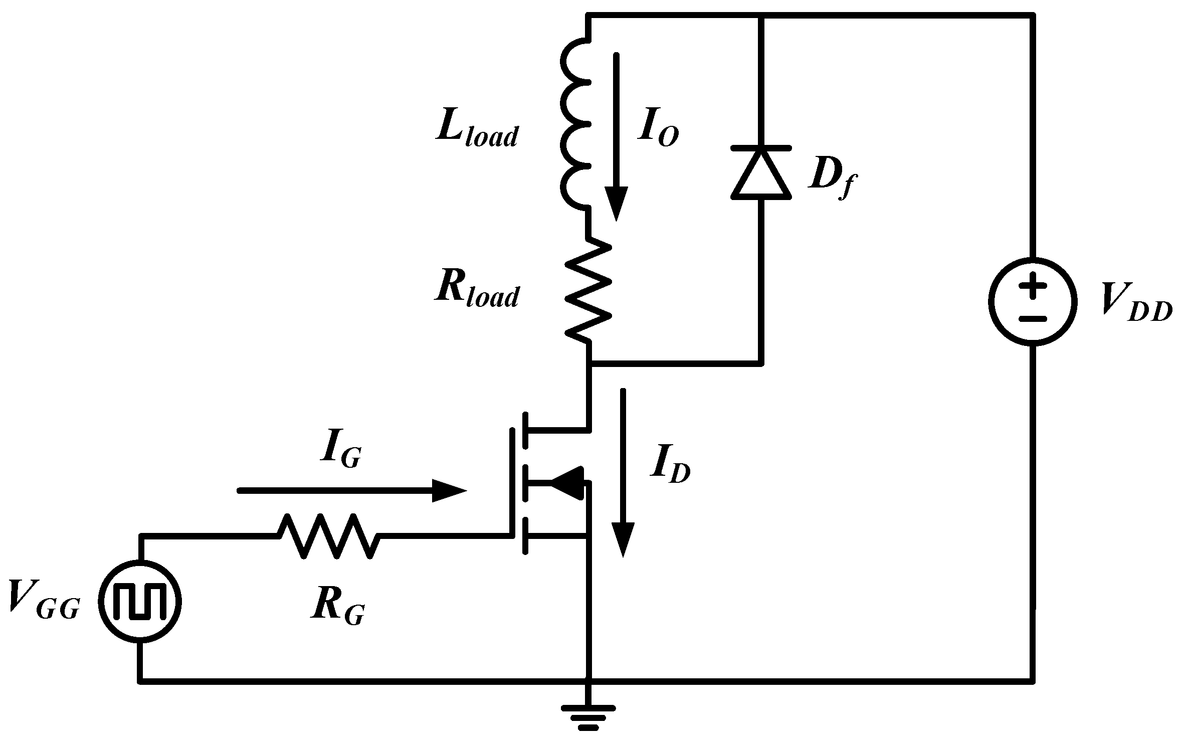
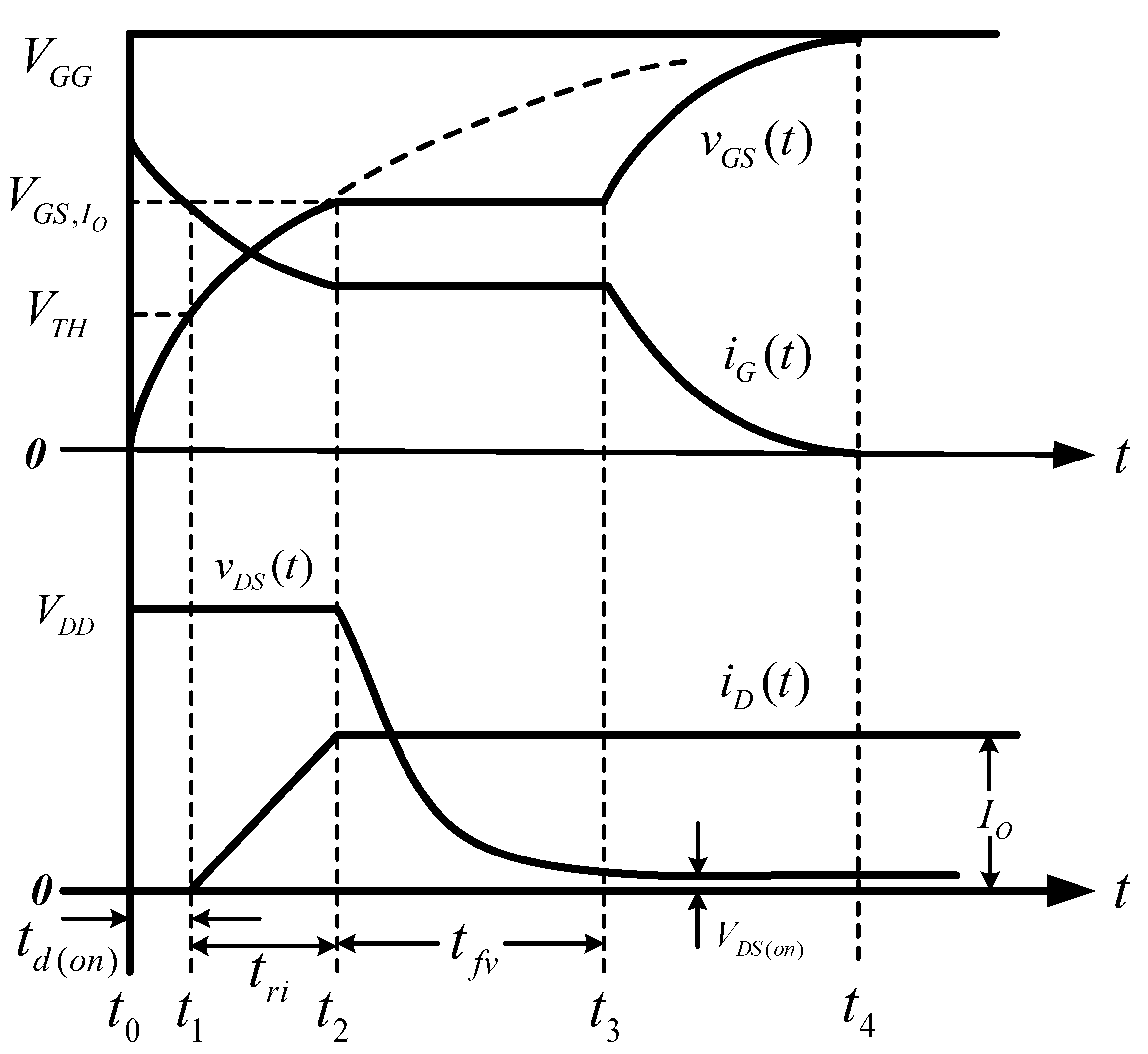
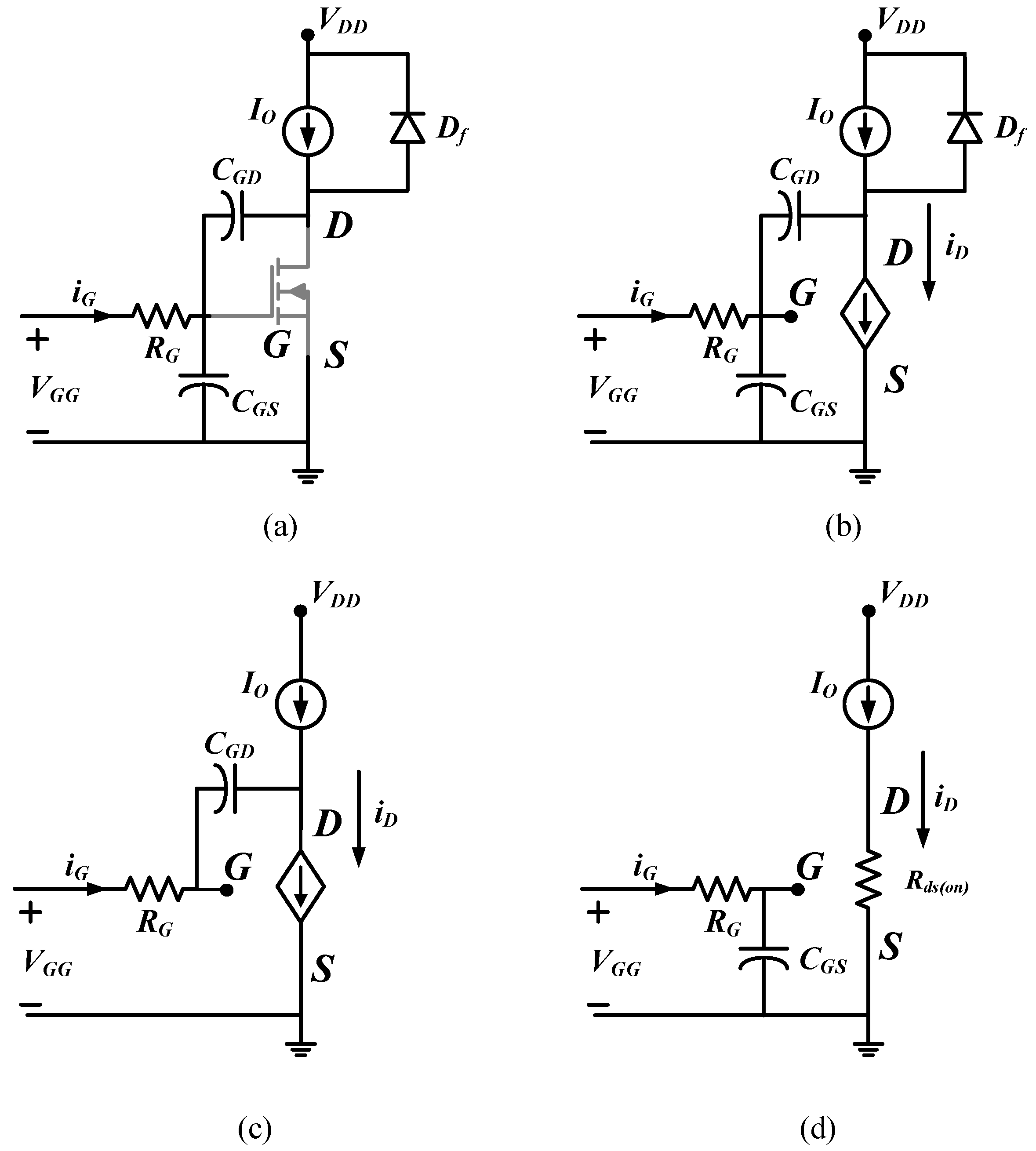
2.1. The Switching Characteristics of the SiC MOSFET

Dynamic voltage equalization is affected by the switching characteristics of SiC MOSFETs; the switching process is quantitatively analyzed based on the inductive clamp circuit [26]. The topology is shown in Figure 2. Since the turn-on and turn-off processes of SiC MOSFETs are similar, only the turn-on process is analyzed in this paper.
The relative schematic waveforms and the equivalent circuit diagram of the turn-on process are shown in Figure 3 and Figure 4, respectively. When the MOSFET is off, its gate–source voltage v G S and drain current i D are zero, and its drain–source voltage v D S is the bus voltage V D D . The clamp diode D f turns on and flows the load current I O . At t 0 , the gate–source voltage v G S rises.
[ t 0 t 1 ]: v G S rises from zero, the gate current i G charges the input capacitor. Since gate–source capacitance C G S is much larger than gate–drain capacitance C G D , most of the gate current i G charges C G S and a small amount flows to C G D . Since v G S is below the MOSFET threshold voltage V T H , i D remains at zero, and v D S remains constant. The time required for v G S to rise from zero to the threshold voltage V T H is called the turn-on delay time t d ( o n ) , which is derived as follows:
i G ( t ) = V G G v G S ( t ) R G = C G S d v G S ( t ) d t C G D d ( v G S ( t ) v D S ( t ) ) d t
v D S is constant and equal to the bus voltage V D D in this interval; the expression for i G is shown in (2):
i G ( t ) = ( C G S + C G D ) d v G S ( t ) d t
Based on (1) and (2), and the initial condition v G S ( t 0 ) = 0, v G S can be expressed by (3) and (4) in this interval:
v G S ( t ) = V G G ( 1 e ( t t 0 ) ( t t 0 ) τ τ )
τ = R G ( C G S + C G D )
where R G is the gate resistance of the MOSFE; i G can be expressed as (5)
i G = V G G R G e ( t t 0 ) ( t t 0 ) τ τ
[ t 1 t 2 ]: This interval is also known as the current rise interval. After t 1 , v G S > V T H , i G continues to charge the input capacitance C i s s , and v G S continues rising. i D rises as a function of v G S from the t 1 moment and the MOSFET enters the saturation operating region.
The transconductance g m and i D are given by (6) and (7), respectively:
g m = i D v g s = 2 I D S S i D V T H
i D ( t ) = g m ( v G S V T H )
where I D S S is the MOSFET drain current at zero gate bias.
Since i D < I O in this interval, D f is still conducting the load current and v D S = V D D . The expression for v G S agrees with Expression (3). Expression (3) is associated with (7) to obtain Expression (8) for i G , which can be seen to decrease exponentially in i G :
i G ( t ) = g m ( V G G V T H ) g m V G G e ( t t 1 ) ( t t 1 ) τ τ
At t 2 , i D reaches the load current I O and D f turns off. The current rise phase time interval t r i satisfies (9):
t r i = τ ln g m V G G g m ( V G G V T H ) I O
[ t 2 t 3 ]: This interval is also known as the Miller plateau interval. At t 2 , i D reaches the load current and remains constant. The MOSFET operates in the saturation region and v G S remains constant. The Miller platform voltage V G S , I O is expressed as (10)
V G S , I O = I O g m + V T H
i G ( t 2 ) can be expressed as (11):
i G ( t 2 ) = V G G v G S ( t 2 ) R G = V G G ( I O I O g m g m ) V T H R G
In this interval, v G S is constant and i G begins to charge C G D . The Formula (12) for i G can be obtained as follows:
i G ( t ) = C G D d ( v G v D ) d t
Since V G S remains constant, Expression (13) can be obtained:
i G ( t ) = C G D d v D S d t = V G G V G G , I O R G = V G G V T H I O I O g m g m R G
The initial condition is v D S ( t 2 ) = V D D at t 2 , and bringing in (13) yields an expression for v D S over time within the interval:
v D S ( t ) = V G G V G S , I O R G C G D ( t t 2 ) + V D D
As the gate drive current charges C G D , v D S decreases linearly. At this point, the MOSFET gradually enters the linear operating region. The larger V D D is, the longer the Miller platform phase lasts. At t 3 , v D S drops to the on-state drain–source voltage drop V D S ( o n ) , where V D S ( o n ) = I D R d s ( o n ) . The Miller platform duration t f v is given by (15):
t f v = t 3 t 2 = R G C G D ( V D D I D R d s ( o n ) ) V G G V T H I O I O g m g m
[ t 3 t 4 ]: After t 3 , v G S continues to rise under the continued charging of i G . Since v D S remains constant at this point, the rate of rise of v G S can be referred to the phase [ t 0 t 1 ].
v G S ( t ) = V G G ( 1 e ( t t 3 ) ( t t 3 ) τ τ )
During this interval, v G S grows exponentially until the driving voltage V G G is reached. At t 4 , i D becomes zero and the MOSFET turn-on process ends. The total turn-on delay t O N is the summation of the three part-time intervals and is given by (17):
t O N = t d ( o n ) + t r i + t f v

2.2. The Dynamic Voltage Distribution Analysis of the Series-Connected SiC MOSFETs

Ideally, series-connected SiC MOSFETs would achieve good dynamic and static voltage equalization. However, in actual circuits, due to the impossibility of achieving perfectly uniform devices and highly symmetrical driving circuits, the voltage equalization effect often differs from the ideal situation. The device and circuit factors affecting the dynamic voltage equalization characteristics of series-connected SiC MOSFETs are theoretically investigated in what follows.
Figure 5 shows the equivalent switching model for SiC MOSFETs, where C G D and C D S are related to the drain–source voltage V D S , while C G S can be considered to be constant. The input capacitance C i s s of the MOSFET consists of capacitance C G D and C G S . The output capacitance C o s s includes capacitance C D S and C G D . Furthermore, the feedback capacitance C r s s is the capacitance C G D . The model includes gate parasitic inductance L G and source-level parasitic inductance L S . Parasitic inductance is introduced by the interconnections and affects the switching process of the devices.
The dynamic voltage inhomogeneity of series SiC MOSFETs is mainly caused by two aspects, gate drive circuit delay differences and device parameter differences. Furthermore, differences in parasitic parameters on the main circuit may cause voltage unevenness. Among them, series SiC MOSFET static voltage equalization is mainly affected by the device turn-off leakage current. The device dynamic voltage equalization is affected by more factors, including device dynamic characteristic differences, gate drive delay mismatch, and different parasitic parameters on the main circuit. Device dynamic characteristics such as threshold voltage V T H , inter-pole parasitic capacitance, transconductance g m , parasitic inductance, etc., all affect the dynamic voltage equalization of series-connected SiC MOSFETs. The causes of voltage imbalance during turn-on and turn-off will be analyzed separately in the following section.
Based on the quantitative description of the SiC MOSFET switching process, it can be assumed that the following factors may be responsible for the voltage imbalance of series-connected SiC MOSFETs during the turn-on phase:
(1)
The difference at the moment when the MOSFET enters the current rise phase ( t r i ). There are two sources of this difference, one is the gate drive delay difference, which is due to the gate drive circuit difference; the other is the difference in the turn-on delay time ( t d ( o n ) ) of individual MOSFETs, which is mainly due to the threshold voltage V T H and input capacitance C i s s differences. During the current rise interval, the MOSFET can be equated to a gate voltage-controlled current source. At this point, the MOSFET can be viewed as an ever-decreasing resistor from the drain–source point of view. If the MOSFET enters this stage later, its equivalent drain–source resistance is relatively large, and, thus, its drain–source voltage is large. The difference in the stage of current rise entered by each MOSFET can lead to uneven voltage.
(2)
MOSFETs have different rates of current change during the current rise interval ( t r i ). According to (8), the difference in transconductance of each MOSFET will result in a different rate of current rise. This is due to unavoidable differences in device fabrication. From the drain–source point of view, the equivalent resistance of each MOSFET will be different. Uneven voltage may occur at this stage.
(3)
MOSFETs have different rates of voltage change during the voltage drop interval ( t f v ). In this interval, MOSFET can be equivalent to a variable capacitor, and its capacitance rises as the drain–source voltage falls. Thus, the difference in output equivalent capacitance can lead to uneven voltage. However, since the total voltage to which the series MOSFETs are subjected at this stage has already begun to fall, voltage unevenness does not normally lead to serious problems.
In general, the main reasons for the uneven voltage of series-connected SiC MOSFETs in the turning-off process are as follows:
(1)
The difference at the moment when the MOSFET enters the voltage rise phase ( t r v ). There are two sources of this difference, one is the gate drive delay difference, which is due to the gate drive circuit difference; the second is the difference in the turn-off delay time ( t d ( o f f ) ) of each MOSFET, which is mainly due to the difference in the threshold voltage V T H and the input capacitance C i s s . In this interval, the MOSFET can be equated to a variable capacitor and its capacitance decreases as the drain–source voltage rises. The voltage rise interval can be considered as a charging process of the ever-smaller MOSFET output capacitance. MOSFETs that turn off early are necessarily subjected to higher drain–source voltages. If the difference in MOSFET turn-off delay is too large, it is easy to cause overvoltage damage to the MOSFET. According to theoretical analyses and experimental results, the turn-off delay difference [27] is considered to be the main factor affecting the turn-off voltage equalization of series-connected SiC MOSFETs. Thus, it is quite important to ensure that the series SiC MOSFET turn-off delay is synchronized.
(2)
The difference in the rate of voltage change of MOSFETs during the voltage rise phase ( t r v ). Even though the drain–source voltage of each MOSFET in the series starts to rise at the same time, the difference in the rate of voltage change of the MOSFETs at this stage is difficult to avoid. The MOSFET at this stage can be equated to the charging process of a variable capacitor. The rate of voltage change during the Miller plateau period d V d V d t d t is mainly determined by the gate drive current and the MOSFET feedback capacitance C r s s . Due to device fabrication differences, the feedback capacitance is different, causing the MOSFET voltage imbalance at this stage.
(3)
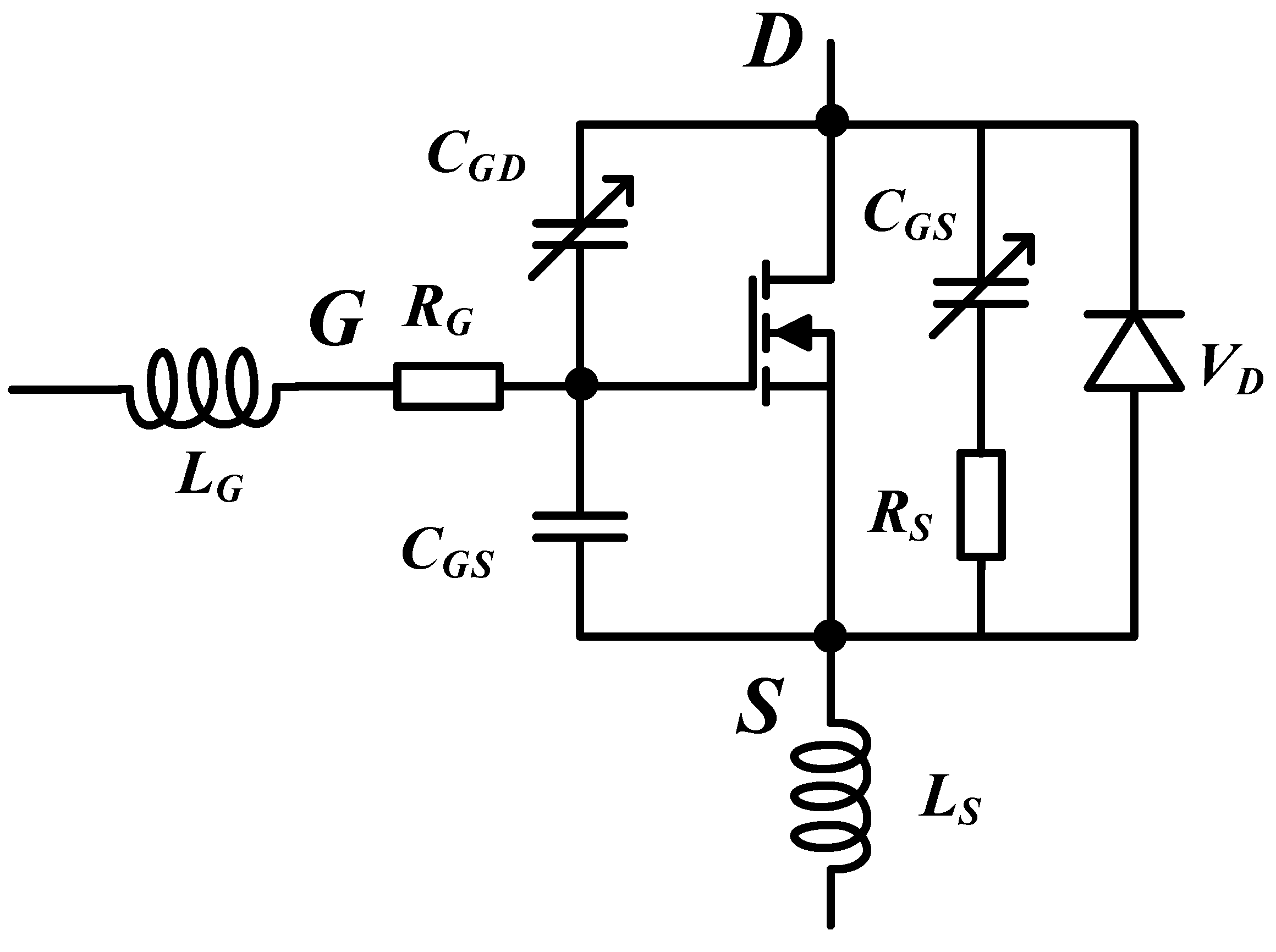
Circuit stray capacitance. Relevant studies have shown that [28] even if the driver circuit and the MOSFET are kept the same, the difference in stray parasitic capacitance will still cause uneven turn-off voltage. There are two main sources of stray capacitance. The first is the unavoidable stray capacitance that exists between the gate driver and ground, mainly the transformer coupling capacitance. The second is the parasitic stray capacitance between each port of the MOSFET on the main circuit and ground, which is related to device placement and PCB layout.
(4)
MOSFETs have different rates of current change during the current drop phase ( t f i ). At this point in this interval, the MOSFET can be regarded as an ever-increasing resistance from the drain–source point of view. The unavoidable difference in transconductance between the MOSFETs will result in a difference in the equivalent resistance of each MOSFET, which leads to an imbalance in the MOSFET drain–source voltage.

2.3. The Simulation of the Dynamic Voltage Distribution

Since the voltage imbalance in the turn-off transient is more critical than the voltage imbalance in the turn-on transient, in this section, the factors affecting the voltage equalization during turn-off was verified by PSpice simulation.
The simulation circuit is shown in Figure 6a. The bus voltage V D C was set to 2000 V, and the MOSFET gate resistors were all set to 20 Ω. The MOSFETs were driven by a pulse signal source V p u l s e , and their turn-on and turn-off voltages were +20 V and −2 V, respectively. SCT20280KE is a typical SiC MOSFET co-packaged with SiC-SBD. The co-packaged SiC SBD can protect the MOSFET from being broken down, which is suitable for serially connected applications. The SiC MOSFET applied in the simulation was Rohm’s SCT2080KE. Table 1 lists the related parameters of the simulation model.
The V D S voltage unbalanced waveform during turn-off in the theoretical analysis is shown in Figure 6b. To characterize the degree of series SiC MOSFET V D S imbalance at turn-off, the turn-off voltage imbalance factor α o f f is introduced in this paper. For a two-tube series SiC MOSFET, the voltage imbalance coefficient α o f f at turn-off is defined as shown in (18):
α o f f = Δ V d V d V d 2 2 × 100 %

The Driver Delay Variance Affection

To verify the effect of the drive delay difference t o f f on the turn-off voltage distribution of series-connected SiC MOSFETs, the delay of the gate drive signal V p u l s e of a single MOSFET is adjusted to obtain the voltage distribution difference while keeping other parameters constant. Figure 7 shows the voltage imbalance coefficient α o f f versus the delay difference t o f f .
As shown in Figure 7, α o f f has an approximately linear relationship with t o f f . According to the previous analysis, the difference in gate signal delay will lead to the difference when the MOSFET enters the voltage rise phase ( t r v ). According to the MOSFET switching characteristics, it can be assumed that the gate signal delay difference does not affect the MOSFET drain–source voltage rise rate. The voltage distribution and α o f f can be obtained if the two MOSFET voltage rise rates are the same.
Δ V d = t o f f 2 d V D S d t
α o f f = t o f f V d d V D S d t
The MOSFET voltage rise rate was calculated to be 19.3 kV/μs. Due to the fast switching speed of SiC MOSFET, the voltage rise rate was high. Therefore, gate delay drive differences can lead to severe turn-off voltage inhomogeneity.

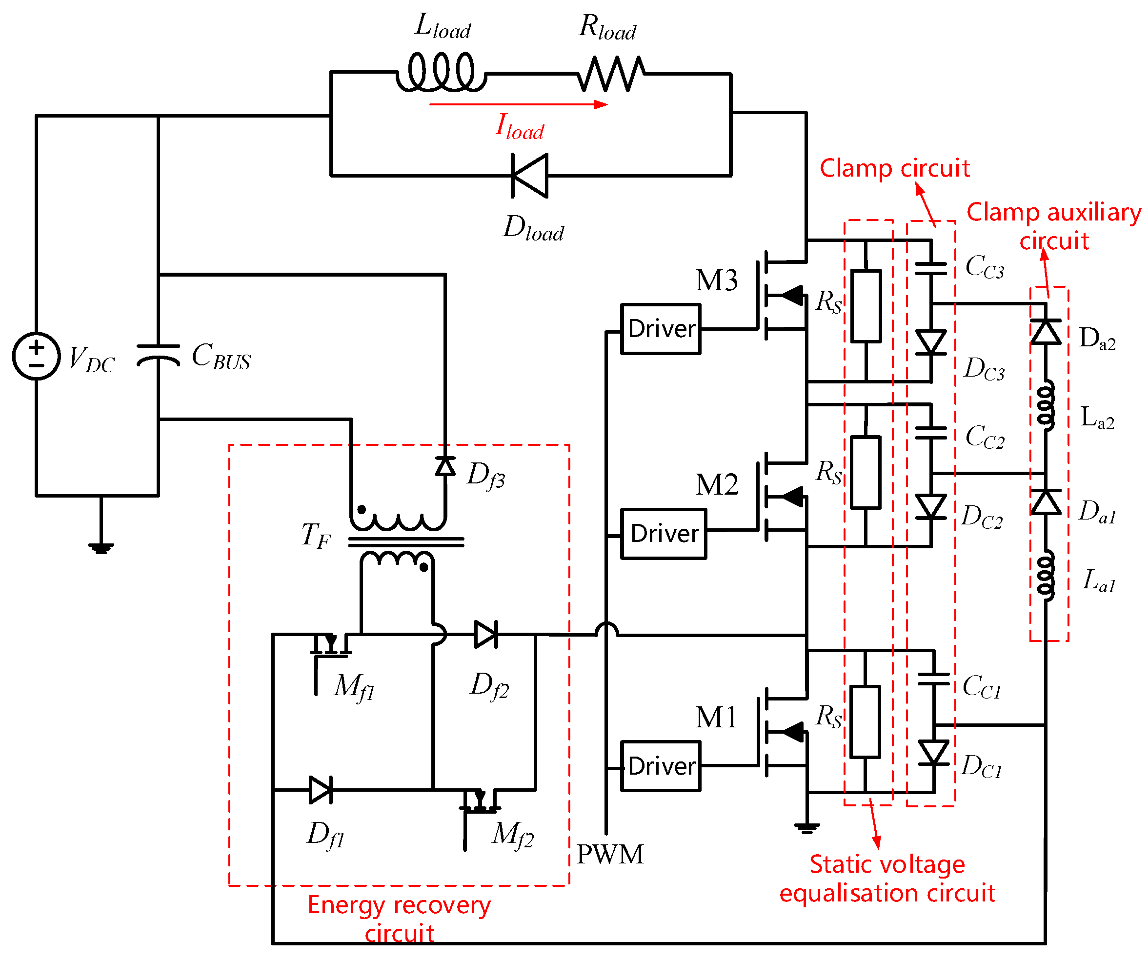
3. The Novel Series SiC MOSFET Topology Design

The new series SiC MOSFET topology consisted of a series SiC MOSFET, a clamp circuit and its clamp auxiliary circuit, and an energy recovery circuit, which can be used as a power switch in power electronics. The topology is shown in Figure 8. In this section, the inductive clamp circuit was used as the main power circuit to illustrate the working principle and parameter selection principle of the series SiC MOSFET topology, where V D C is the input bus voltage, and C B U S is the bus capacitance.
The topology consists of series SiC MOSFETs M1, M2, and M3. PWM is the main switching tube control signal. The circuit load is an inductor L l o a d and a resistor R l o a d , and D l o a d is a continuity diode. D l o a d is the continuity diode, and R S is the static voltage equalizing resistor. A clamp circuit is connected in parallel with the drain–source of each MOSFET, consisting of clamp diode D C and clamp capacitor C C . The current-limiting inductor L a and the auxiliary diode D a form the clamping auxiliary circuit. The two-tube flyback DC/DC circuit serves as an energy recovery circuit, and its input and output are clamp capacitor C C 1 and bus capacitor C B U S , respectively. M f 1 and M f 2 are the switching tubes of the two-tube flyback circuit. Diodes D f 1 and D f 2 protect the switching tubes. The T F is a flyback transformer for voltage isolation and energy transfer.
As the designer was familiar with the clamp circuit and clamp auxiliary loop, this paper only focuses on the energy recovery circuit. The energy recovery circuit has two effects; the first one is to limit the clamp capacitance voltage, and the second one is to transfer the energy accumulated in the clamped capacitor back to the bus capacitor for reuse to reduce losses. The feedback control circuit will determine whether to turn on the energy recovery circuit switching tube based on the sampled capacitor C C 1 voltage. The energy recovery circuit only works when the capacitor C C 1 ’s voltage exceeds the rated value.

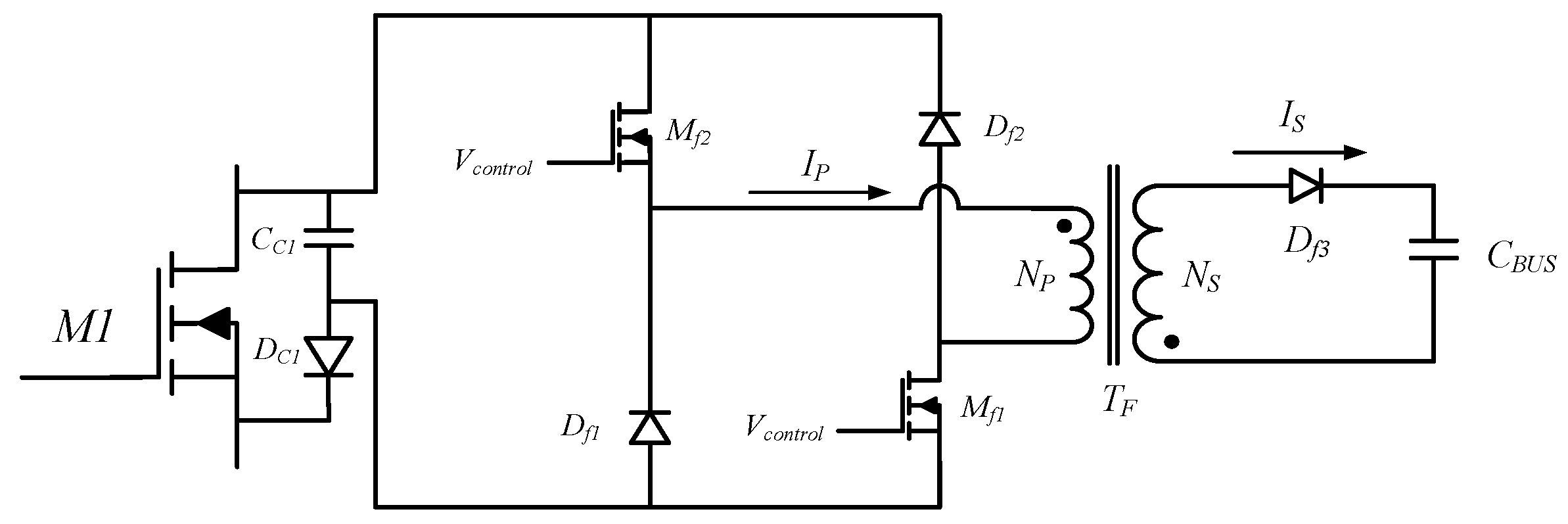
3.1. The Energy Recovery Circuit Design

The energy recovery circuit is based on a double-tube flyback DC/DC circuit, as shown in Figure 9. Compared with the single-tube flyback circuit, the double-tube flyback circuit reduces the MOSFET withstand voltage requirement and effectively avoids the voltage spike caused by the transformer leakage inductance during turn-off. The flyback transformer T F plays the role of electrical isolation and energy transfer, and its turns ratio is given by N = N P / N S . The switching of the switching tubes M f 1 and M f 2 is controlled by the output signal V c o n t r o l from the feedback control circuit. Since the energy recovery circuit operates in PFM mode with variable switching frequency, the two-tube flyback circuit designed in this paper operates in DCM mode. Compared with the CCM mode, the flyback circuit in the DCM mode is simple to calculate, easy to realize, and less prone to magnetic saturation.
The working waveform of the energy recovery circuit is shown in Figure 10, and its working process circuit diagram is shown in Figure 11. Its working process is divided into two stages, the primary coil energy storage stage and the secondary coil discharge stage:
(1) Primary coil energy storage stage: this stage of the circuit is shown in Figure 11a. C C 1 voltage is too high before t 0 and the feedback control circuit output V c o n t r o l becomes high at t 0 . At this time, V C 1 = V 0 , and the primary coil current i P = 0. The switching MOSFET M f 1 and M f 2 are turned on, and the primary coil N P stores energy, and i P continues to rise. C C 1 releases energy and V C 1 decreases from V 0 . The pulse signal V c o n t r o l lasts for t p u l s e . During the phase [ t 0 t 1 ], the inductance L P of the primary coil of the flyback transformer resonates with the capacitance C C 1 and i P can be assumed to rise linearly during this period:
i P ( t ) = V 0 L P ( t t 0 )
At this stage, the secondary coil current i S = 0. D f 3 is off and it is subjected to a reverse voltage V d :
V d = V C 1 N + V D C
(2) Secondary coil discharge stage: this stage of the circuit is shown in Figure 11b. At t 1 , V c o n t r o l becomes low and i P reaches its maximum value I P m a x . M f 1 and M f 2 are switched off and the primary coil N P releases energy to the secondary coil N S .
I P max = t p u l s e V 0 L P
During the phase [ t 0 t 1 ], V C 1 continues to fall, and, at the moment t 1 , V C 1 falls to V 1 .
V 1 = V 0 ( 1 t p u l s e 2 2 L P C C 1 )
The secondary coil N S back-excites the current at t 1 , when i S reaches its maximum value I S m a x = N · I P m a x , as shown in Figure 11b. In the [ t 1 t 2 ] stage, D f 3 conducts, the secondary coil N S releases energy to the bus capacitance C B U S , and the i S decreases linearly:
i s S ( t ) = t p u l s e V 0 · N L P V D C L P ( t t 1 )
where L S is the transformer secondary coil inductance. The [ t 1 t 2 ] phase duration t S is
t S = I S max · L S V D C = t p u l s e V 0 V D C · N
During the [ t 1 t 2 ] stage, there is a reflected voltage V N P on the primary coil of the transformer, which satisfies (27). Due to the presence of transformer leakage inductance, relatively large voltage spikes will be generated when M f 1 and M f 2 are switched off at t 1 . The leakage inductance energy of the primary coil N P can be returned to the capacitor C C 1 through D f 1 and D f 2 to avoid voltage spikes to protect the switching tube.
V N P = N ( V D C + V D )
I S drops to zero at t 2 , D f 3 will turn off, and the circuit operates in DCM mode. To ensure that the flyback circuit operates in intermittent mode, (28) needs to be satisfied:
t S + t p u l s e = t p u l s e ( 1 + V 0 V D C · N ) < 1 f max
Without considering losses, if the flyback circuit operates at a frequency of f m a x , the power delivered is P S , which is also the energy released by C C 1 . The increase in C C 1 energy due to the action of the clamp circuit and the clamp auxiliary circuit will be passed back to the bus capacitor through the flyback circuit, ensuring that V C 1 does not become too high.
P S = 1 2 t p u l s e 2 · V 0 2 · f m a x L P

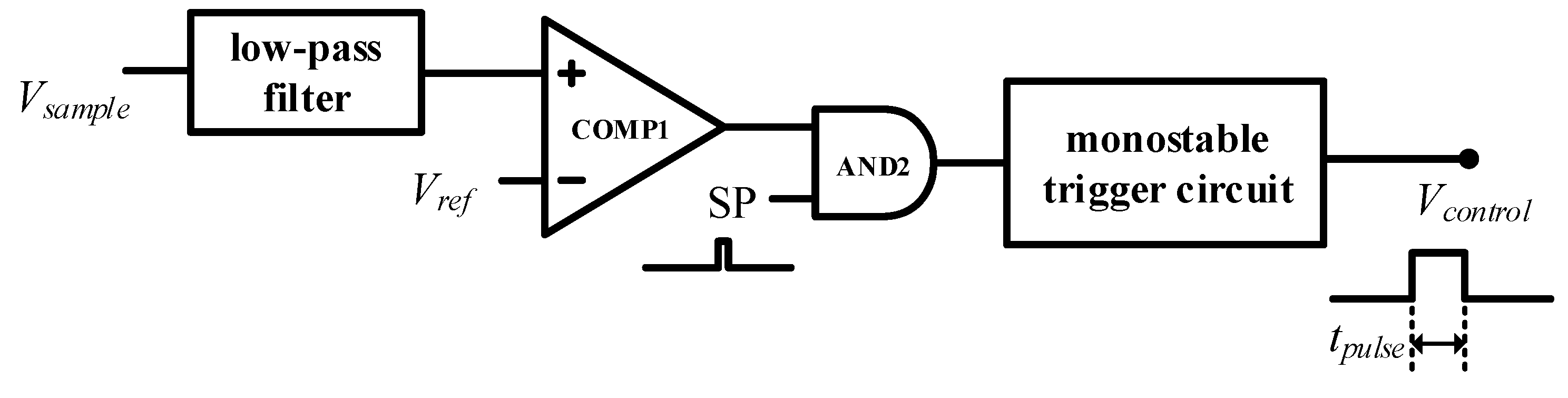
3.2. The Feedback Control Circuit Analysis
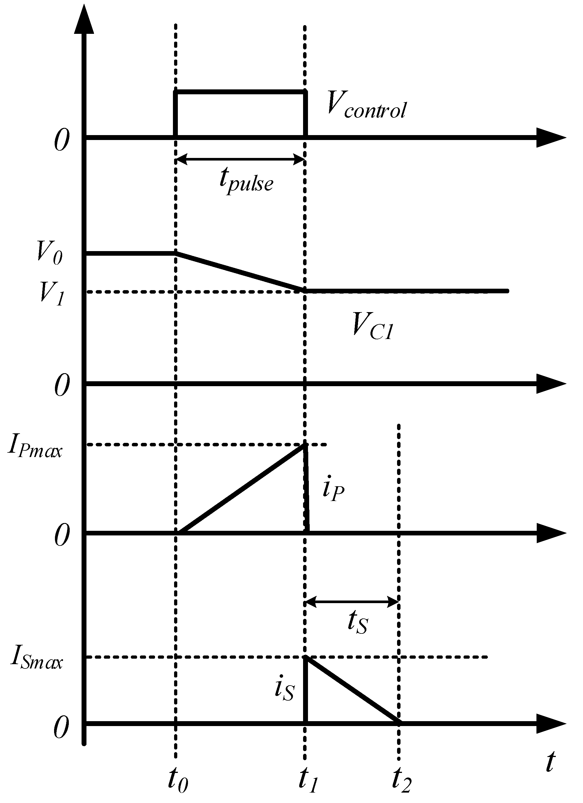
The feedback control circuit of the energy recovery circuit designed in this paper is shown in Figure 12, where V s a m p l e is the voltage V C 1 of the clamp capacitor C C 1 sampled by the Hall voltage sensor. To suppress the noise interference of the power circuit on the sampled output signal, V s a m p l e is followed by an active low-pass filter to filter out the high-frequency noise. The monostable trigger circuit will be triggered at the rising edge of the input signal and output a control signal V c o n t r o l with a certain pulse width. The V c o n t r o l is the input signal of the energy recovery circuit driver circuit, which is used to control the energy recovery circuit switching tube. The maximum voltage allowed by the clamping capacitor is V C 1 m a x ; when V C 1 exceeds V C 1 m a x , the sampled signal V s a m p l e will be larger than the reference signal V r e f . At this time, COMP1’s output is high, indicating that the capacitor C C 1 ’s voltage is too high.
The SP signal is a high-level pulse width small period square wave that determines whether the comparator COMP1’s output is valid or not. When the short pulse signal SP goes high, there are two cases for the comparator COMP1’s output. If COMP1’s output is low, it indicates that V C 1 is lower than the allowed maximum voltage V C 1 m a x , and the output of AND2 is low. The monostable trigger circuit output is low. If COMP1’s output is high, it indicates that V C 1 is higher than the allowed maximum voltage V C 1 m a x . The output of AND2 changes from low to high and triggers the monostable trigger circuit. The monostable trigger circuit will output a high-level pulse to control the energy recovery circuit. As the comparator COMP1’s output is only effective when the short pulse signal SP is high, this can effectively reduce the false trigger caused by sampling error or comparator output noise. The frequency of the SP signal is the maximum operating frequency of the energy recovery circuit. The relative waveforms are shown in Figure 13.
(1)
Before t 0 , since V C 1 is high enough, the V s a m p l e will be higher than V r e f , and then, COMP1’s output is high. However, SP is low and AND2’s output is still low.
(2)
At t 0 , SP becomes high and lasts for a short time. Since the COMP1 output is high, the AND2 output changes from low to high. This rising edge will trigger a monostable trigger to generate a V c o n t r o l signal with a pulse width of t p u l s e for controlling the energy recovery circuit. The operation of the energy recovery circuit is shown in Figure 10. During phase [ t 0 t 2 ], the switching tube of the energy recovery circuit is switched on. During this phase, the V C 1 continues to drop and energy is transferred to the primary coil of the flyback transformer.
(3)
At t 2 , V c o n t r o l becomes low. The switching tube of the energy recovery circuit turns off, and the transformer’s secondary coil back-excites the current. Although V C 1 has dropped to the permissible value, the comparator COMP1’s output is still high. This is due to the delay of the Hall voltage sensor, which does not reduce the COMP1 output until the moment t 3 after the t S D time. During the [ t 2 t 4 ] phase, V C 1 may rise due to the activation of the clamp capacitor and the clamp auxiliary circuit.
(4)
At t 4 , the SP signal becomes high and the period of the SP signal is t S P . If V C 1 ’s voltage rises more in the phase [ t 2 t 4 ], causing the COMP1 output to be high at t 4 , the monostable flip-flop will be activated next, repeating the process (1)–(3). If V C 1 is small and does not exceed the predetermined voltage in the phase [ t 2 t 4 ], the COMP1 output is low at t 4 , the AND2 output is low and the monostable flip-flop will not operate. The monostable circuit operation will be decided Until the next rising edge of the SP signal according to the COMP1 output.
If the switching process of the series-connected MOSFETs and the driver circuit varies greatly, it will result in a large ripple voltage of each clamp capacitor during the switching process. In this case, V C 1 will rise rapidly. To limit the rise of V C 1 , the energy recovery circuit switching frequency must be larger; in contrast, if the series-connected MOSFETs and drive circuits are highly consistent, the switching process of each clamp capacitor ripple voltage is smaller. In this situation, V C 1 rises slowly, and the energy recovery circuit switching frequency is small. Ideally, if each MOSFET switching process is identical, V C 1 will not rise. At this time, the energy recovery circuit operating frequency is zero. In summary, the operating frequency of the energy recovery circuit depends on the degree of difference in the switching process of each MOSFET in the series-connected MOSFET.
Based on the above analysis, it can be seen that, if COMP1’s output signal is high every time the SP signal is high, the monostable flip-flop will continuously output pulses, which occurs when the difference in the switching process of each MOSFET is too large. Therefore, the maximum frequency of the flyback circuit operation is equal to the frequency of the SP signal f m a x = 1/ t S P . According to (29), the maximum power delivered by the flyback circuit is P S m a x .
P S max = 1 2 t p u l s e 2 · V 0 2 · f max L P
The maximum power P S m a x in the worst case needs to be taken into account when the flyback circuit operates at the maximum frequency V C 1 . Consideration needs to be given to the value of the energy that will be accumulated by the clamp capacitor due to the clamping action when the difference in drive delay between the MOSFETs is at its maximum, and P S m a x needs to be ensured to be greater than the amount of energy that will be accumulated due to the clamping action. For the three-tube tandem SiC MOSFET topology in this paper, when only the turn-off process is considered, it is assumed that the M3 drive signal is delayed t D 1 to M1, while the M2 drive signal is delayed t D 2 to M1. Then, the maximum power P S m a x of the flyback circuit needs to satisfy (31):
t D 1 + t D 2 · I l o a d · V D C 3 · f P W M < P S max
If t D 1 and t D 2 are assumed to be 100 ns and 200 ns, respectively, it is a serious case for series-connected SiC MOSFETs. When the bus voltage is 2800 V and the load current is 10 A, the maximum power of the flyback circuit needs to be higher than 140 W. With the turn-on phase considered, the maximum power of the flyback circuit should be greater than the calculated value in (31), which can be taken to be about 1.5–2 times the calculated value. For series n-MOSFETs, the maximum capacitance of V C 1 m a x needs to be set to be slightly larger than the equilibrium voltage V D C /n, and, at the same time, V C 1 m a x needs to be smaller than the breakdown voltage of the MOSFET. In this paper, V C 1 m a x is larger than V D C /n by 30–50 V. If V c o n t r o l pulse width is set to 10 μs, and the inductance of the primary coil of the flyback transformer is set to 1.5 mH, the maximum current of the primary coil is 6.5 A. The maximum power of the designed flyback transformer is 210 W, and it can meet the design requirements. Flyback circuit design needs to consider the switching device voltage stress. This paper takes the margin of switching device voltage stress as 20%. According to (22), the diode D f 3 is subjected to the maximum reverse voltage at t 0 . Its rated reverse voltage V F needs to satisfy the relation (32):
0.8 V F > V 0 N + V D C
According to (27), M f 1 and M f 2 are subjected to the maximum reverse voltage at t 1 . The rated voltage V M O S of M f 1 and M f 2 needs to satisfy the relation (33):
2 × 0.8 V M O S > N ( V D C + V D ) + V 1
In this paper, we took N = 0.316, and set V 0 = 930 V and V 1 = 950 V. According to (22), the diode reverse voltage V F is >7200 V, which was realized by connecting six 1200 V SiC SBDs in series. According to (27), V M O S > 1146 V, which was realised by using 1200 V SiC MOSFETs.

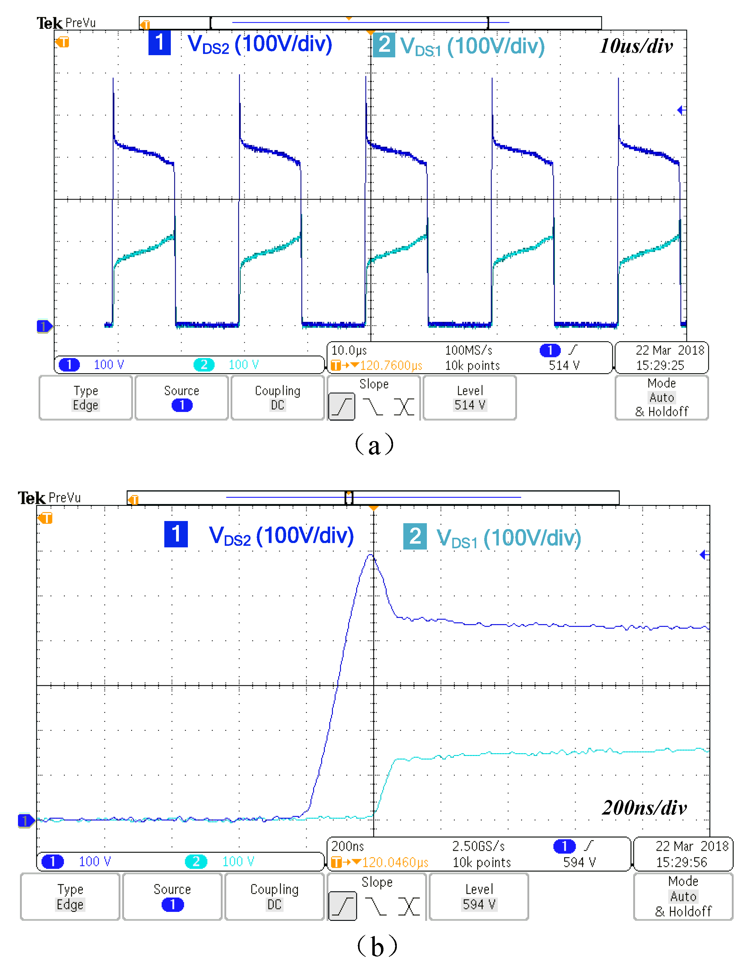
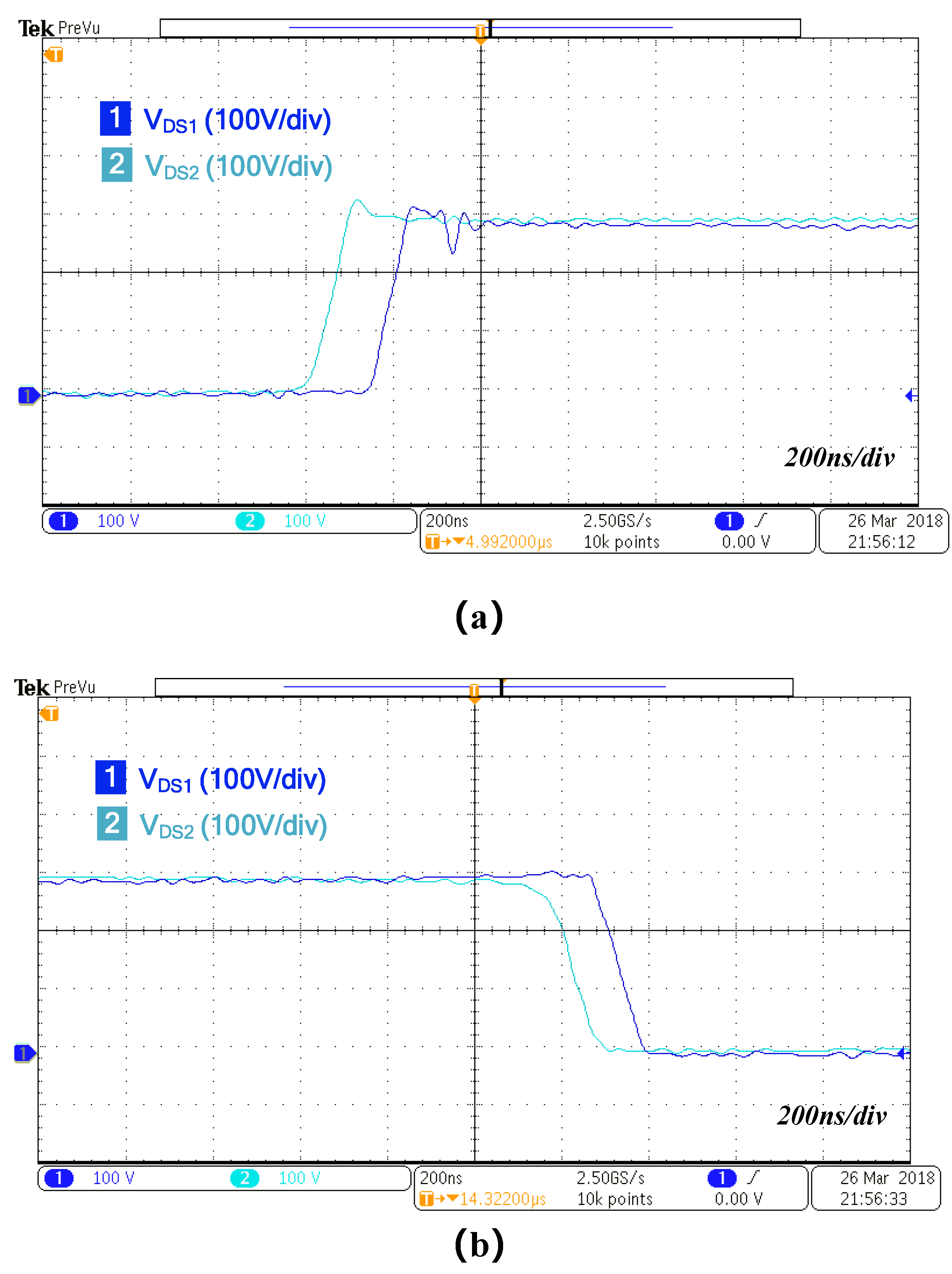
4. The Experimental Results

A prototype was also fabricated and tested to verify its effectiveness. The overall circuit of the test is shown in Figure 14, where M1 and M2 are two SiC MOSFETs connected in series. The prototype is shown in Figure 15. The main parameters of the converter are in Table 2, and the parameters of the SiC MOSFET are listed in Table 3.
In this paper, the input voltage of the main Buck circuit was set to 600 V, and the duty cycle of the Buck circuit was set to 50%, which was used to complete the 300–600 V Buck conversion. The average current of the main inductor L l o a d was 10 A; then, the power of the main circuit design was 2.8 kW.
To verify the effectiveness of the strategy, the gate resistors of M1 and M2 were set differently; the M1 gate resistance was set to be 33 ω , while the M2 was 0 ω . M1 and M2 were directly connected in series without applying other circuits, and the drain–source voltages of the two MOSFETs, V D S 1 and V D S 2 , are shown in Figure 16.
Figure 16b shows the voltage distribution during turn-off. Due to the small M2 gate resistance, M2 turns off first and V D S 2 rises first during the turn-off interval. The delay difference between the two MOSFETs during turn-off is 200 ns. In this case, V D S 2 rises directly to the bus voltage of 600 V. M1 is then turned off, resulting in severe voltage unevenness during turn-off. The difference between the two V D S in the static state is slightly reduced due to the static voltage equalizing resistor. This experiment verifies that different driving delays will cause voltage unevenness, which seriously affects the safe operation of series-connected SiC MOSFETs.
The tested results in the same case with the proposed strategy are shown in Figure 17. The voltage distribution during turn-off is slightly different from cycle to cycle because the clamp capacitor voltage changes from cycle to cycle. During both turn-on and turn-off intervals, the maximum MOSFET voltage does not exceed 320 V. Comparing with Figure 16, it can be seen that this topology can effectively limit the drain–source voltage rise, and ensure that the dynamic and static voltages of series-connected SiC MOSFETs are balanced.
The variation curves of the two MOSFET V D S during switching are shown in Figure 18. Figure 18b shows the turn-off detail. It can be seen that M2 turns off first, causing V D S 2 to start rising. When V D S 2 rises to the clamp capacitor voltage, the clamp circuit turns on, and V D S 2 stops rising. Then, M1 turns on, and V D S 1 starts to rise. It can be seen that this topology can limit the MOSFET drain–source voltage from being too high during the shutdown.
Figure 18b shows the curve of V D S ’s change during the turn-on process. M2 turns off first, leading V D S 2 to start falling. There is no voltage spike in the turn-on process.
The experimental results are the same as the analysis above. The voltage spike in the turn-off interval is suppressed from 600 V to 320 V.

5. Conclusions

A comparison was made between state-of-the-art approaches and the approach proposed in this work; the results are shown in Table 4. Compared to other approaches, this work achieved energy recovery at the cost of six power devices. Due to the relative simplicity of the control method in this work, the number of analog devices used was low.
Based on the analysis above, when increasing the number of series-connected SiC MOSFETs, this method only requires adding simple auxiliary circuits to the device without changing the energy recovery circuitry, which has a small impact on the circuit complexity. The energy recovery circuit uses a transformer and is the largest part of the auxiliary circuit. Since the energy recovery circuit operates at a lower frequency and processes less energy per cycle, it has the possibility of magnetic integration with the magnetic devices of the main circuit under certain conditions.
Based on the analysis above, this strategy has some advantages. Firstly, the approach is effective; the voltage spike is suppressed from bus voltage 600 V to 320 V. Secondly, the strategy realizes energy recovery, which is beneficial for efficiency. Thirdly, the drive strategy is simple; fewer analog devices are used.

Author Contributions

Conceptualization, S.S. and J.L.; methodology, P.L.; validation, P.L., S.S. and J.L.; formal analysis, S.S.; investigation, J.L.; resources, Y.Z.; data curation, W.Y.; writing—original draft preparation, P.L.; writing—review and editing, Y.S.; visualization, S.S.; supervision, Y.Z.; project administration, Y.Z.; funding acquisition, Y.Z. All authors have read and agreed to the published version of the manuscript.

Funding

This research was funded by Key R&D Program of Shaanxi Province grant number 2023-YBGY-005.

Data Availability Statement

Data are contained within the article.

Conflicts of Interest

The authors declare no conflicts of interest.

References

  1. Millán, J.; Godignon, P.; Perpiñà, X.; Pérez-Tomás, A.; Rebollo, J. A Survey of Wide Bandgap Power Semiconductor Devices. IEEE Trans. Power Electron. 2014, 29, 2155–2163. [Google Scholar] [CrossRef]
  2. Palmour, J.W. Silicon carbide power device development for industrial markets. In Proceedings of the 2014 IEEE International Electron Devices Meeting, San Francisco, CA, USA, 15–17 December 2014; pp. 1.1.1–1.1.8. [Google Scholar] [CrossRef]
  3. Song, Q.; Yang, S.; Tang, G.; Han, C.; Zhang, Y.; Tang, X.; Zhang, Y.; Zhang, Y. 4H-SiC Trench MOSFET With L-Shaped Gate. IEEE Electron Device Lett. 2016, 37, 463–466. [Google Scholar] [CrossRef]
  4. She, X.; Huang, A.Q.; Lucía, O.; Ozpineci, B. Review of Silicon Carbide Power Devices and Their Applications. IEEE Trans. Ind. Electron. 2017, 64, 8193–8205. [Google Scholar] [CrossRef]
  5. Song, Q.; Yuan, H.; Sun, Q.; Han, C.; Tang, X.; Zhang, Y.; Yuan, L.; Yang, S.; Zhang, Y. Reverse-Bias Stress-Induced Electrical Parameters Instability in 4H-SiC JBS Diodes Terminated Nonequidistance FLRs. IEEE Trans. Electron Devices 2019, 66, 3935–3939. [Google Scholar] [CrossRef]
  6. Yu, L.; Sheng, K. Modeling and Optimal Device Design for 4H-SiC Super-Junction Devices. IEEE Trans. Electron Devices 2008, 55, 1961–1969. [Google Scholar] [CrossRef]
  7. Bolotnikov, A.; Losee, P.; Permuy, A.; Dunne, G.; Kennerly, S.; Rowden, B.; Nasadoski, J.; Harfman-Todorovic, M.; Raju, R.; Tao, F.; et al. Overview of 1.2–2.2 kV SiC MOSFETs targeted for industrial power conversion applications. In Proceedings of the 2015 IEEE Applied Power Electronics Conference and Exposition (APEC), Charlotte, NC, USA, 15–19 March 2015; pp. 2445–2452. [Google Scholar] [CrossRef]
  8. Ferraro, A. An overview of low-loss snubber technology for transistor converters. In Proceedings of the 1982 IEEE Power Electronics Specialists conference, Cambridge, MA, USA, 14–17 June 1982; pp. 466–477. [Google Scholar] [CrossRef]
  9. Vechalapu, K.; Negi, A.; Bhattacharya, S. Comparative performance evaluation of series connected 15 kV SiC IGBT devices and 15 kV SiC MOSFET devices for MV power conversion systems. In Proceedings of the Energy Conversion Congress and Exposition (ECCE), Milwaukee, WI, USA, 18–22 September 2016; pp. 1–8. [Google Scholar]
  10. Busatto, G.; Cascone, B.; Fratelli, L.; Luciano, A. Series connection of IGBTs in hard-switching applications. In Proceedings of the Industry Applications Conference, 1998. Thirty-Third IAS Annual Meeting, St. Louis, MO, USA, 12–15 October 1998; Volume 2, pp. 825–830. [Google Scholar]
  11. Robinson, F.V.; Hamidi, V. Series connecting devices for high-voltage power conversion. In Proceedings of the 2007 42nd International Universities Power Engineering Conference, Brighton, UK, 4–6 September 2007; pp. 1134–1139. [Google Scholar] [CrossRef]
  12. Lim, T.C.; Williams, B.W.; Finney, S.J. Active Snubber Energy Recovery Circuit for Series-Connected IGBTs. IEEE Trans. Power Electron. 2011, 26, 1879–1889. [Google Scholar] [CrossRef]
  13. Zheng, S.; Wang, Y.; Wu, X.; Qian, Z.; Peng, F.Z. The voltage sharing of commercial IGBTS in series with passive components. In Proceedings of the 2011 IEEE Energy Conversion Congress and Exposition, Phoenix, AZ, USA, 17–22 September 2011; pp. 3008–3012. [Google Scholar] [CrossRef]
  14. Gerster, C. Fast high-power/high-voltage switch using series-connected IGBTs with active gate-controlled voltage-balancing. In Proceedings of the Applied Power Electronics Conference and Exposition—APEC’94, Orlando, FL, USA, 13–17 February 1994; Volume 1, pp. 469–472. [Google Scholar] [CrossRef]
  15. Sasagawa, K.; Abe, Y.; Matsuse, K. Voltage-balancing method for IGBTs connected in series. IEEE Trans. Ind. Appl. 2004, 40, 1025–1030. [Google Scholar] [CrossRef]
  16. Palmer, P.R.; Zhang, J.; Zhang, X. SiC MOSFETs connected in series with active voltage control. In Proceedings of the 2015 IEEE 3rd Workshop on Wide Bandgap Power Devices and Applications (WiPDA), Blacksburg, VA, USA, 2–4 November 2015; pp. 60–65. [Google Scholar] [CrossRef]
  17. Raciti, A.; Belverde, G.; Galluzzo, A.; Greco, G.; Melito, M.; Musumeci, S. Control of the switching transients of IGBT series strings by high-performance drive units. IEEE Trans. Ind. Electron. 2001, 48, 482–490. [Google Scholar] [CrossRef]
  18. Bruckmann, M.; Sommer, R.; Fasching, M.; Sigg, J. Series connection of high voltage IGBT modules. In Proceedings of the Conference Record of 1998 IEEE Industry Applications Conference. Thirty-Third IAS Annual Meeting (Cat. No.98CH36242), St. Louis, MO, USA, 12–15 October 1998; Volume 2, pp. 1067–1072. [Google Scholar] [CrossRef]
  19. Saiz, J.; Mermet, M.; Frey, D.; Jeannin, P.O.; Schanen, J.L.; Muszicki, P. Optimisation and integration of an active clamping circuit for IGBT series association. In Proceedings of the Conference Record of the 2001 IEEE Industry Applications Conference. 36th IAS Annual Meeting (Cat. No.01CH37248), Chicago, IL, USA, 30 September–4 October 2001; Volume 2, pp. 1046–1051. [Google Scholar] [CrossRef]
  20. Nakatake, H.; Iwata, A. Series connection of IGBTs used multilevel clamp circuit and turn off timing adjustment circuit. In Proceedings of the Power Electronics Specialist Conference, 2003. PESC’03, Acapulco, Mexico, 15–19 June 2003; Volume 4, pp. 1910–1915. [Google Scholar] [CrossRef]
  21. Hess, H.L.; Baker, R.J. Transformerless capacitive coupling of gate signals for series operation of power MOS devices. IEEE Trans. Power Electron. 2000, 15, 923–930. [Google Scholar] [CrossRef]
  22. Kim, J.H.; Min, B.D.; Shenderey, S.V.; Rim, G.H. High voltage pulsed power supply using IGBT stacks. IEEE Trans. Dielectr. Electr. Insul. 2007, 14, 921–926. [Google Scholar] [CrossRef]
  23. Teerakawanich, N.; Johnson, C.M. Design optimization of quasi-active gate control for series-connected power devices. IEEE Trans. Power Electron. 2014, 29, 2705–2714. [Google Scholar] [CrossRef]
  24. Wu, X.; Cheng, S.; Xiao, Q.; Sheng, K. A 3600 V/80 A Series–Parallel-Connected Silicon Carbide MOSFETs Module with a Single External Gate Driver. IEEE Trans. Power Electron. 2014, 29, 2296–2306. [Google Scholar] [CrossRef]
  25. Xiao, Q.; Yan, Y.; Wu, X.; Ren, N.; Sheng, K. A 10 kV/200 A SiC MOSFET module with series-parallel hybrid connection of 1200 V/50 A dies. In Proceedings of the Power Semiconductor Devices & IC’s (ISPSD), Hong Kong, China, 10–14 May 2015; pp. 349–352. [Google Scholar]
  26. Maniktala, S. Chapter 8—Conduction and Switching Losses. In Switching Power Supplies A–Z, 2nd ed.; Maniktala, S., Ed.; Newnes: Oxford, UK, 2012; pp. 311–341. [Google Scholar] [CrossRef]
  27. Van Nguyen, T.; Jeannin, P.O.; Vagnon, E.; Frey, D.; Crebier, J.C. Series connection of IGBT. In Proceedings of the Applied Power Electronics Conference and Exposition (APEC), Palm Springs, CA, USA, 21–25 February 2010; pp. 2238–2244. [Google Scholar]
  28. Han, Y.; Chen, W.; Chen, X.; Ma, X.; Sha, Y.; Yang, X.; Li, X. A 4000 V input auxiliary power supply with series connected SiC MOSFETs for MMC-based HVDC system. In Proceedings of the Power Electronics and Motion Control Conference (IPEMC-ECCE Asia), Hefei, China, 22–26 May 2016; pp. 279–284. [Google Scholar]
  29. Zhao, M.; Lin, H.; Wang, T. An Adaptive Driving Signals Delay Control for Voltage Balancing of Multiple Series-Connected SiC MOSFETs. In Proceedings of the 2022 IEEE Applied Power Electronics Conference and Exposition (APEC), Houston, TX, USA, 20–24 March 2022; pp. 1619–1624. [Google Scholar] [CrossRef]
  30. Zhao, M.; Lin, H.; Wang, T. The Application of Series-Connected SiC MOSFETs in Buck Converter Based on Active Driving Signal Delay Control for Voltage Balancing. In Proceedings of the 2022 IEEE Applied Power Electronics Conference and Exposition (APEC), Houston, TX, USA, 20–24 March 2022; pp. 1614–1618. [Google Scholar] [CrossRef]
  31. Gao, Z.; Pei, X.; Cui, W.; Wu, H.; Shao, S.; Zhang, J. Voltage Balancing Method for Series-Connected SiC MOSFETs Under No Load Condition. In Proceedings of the 2023 20th China International Forum on Solid State Lighting & 2023 9th International Forum on Wide Bandgap Semiconductors (SSLCHINA: IFWS), Xiamen, China, 27–30 November 2023; pp. 157–160. [Google Scholar] [CrossRef]
  32. Gao, Z.; Shao, S.; Cui, W.; Wu, Y.; Zhang, J.; Sheng, K. A Control Strategy for Reducing Voltage Ripples in Series-Connected SiC MOSFETs Using Active Clamping Modules in High Power VSCs. IEEE Trans. Power Electron. 2024, 39, 12149–12155. [Google Scholar] [CrossRef]
Figure 1. The schematic of three series-connected MOSFETs and their drain–source voltage waveforms.
Electronics 13 03766 g001
Figure 2. Inductive clamp circuit for analysing MOSFET switching characteristics.
Electronics 13 03766 g002
Figure 3. The schematic of the turning-on process.
Electronics 13 03766 g003
Figure 4. The equivalent circuit diagram of the MOSFET turn-on process: (a) [ t 0 t 1 ]; (b) [ t 1 t 2 ]; (c) [ t 2 t 3 ]; (d) [ t 3 t 4 ].
Electronics 13 03766 g004
Figure 5. The switching model of the SiC MOSFET.
Electronics 13 03766 g005
Figure 6. The simulation schematic: (a) the simulation circuit, and (b) the related waveforms in the turning-off interval.
Electronics 13 03766 g006
Figure 7. Voltage imbalance coefficient α o f f versus t o f f .
Electronics 13 03766 g007
Figure 8. The topology of the proposed strategy.
Electronics 13 03766 g008
Figure 9. The energy recovery circuit based on a two-tube flyback circuit.
Electronics 13 03766 g009
Figure 10. The working waveforms of the energy recovery circuit.
Electronics 13 03766 g010
Figure 11. The equivalent circuit in the working process.
Electronics 13 03766 g011
Figure 12. The diagram of the feedback control circuit.
Electronics 13 03766 g012
Figure 13. The relative waveforms of the feedback control circuit.
Electronics 13 03766 g013
Figure 14. Dual tube series SiC MOSFET’s main Buck power circuit.
Electronics 13 03766 g014
Figure 15. Dual tube series SiC MOSFET’s main Buck power circuit.
Electronics 13 03766 g015
Figure 16. The test results without the proposed strategy: (a) the whole waveforms, and (b) the working details.
Electronics 13 03766 g016
Figure 17. The test results with the proposed strategy.
Electronics 13 03766 g017
Figure 18. The working details with the proposed strategy: (a) the turn-on details; (b) the turn-off details.
Electronics 13 03766 g018
Table 1. The main parameters of the simulation model.
Parameters Parameters
Power MOSFETSCH2080KEFreewheeling diodeSDT12S60
Bus voltage2800 VPWM frequency50 kHz
Load resistance200 ΩLoad inductance200 μH
Table 2. The relative parameters of the prototype.
Circuit Parameters Circuit Parameters
The main MOSFETSCH2080KEDiode D 1 and D 2 SCS240KE2
Bus voltage600 VWorking frequency50 kHz
Load inductance400 μHOutput capacitance340 μF
Clamp capacitance2 μFClamp diode D C ES1J
Auxiliary diodeES1JCurrent limiting Inductance L a 15 μH
SP working frequency10 kHzStatic Resistor R S 100 kΩ
Table 3. The parameters of the SiC MOSFET.
Break voltage1200 VLeakage current400 μA
Threshold voltage4.0 Von-state resistance@ v G S = 18 V80 mΩ
Input capacitance1850 pFOutput capacitance175 pF
Table 4. The comparison among state-of-the-art approaches.
The ApproachesExtra DevicesComplexityEnergy Recovery
This work10 power devices and 2 analog devicesModerateYes
Ref. [29]11 analog devicesHighNo
Ref. [30]7 analog devicesHighNo
Ref. [31]3 power devices and 6 analog devicesHighNo
Ref. [32]3 power devices and 6 analog devicesHighNo
Disclaimer/Publisher’s Note: The statements, opinions and data contained in all publications are solely those of the individual author(s) and contributor(s) and not of MDPI and/or the editor(s). MDPI and/or the editor(s) disclaim responsibility for any injury to people or property resulting from any ideas, methods, instructions or products referred to in the content.

