Article

Diagnosis of DC-DC Converter Semiconductor Faults Based on the Second-Order Derivative of the Converter Input Current

by
Fernando Bento
* and
Antonio J. Marques Cardoso
*
CISE—Electromechatronic Systems Research Centre, University of Beira Interior, Calçada Fonte do Lameiro, P-6201-001 Covilhã, Portugal
*
Authors to whom correspondence should be addressed.
Electronics 2024, 13(18), 3778; https://doi.org/10.3390/electronics13183778
Submission received: 26 August 2024 / Revised: 20 September 2024 / Accepted: 20 September 2024 / Published: 23 September 2024
(This article belongs to the Section Industrial Electronics)

Abstract

:
The deployment of DC microgrids presents an excellent opportunity to enhance energy efficiency in buildings. Among other components, DC-DC converters play a crucial role in ensuring the interface between the microgrid and its energy generation, storage, and consumption components. However, the reliability of these energy conversion solutions remains somewhat limited. Adopting strategies for accurate monitoring and diagnostics of the DC-DC converter topologies that best suit each equipment’s constraints is, therefore, of critical relevance. Solutions available in the literature concerning fault diagnostics on DC-DC converters do not consider the application of such converters in the household and tertiary sector environments and associated constraints—cost effectiveness, robustness against parameter uncertainty of the converter model, and obviation of the need for historical data. On this basis, this paper presents a simple and effective fault diagnostic strategy, based on a time-domain analysis of the second-order derivative of the converter input current. Its implementation is straightforward and can be integrated into the pre-installed converter control unit. The unique features of the fault diagnostic algorithm show good results for a broad range of operating points, along with insensitivity against load transients and supply voltage fluctuations.

1. Introduction

Recent technological developments have promoted significant changes in the energy systems used in homes and offices. These systems consist of electrical equipment, with several end-uses, that can be framed in three major categories: energy microgeneration systems, loads, and energy storage systems.
Technologies for distributed energy generation, usually consisting of photovoltaic cells, wind turbines, cogeneration systems, or fuel cells, take advantage of some renewable energy sources of energy. Most of these technologies operate in DC, or involve, at a certain point, a power conversion process with a DC voltage bus.
Concurrently, the electricity consumption associated with the set of DC-compatible loads has increased significantly. Electricity consumption related to small appliances (TVs, mobile phones, laptops, etc.), where most state-of-the-art DC-powered products are framed, in conjunction with heating, lighting and variable-speed DC-compatible appliances (refrigerators, freezers, washing machines, dishwashers, etc.), represent the prevailing end-uses of electricity within the domestic context in Europe [1]. The broad adoption of the electric vehicle shall further leverage the energy consumption made by DC-compatible devices in the household and tertiary sectors.
In this framework, the shift towards a paradigm where the broad adoption of DC microgrids is a reality becomes increasingly compelling. Hence, connecting microgeneration plants, loads, and energy storage systems into a common DC bus presents a major opportunity to significantly improve energy efficiency in buildings, reduce reliance on fossil fuels, and lower electricity costs.
Given the key role of DC-DC converters within DC microgrids, the successful deployment of this novel energy distribution paradigm is strongly conditioned by the availability of efficient and reliable DC-DC converters. State-of-the-art fault tolerant DC-DC converters are too expensive and complex for household applications, making the migration to DC microgrids prohibitively costly. Cheaper and robust fault tolerant DC-DC converters are required for such purpose. This concern becomes particularly relevant in case of DC-DC converters responsible for interfacing microgeneration or energy storage systems with the microgrid itself. Bidirectional DC-DC converters are increasingly requested for charging energy storage devices and electric vehicles (EVs). Within the context of DC microgrids, the ability to absorb or inject power into the grid is a particularly appreciated feature, providing peak shaving and additional system inertia.
As any other power electronics converter, DC-DC converters are often exposed to stressful operating conditions, which may lead to faults, in extreme cases. Semiconductor faults, considered of particular relevance because of their impact on the converter operation, can be categorised as short-circuit (SC) or open-circuit (OC) faults. SC faults evolve very fast and are extremely damaging. Typically, SC faults arise from defective gate drivers or control circuits, or from an increase in temperature caused by overcurrent or overvoltage on the semiconductors. To prevent catastrophic damage to the entire system, hardware protection circuits such as circuit breakers, relays, or fuses are implemented, leading to subsequent OC faults. This is the main reason why research in this field mainly focuses on diagnosing OC faults rather than SC faults.
Several OC fault diagnostic methods, applied to different DC-DC converters topologies, have been studied in the literature [2]. Semiconductor fault diagnosis may either be accomplished through signal processing approaches, model-based approaches, or artificial intelligence methods [3,4]. The most recurring signal-processing-based fault diagnostic methods include the comparison of the PWM duty cycle with the inductor current slope [5], time-domain analysis of the DC-link current derivative sign [6], adoption of a state machine for evaluating the inductor current and gating signal [7], time-domain analysis of the current amplitude [8], evaluation of the reference current error [9], comparison of the inductor current samples taken during the rising and falling edges [10], analysis of the input current integral [11], estimation of the Fourier series coefficients [12], analysis of the input current slope [13,14], analysis of the current inflexion points [15], sampling of the input and output current at the peak/valley point of the carrier [16], monitoring of the capacitors voltage [17,18], detection of the sub-module output voltage [19], monitoring of the magnetic near-field [20], monitoring of the interleaved converter output voltage [21,22], evaluation of the magnetic components voltage waveforms [23], diode voltage evaluation [24,25], analysis of the switching frequency harmonic [26], modality analysis [27], vector analysis [28], or slope analysis of the phase currents [29]. These approaches enable effective diagnostics in a broad range of DC-DC converter topologies, including, among others, conventional buck and boost converters [30,31], multiport bidirectional converters [32,33], dual active-bridge converters [34] and triple active-bridge converters [35]. The limitation in effectiveness for certain DC-DC converter topologies, the significant number of measurements required to accomplish fault diagnostics, the risk of misdiagnosis, or the extended time to diagnostics are some of the main bottlenecks associated to state-of-the-art fault diagnostic approaches based on signal processing.
The emergence of sophisticated DSPs triggered the development of model-based approaches. State-space observers [36,37], Luenberger observers [38,39], sliding mode observers [40], immersion and invariant observers [41], parameter identification [42,43], inductor current emulation [44,45], or digital twins [46], are among the most common model-based fault diagnostic approaches adopted in DC-DC converters. The derivation of such converter models may be particularly challenging in converters with a significant number of components, making the implementation of such approaches challenging. Moreover, real-time emulation of the converter response requires significant computational effort.
More recently, approaches based on artificial intelligence were proposed to detect parametric fault characteristics, using neural networks [47,48], machine learning [49], transfer learning [50], or contrastive learning [51]. The large datasets and requirement of prior training make artificial intelligence approaches hard to implement without compromising cost-effectiveness.
To address these concerns, this paper proposes an OC fault diagnostic algorithm for DC-DC converters, but particularly tailored for interleaved converters. Unlike most fault diagnostic algorithms that focus on analysing diagnostic variables during the on-state or off-state periods of converter switches, the proposed algorithm focuses on the converter’s response during the transition between switch states. The behaviour of the second-order derivative of the converter low-side current reflects, in almost all instances, the behaviour of a single converter phase. The application of the second-order derivative to the converter input current successfully isolates the components of the second-order derivative related to each converter phase, allowing to assess, for each moment, the influence that each converter phase plays into the second-order derivative of the converter current. Thanks to the features of the proposed method, the resiliency of the fault diagnostic process and, most of all, of the fault identification action, becomes greatly improved.
A thorough analytical description of the fault diagnostic algorithm first proposed in [15] is presented in the paper. Also, additional simulation and experimental results confirm the effectiveness of the algorithm.
This paper is organised as follows. Section 2 describes the operational principles of a three-phase non-isolated bidirectional interleaved DC-DC converter under normal and faulty conditions. The proposed OC fault diagnostic strategy is explained in Section 3. Simulation results are presented and analysed in Section 4, while experimental data are provided and evaluated in Section 5. Lastly, concluding remarks are given in Section 6.

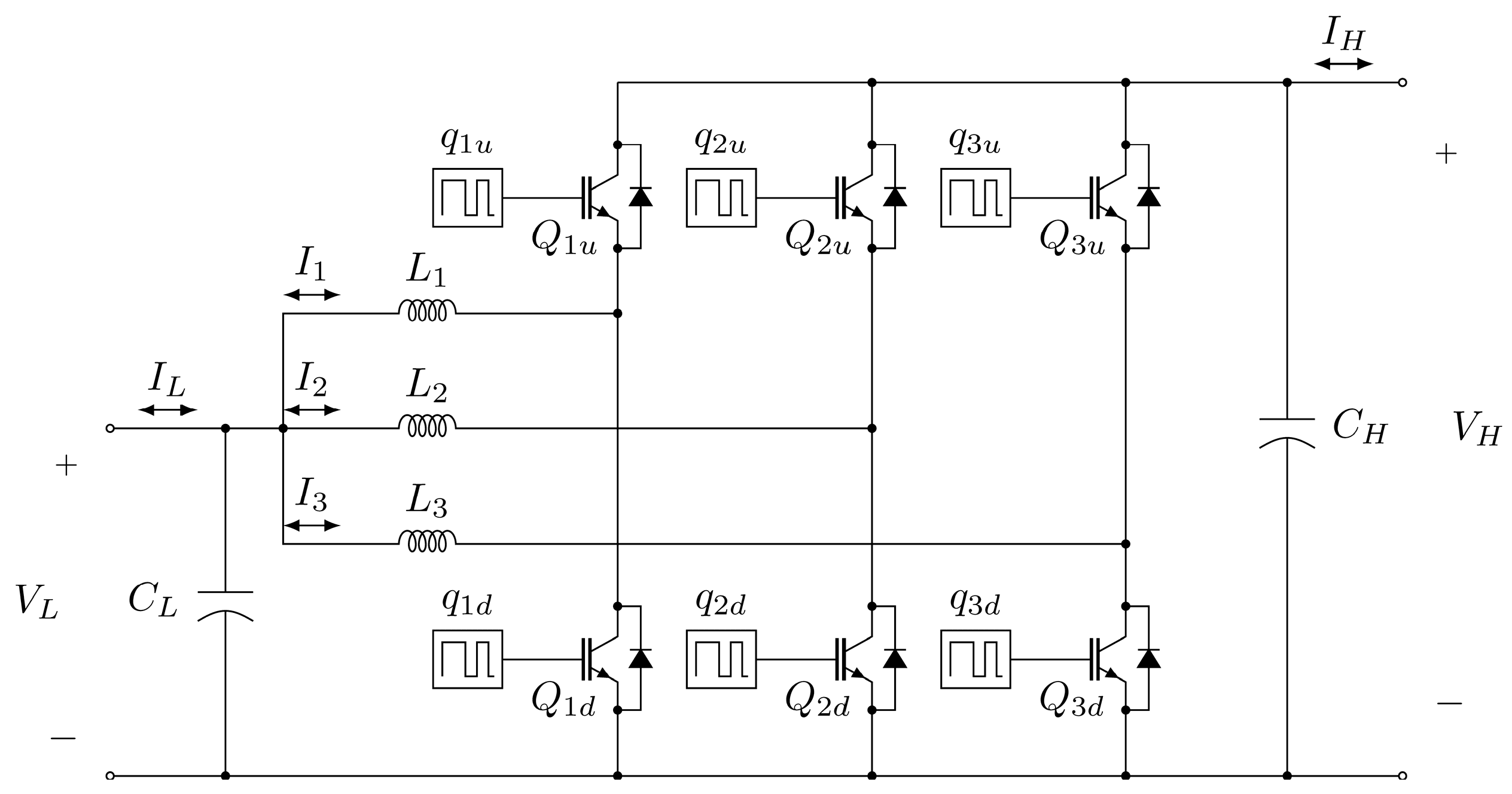
2. Converter Operation

2.1. Operation under Healthy Condition

Figure 1 depicts the three-phase non-isolated bidirectional interleaved DC-DC converter, used in this study.
The low-voltage side current IL comprises the sum of each phase current:
I L = I 1 + I 2 + I 3 .
The identical nature of all the converter phases confer a reasonable balance between them, just impaired by small deviations of phase inductances or parasitic resistances [52]. The introduction of a perturbation in one or more of the converter phases I1…3 will be reflected in the low-voltage side current IL. Considering that IL is commonly acquired by the converter controller, for both control and safety purposes, the evolution of this signal in the time-domain can be tracked, to detect abnormal behaviour of any converter phase.
The following analysis focuses on the converter operation under boost mode, i.e., with power flow taking place from the low-side to the high-side. Identical analysis is applicable to the converter operation in buck mode. An analysis will be performed for just one converter phase, due to the identical nature of the remaining phases. When a gating signal is applied on the power switch Q1d, the voltage across inductor L1 equals the low voltage VL. The current crossing the switch Q1d is equal to the current on inductor L1. Therefore, the first-order derivative of the inductor current dI1/dt will be defined as:
d I 1 d t = V L L 1 .
Hence, the slope of the current crossing inductor L1 is constant and positive, and the current increases linearly while Q1d is conducting. Consequently, the second-order derivative of the inductor current d2I1/dt2 during this period will be null:
d 2 I 1 d t 2 = 0 .
Meanwhile, when the gating signal is removed from the power switch Q1d, no current flows across it. The voltage across the inductor L1, given by the difference between the low voltage VL and the high voltage VH, is negative, as VH is higher than VL. Therefore, the first-order derivative of the current flowing through the inductor L1 is given by
d I 1 d t = V L V H L 1 .
This means that the current crossing the inductor L1 decreases linearly after the switch Q1d turn-off. Consequently, the first-order derivative dI1/dt is constant and negative immediately after the switch Q1d turn-off. This means that the second-order derivative of the inductor current d2I1/dt2 is also null when Q1d is off:
d 2 I 1 d t 2 = 0 .
According to (3) and (5), d2I1/dt2 equals to zero during the on- and off-states of the power switch Q1d. However, such statement is no longer valid for the transition between the on- and off-states (and vice-versa) of the power switch Q1d. During the transition between switch states, there is a variation in time on the absolute value of dI1/dt, that can be expressed as a linear function.
For the turn-off transition, dI1/dt can be expressed as:
d I 1 d t = V H L 1 t on off t + V L t on off + V H t i L 1 t on off
where t denotes the time variable, ton→off refers to the turn-off transition period, and ti denotes the instant at which the transition begins. Based on (6), the second-order derivative d2I1/dt2, observed during the turn-off transient of switch Q1d, is negative and given by:
d 2 I 1 d t 2 = V H L 1 t on off .
On the other hand, for the turn-on transition, dI1/dt can be expressed as follows:
d I 1 d t = V H L 1 t off on t + V L V H t off on V H t i L 1 t off on
where t denotes the time variable, toff→on refers to the turn-on transition period, and ti denotes the instant at which the transition begins. Based on (9), the second-order derivative d2I1/dt2, observed during the turn-on transient of switch Q1d, is positive and defined as:
d 2 I 1 d t 2 = V H L 1 t off on .
Two additional conditions must be considered in case that the converter operates in discontinuous conduction mode (DCM), as the phase current increases from zero during the turn-on instant. At the same time, the phase current extinguishes before the beginning of the next switching period. Considering DCM conditions, the first-order derivative dI1/dt, observed during the turn-on transient of switch Q1d, is given by:
d I 1 d t = V L L 1 t 0 on t V L t i L 1 t 0 on
where t denotes the time variable, t0→on refers to the turn-on transition period, and ti denotes the instant at which the transition begins. Hence, the second-order derivative d2I1/dt2, observed during the turn-on transient of switch Q1d, is positive and defined as:
d 2 I 1 d t 2 = V L L 1 t 0 on .
On the other hand, the first-order derivative dI1/dt, observed during the extinction of the phase current, is given by:
d I 1 d t = V H V L L 1 t off 0 t + V L V H t i + t off 0 L 1 t off 0
where t denotes the time variable, toff→0 refers to the current extinction transient period, and ti denotes the instant at which the transition begins. Hence, the second-order derivative d2I1/dt2, observed during the extinction of the phase current, is given by:
d 2 I 1 d t 2 = V H V L L 1 t off 0 .
Please note that constants ton→off, toff→on, t0→on and toff→0 mostly depend on the switching characteristics of the semiconductor devices, meaning that such parameters can usually be retrieved from the device datasheet.
From the above theoretical analysis, it is concluded that the relevant increment in the magnitude of d2I1/dt2 allows to clearly identify the effective transition between states of the power switch Q1d. Figure 2 provides a generic representation of the phase current and the corresponding first- and second-order derivatives, considering the two conduction modes: DCM and continuous conduction mode (CCM).
From Figure 2, it is shown that d2I1/dt2 clearly reflects the switching events taking place in phase 1. Particularly prominent and distinguishable increments in the magnitude of d2I1/dt2 are verified during the commutation of the power switch associated to that phase.
Since the low-voltage side current results from the sum of the three phase currents—see (1), the same is valid for the second-order derivative:
d 2 I L d t 2 = d 2 I 1 d t 2 + d 2 I 2 d t 2 + d 2 I 3 d t 2 .
As demonstrated in Figure 3, the second-order derivative of the low-voltage side current (d2IL/dt2) clearly reflects all the switching events taking place in the converter, either in DCM or CCM.

2.2. Operation under Faulty Condition

After an open-circuit (OC) fault in a power switch, no current flows through it. If the fault occurs while the power switch Q1d was on, a quick transition from the on-state to the off-state will occur, and the absolute value of the second-order derivative d2I1/dt2 will decrease substantially right after the OC fault:
d 2 I 1 d t 2 = V H L 1 t on off .
On the other hand, the increment of d2I1/dt2, expected right after a state transition on the gating signal applied to the faulty power switch Q1d, will not take place because of the likely extinction of the phase current. Therefore, d2I1/dt2 will be characterised as follows:
d 2 I 1 d t 2 = 0 .
Figure 4 shows the most important variables of the converter, during an OC fault episode. An OC fault is introduced in power switch Q1d at around half of D∙Tsw. After that moment, solid lines depict the effective evolution of the variables, whereas dashed lines represent the behaviour that would be verified for healthy operation.

2.3. Comparison between Healthy and Faulty Condition

Considering the ideal model of the interleaved converter, the voltage gain of the converter is expressed as follows:
V H V L = D M D M D
where DM denotes the period of non-zero inductor current and D denotes the switching duty cycle.
Assuming equal components in all the converter phases, it is possible to derive the general expressions of d2IL/dt2, for each state transition taking place.
For ease of analysis, the following assumptions are taken:
(1)
Considering the converter steady-state condition, it is possible to assume that variables D and DM do not suffer significant oscillations along one switching period and, consequently, these variables remain constant.
(2)
DM is always equal or higher than D. In practice, this means that condition DMD is always positive.
(3)
The turn-on and turn-off periods are assumed to be identical, resulting in the following conditions:
t 0 on t off 0 t off on t on off = t t
Based on the aforementioned assumptions, the information of second-order derivative d2IL/dt2, assessed during the transition between switch states, provides useful information about the converter condition.
Table 1 compares the second-order derivative d2IL/dt2 in the case of healthy and faulty operation, when the converter operates in boost mode. The fault condition being considered consist of an open-circuit fault in IGBT Q1d.
It is worth noting that the analysis of d2IL/dt2, presented in Table 1, is carried out exclusively during the state transitions observed in the command signal q1d. The same analysis is valid for any of the three converter phases.
An evaluation of the results provided in Table 1 allows us to draw the following conclusions:
  • For the intervals where D is variable (i.e., 0 < D < 1/3, 1/3 < D < 2/3, and 2/3 < D < 1), d2IL/dt2 approaches to zero for at least one state transition, when an OC fault occurs;
  • When D is either equal to 1/3 or 2/3, d2IL/dt2 is positive for the ON → OFF transition; under healthy state, d2IL/dt2 is either null or negative.
Given the architecture of the DC-DC converter, both boost and buck modes are feasible. For buck mode, in particular, current IL becomes negative, thus impacting the estimated values of d2IL/dt2. Table 2 compares the second-order derivative d2IL/dt2 in the case of healthy and faulty operation, when the converter operates in buck mode. The fault condition being considered consist of an open-circuit fault in IGBT Q1u.
An evaluation of the results provided in Table 2 allows us to draw the following conclusions:
  • For the intervals where D is variable (i.e., 0 < D < 1/3, 1/3 < D < 2/3, and 2/3 < D < 1), d2IL/dt2 is null for at least one state transition; these conditions are identical to those observed for the boost mode;
  • When D is either equal to 1/3 or 2/3, d2IL/dt2 is negative for the ON → OFF transition; under healthy state, d2IL/dt2 is either null or positive; these conditions are complementary to those observed for the boost mode.
As confirmed in Table 1 and Table 2, the analysis of d2IL/dt2 provides useful information about the condition of the converter semiconductors. The following section provides an explanation of the procedures taken to implement the proposed fault diagnostic strategy.

3. Proposed Fault Diagnostics Algorithm

As mentioned in Section 2, the converter left-side current IL is used for fault diagnostic purposes, as the effects of possible faults, in any of the converter phases, end up reflected in the low-voltage side current IL. Previous literature has also focused on the evaluation of IL and its evolution over time, resorting to strategies like slope analysis [5,13,14]. It is relevant to note that the proposed fault diagnostic method assures an important advantage over the diagnostic tools based on slope analysis, especially the tools applied to interleaved DC-DC converters. Considering that the diagnostic variable (input current) comprises the sum of multiple non-zero phase currents, with distinctive rising and falling slew rates overlapped in time, it is generally stated that the implementation of a diagnostic tool based on the slope analysis of the input current requires a complex and detailed analysis of many distinctive operating conditions. The adoption of a diagnostic tool based on the second-order derivative greatly simplifies the developed analysis. The overlap on time of phase current with distinctive slew rates does not impact the second-order derivative. Instead, the second-order derivative only extracts relevant information from the diagnostic variable during the switches transient states, observed as a result of the switching action.
The action of the proposed fault diagnostic solution lies on the evaluation of the magnitude of d2IL/dt2, in well-defined periods. Naturally, the computation of d2IL/dt2 involves significant processing effort. To simplify the computation process, while allowing the integration of the strategy in a DSP, d2IL/dt2 is estimated through the Euler backward approximation method, resulting in:
d 2 I L d t 2 I ¨ L = I L t 2 2 I L t 1 + I L t 0 Δ t 2
with Δ t = t 2 t 0 .
The instants t0…2 are established resorting to the gating signals applied to the converter. Figure 5 illustrates the positions of these three instants, when analysing the gating signal q1d, associated to IGBT Q1d.
Since the response of the physical system is affected by delays, delay compensation is introduced. The compensation aims to account for the delay observed between the considered gating signals and the effective beginning/ending of the conduction/blocking of the semiconductors. Such compensation is considered through careful selection of the period between instants t0…2.
To identify the faulty semiconductor, the gating signals, available in the converter controller, are used along with the information of the d2IL/dt2 to locate the faulty semiconductor. Figure 6 depicts a schematic representation of the entire fault diagnostics algorithm.

4. Simulation Results

To verify the effectiveness of the fault diagnostic algorithm proposed in this paper, simulations were carried out using MATLAB/SimulinkTM R2023a software. The converter controller is based on a dual-loop PI controller. The converter operates using an asynchronous switching pattern, which implies that only IGBTs Q1d, Q2d and Q3d are operated when the converter is in boost mode, whereas only IGBTs Q1u, Q2u and Q3u are operated when the converter is in buck mode. This system is based on a real laboratory implementation of a non-isolated bidirectional interleaved DC-DC converter.
The main parameters used in this simulation are summarised in Table 3.
The following results, which concern the converter operation in boost mode, aim to confirm the feasibility of the proposed approach in multiple operating conditions, namely in the presence of various levels of duty cycle D, conduction modes (expressed through parameter DM), and switching frequencies fsw, as well as transient state conditions.
Figure 7 depicts the evolution, in time, of the most relevant DC-DC converter and fault diagnostic variables, when the converter operates in DCM.
The converter operates in the region 0 < D < 1/3, at a switching frequency fsw of 2.5 kHz. The load resistance is 100 Ω, the phase inductance is 4 mH, and the converter output voltage VH is 70 V.
The OC fault condition, which takes place at t = 2.00036 s, translates into a noticeable unbalance in the current IL—see Figure 7b.
Referring to Figure 7c,d, which represent the second-order derivatives computed at the falling and rising edges of the gating signals, it is stated that both indicators provide accurate information about the faulty phase. Nonetheless, it is observed that faulty phase is identified quicker when evaluating the falling edges. Indeed, it is noticeable that the fault indicator computed resorting to information sampled at the falling edges (see Figure 7d) responds faster than the fault indicator computed resorting to information sampled at the rising edges (see Figure 7c). Therefore, the three diagnostic variables I ¨ L 1 I ¨ L 3 presented in the following analyses are computed around the turn-off instants of each converter phase. The diagnostic variable related to phase 1 of the converter (denoted as I ¨ L 1 in Figure 7c,d) provides relevant information about the condition of switch Q1d. Under healthy condition, I ¨ L 1 oscillates around 2 × 10 8 ; after the fault, I ¨ L 1 suddenly approaches zero, allowing an effective fault signaling at t = 2.0008 s. On the other hand, the evolution of the fault indicators related to phases 2 and 3 remains steady and unaffected by the fault. Such behaviour suggests the robustness of the approach against false positives.
Figure 8 evaluates the performance of the proposed approach for steady state condition, when the duty cycle D increases.
The converter operates in the region 1/3 < D < 2/3, at a switching frequency fsw of 2.5 kHz. The load resistance is 100 Ω, the phase inductance is 4 mH and the converter output voltage VH is 90 V.
Because of the increment in the duty cycle D, the ripple content of the current IL is greatly reduced, as seen in Figure 8b. This means that the effective diagnostic action may also reveal more demanding. As stated in Figure 8c, all three fault diagnostic indicators remain negative for healthy condition. After the OC fault in IGBT Q1d, which takes place at t = 2.00036 s, I ¨ L 1 suddenly increases to 3 × 10 8 , allowing an effective fault signaling at t = 2.00049 s. The fault is diagnosed within 130 μs, representing 32.5% of the switching period. The evolution of the three fault diagnostic variables suggests the feasibility of the proposed solution.
The good indicators of the algorithm are extended to scenarios where either boundary conduction mode (BCM) or continuous conduction mode (CCM) are observed—see Figure 9a.
The converter operates in the region 1/3 < D < 2/3, at a switching frequency fsw of 2.5 kHz. The load resistance is 50 Ω, the phase inductance is 4 mH and the converter output voltage VH is 90 V.
As stated in Figure 9c, all three fault diagnostic indicators have fairly constant negative values during healthy condition. After the OC fault in IGBT Q1d, which takes place at t = 2.00036 s, I ¨ L 1 becomes positive, allowing an effective fault signaling at t = 2.00052 s. The fault is diagnosed within 160 μs, representing 40% of the switching period.
The tests also involved an evaluation of the method at higher switching frequency. The results of the evaluation are presented in Figure 10.
The converter operates in the region 0 < D < 1/3, at a switching frequency fsw of 5 kHz. The load resistance is 100 Ω, the phase inductance is 10 mH and the converter output voltage VH is 70 V.
The increment in the switching frequency fsw, allied to the increment of the phase inductance, contribute to the smooth pattern of the current IL during healthy converter condition—see Figure 10b. Because of this, all three fault diagnostic indicators remain negative, but close to zero when the converter is healthy. After the OC fault in IGBT Q1d, which takes place at t = 2.00021 s, I ¨ L 1 suddenly increases to 0.7 × 10 8 , allowing an effective fault signaling at t = 2.00030 s. The fault is diagnosed within 90 μs.
To confirm the effectiveness under transient-state conditions, both step load change and OC fault conditions were tested in a single scenario, whose results are provided in Figure 11. In this scenario, the load resistance is changed from 100 Ω to 50 Ω, creating a load transient at the instant t = 2.5 s. Later, at t = 6.0003 s, an OC fault occurs at IGBT Q1d.
The converter operates in the region 1/3 < D < 2/3, at a switching frequency fsw of 2.5 kHz. The phase inductance is 10 mH and the converter output voltage VH is 80 V. The effect of the load transient is noticed in current IL, thanks to the increment of the current—see Figure 11a.
Referring to Figure 11b, where the three fault diagnostic variables are represented, it is noted that both load transient and OC fault impact the evolution of the diagnostic variables. Still, the differences in the evolution of these parameters are clear. While all three variables remain negative during the load transient event, the same is not observed during the OC fault event. After the OC fault in IGBT Q1d, which takes place at t = 6.00030 s, I ¨ L 1 suddenly increases to 3.1 × 10 7 , allowing an effective fault signaling at t = 6.00045 s. The fault is diagnosed within 150 μs.

5. Experimental Results

To confirm the accuracy of the simulation model and of the obtained simulation results, experimental tests were conducted on a laboratory prototype of the bidirectional interleaved DC-DC converter. The parameters of the experimental setup are the same as those reported in Table 3, which were also considered in simulation environment.
Figure 12 provides a schematic representation of the experimental setup used to test the converter operation and verify the effectiveness of the proposed fault diagnostics algorithm.
The following results address the operating conditions which have been evaluated in simulation context, i.e., steady- and transient-state conditions.
Figure 13 evaluates the performance of the proposed approach for steady-state conditions, when the converter operates in DCM.
The converter operates in the region 0 < D < 1/3, at a switching frequency fsw of 2.5 kHz. The load resistance is 100 Ω, the phase inductance is 4 mH and the converter output voltage VH is 70 V.
The condition of discontinuous conduction is clear in Figure 13a, where the phase currents momentarily reach 0 A. Likewise, Figure 13b reveals the unbalance introduced in the sum of the phase currents, introduced after the OC fault in IGBT Q1d.
The diagnostic variable related to phase 1 of the converter (denoted as I ¨ L 1 in Figure 13c,d) provides relevant information about the condition of switch Q1d. Under healthy condition, I ¨ L 1 is 1.15 × 10 8 ; after the fault, I ¨ L 1 becomes positive but nearing 0. This evolution, which aligns with the theoretical formulation provided in Table 1 for the specific combination of D and DM, allows to diagnose the fault within 80 μs, at t = 0.99865 s. Also referring to the indicators related to phases 2 and 3, it is noted that their evolution remains steady, even after the fault. This suggests the robustness of the approach against false positives.
To verify the effectiveness of the approach when the duty cycle D increases, Figure 14 evaluates the performance of the proposed approach for steady state conditions, when the converter operates in DCM.
The converter operates in the region 1/3 < D < 2/3, at a switching frequency fsw of 2.5 kHz. The load resistance is 100 Ω, the phase inductance is 4 mH and the converter output voltage VH is 90 V.
Even though DM approaches to the unitary value, the condition of discontinuous conduction is maintained in this scenario—see Figure 14a.
The diagnostic variable related to phase 1 of the converter (denoted as I ¨ L 1 in Figure 14c) provides relevant information about the condition of switch Q1d. Under healthy condition, all three diagnostic variables remain close to 2 × 10 8 ; after the fault, I ¨ L 1 remains negative but nearing 0. This evolution in the diagnostic variable allows to diagnose the fault within 200 μs, at t = 0.99910 s.
To verify the effectiveness of the approach when the converter operates in CCM, Figure 15 evaluates the performance of the proposed approach for steady state conditions.
The converter operates in the region 1/3 < D < 2/3, at a switching frequency fsw of 2.5 kHz. The load resistance is 50 Ω, the phase inductance is 4 mH and the converter output voltage VH is 90 V. In this scenario, continuous conduction mode is accomplished—see Figure 15a. The unbalance verified in the phase currents results from the asymmetry between phases and from the lack of a dedicated current balancing mechanism, which is not considered in this study. Given the non-ideal behaviour of the physical converter, associated to the presence of noise on the measurement of current IL, the unbalance between phases or other non-idealities, will translate into minor deviations of diagnostic variables from the theoretical values, tabulated in Table 1.
Like in the previous scenarios, the diagnostic variable related to phase 1 of the converter (denoted as I ¨ L 1 in Figure 15c) provides relevant information about the condition of switch Q1d. Under healthy condition, all three diagnostic variables remain close to 2 × 10 8 ; after the fault, I ¨ L 1 remains negative but nearing 0. This evolution in the diagnostic variable allows to diagnose the fault within 200 μs, at t = 0.99890 s.
The proposed approach also reveals effective when the switching frequency increases, as confirmed in Figure 16.
The converter operates in the region 0 < D < 1/3, at a switching frequency fsw of 5 kHz. The load resistance is 100 Ω, the phase inductance is 10 mH and the converter output voltage VH is 70 V. The effect of the higher switching frequency is noticed in current IL, thanks to the lower ripple amplitude and higher ripple frequency—see Figure 16a.
Like in the previous scenarios, the diagnostic variable related to phase 1 of the converter effectively flags the OC fault at switch Q1d. After the fault, I ¨ L 1 becomes positive, standing out from the other two variables. This evolution in the diagnostic variable allows to diagnose the fault within 280 μs, at t = 0.99939 s.
To confirm the effectiveness under transient state condition, both step load change and OC fault conditions are tested in a single scenario, whose results are provided in Figure 17. In this scenario, the load resistance is changed from 100 Ω to 50 Ω, creating a load transient at the instant t = 2.5 s. Later, at t = 5.99401 s, an OC fault occurs at IGBT Q1d.
The converter operates in the region 1/3 < D < 2/3, at a switching frequency fsw of 2.5 kHz. The phase inductance is 10 mH and the converter output voltage VH is 80 V. The effect of the load transient is noticed in current IL, thanks to the increment of the current—see Figure 17a.
Referring to Figure 17b, it is noted that all three diagnostic variables approach to zero, because of the load transient condition. This behaviour does not compromise the effectiveness of the solution, since the sign of the diagnostic variables remains negative. Indeed, when looking at the evolution of the duty cycle D, shown in Figure 17d, it is noted that this parameter approaches 1/3. Under such circumstance, the proposed fault diagnostic approach applies the exception that allows to fulfil the conditions expressed in Table 1 for cases where D approaches 1/3 and 2/3. Accordingly, no fault diagnostic flags are triggered.
Referring to Figure 17c, it is observed that I ¨ L 1 becomes positive, standing out from the other two fault diagnostic variables, at t = 5.99425 s.

Comparison with the State of the Art

Table 4 compiles information considered useful in evaluating the performance of the fault diagnostic algorithms available in the literature, particularly those intended for DC-DC converters. It is worth noting that the performance metrics shown in Table 4 solely take into consideration the data provided by the authors in their corresponding communications.
As stated in Table 4, the proposed diagnostic strategy provides remarkable capabilities to diagnose faults in a short period of time, while requesting a small computational effort. When compared to the state-of-the-art fault diagnostic strategies, the proposed diagnostic strategy reaches one of the lowest ratios between the maximum fault diagnostic time and sampling time. Such performance lies on the fact that the proposed fault diagnostic algorithm resorts to simple manipulation of the converter variables and their values, without requiring complex mathematical computations or emulation of the converter model.

6. Conclusions

The adoption of DC-DC converters is becoming increasingly important. Historically, DC-DC converters were mainly dedicated to industrial applications. However, these converters may become part of office equipment and home appliances soon, due to the increasing interest in DC microgrids for residential and offices buildings. In this context, ensuring high reliability and availability of power conversion solutions is of utmost importance. Therefore, significant attention should be paid to fault diagnostics in DC-DC power converters.
This paper presented a new fault diagnostic strategy capable of effectively diagnosing OC faults in the power switches of a multiphase non-isolated DC-DC converter. An approximation of the second-order derivative is applied to the converter input current, aiming to obtain fault signatures suitable to diagnose faults in any of the converter phases. Since the method synchronises the instants for sampling the converter input current with the gating signals, the risk of false fault alarms is obviated for the entire operating range of the converter. In addition, the synchronisation feature applied to the sampling operation promotes the effective diagnosis for converters with a high number of phases. The simplicity of the method also enables its transposition to many other DC-DC converter topologies.
Another advantage of the proposed approach is its ease of integration with existing control units. Because the proposed method only requires variables typically available as inputs or outputs of the control system (converter input current IL, duty cycle D and gating signals), it can be implemented without altering the control architecture or extracting internal variables of the controller.

Author Contributions

Conceptualization, F.B. and A.J.M.C.; methodology, F.B. and A.J.M.C.; software, F.B. and A.J.M.C.; validation, F.B. and A.J.M.C.; formal analysis, F.B. and A.J.M.C.; investigation, F.B. and A.J.M.C.; resources, A.J.M.C.; data curation, F.B.; writing—original draft preparation, F.B.; writing—review and editing, A.J.M.C.; visualization, F.B. and A.J.M.C.; supervision, A.J.M.C.; project administration, A.J.M.C.; funding acquisition, A.J.M.C. All authors have read and agreed to the published version of the manuscript.

Funding

This work was supported by the Portuguese Foundation for Science and Technology (FCT) under Projects UIDB/04131/2020 and UIDP/04131/2020.

Data Availability Statement

Data are contained within the article.

Conflicts of Interest

The authors declare no conflicts of interest.

References

  1. Evolution of Households Energy Consumption Patterns across the EU. Available online: https://www.enerdata.net/publications/executive-briefing/households-energy-efficiency.html (accessed on 28 September 2022).
  2. Bento, F.; Ribeiro, E. DC-DC Converters. In Diagnosis and Fault Tolerance of Electric Machines, Power Electronics and Drives; Marques Cardoso, A.J., Ed.; IET: Hertfordshire, UK, 2018; ISBN 978-1-78561-531-3. [Google Scholar]
  3. Bento, F.; Marques Cardoso, A.J. A Comprehensive Survey on Fault Diagnosis and Fault Tolerance of DC-DC Converters. Chin. J. Electr. Eng. 2018, 4, 1–12. [Google Scholar] [CrossRef]
  4. Kumar, G.K.; Elangovan, D. Review on Fault-Diagnosis and Fault-Tolerance for DC-DC Converters. IET Power Electron. 2020, 13, 1–13. [Google Scholar] [CrossRef]
  5. Park, K.; Chen, Z. Open-Circuit Fault Detection and Tolerant Operation for a Parallel-Connected SAB DC–DC Converter. In Proceedings of the 2014 IEEE Applied Power Electronics Conference and Exposition—APEC 2014, Fort Worth, TX, USA, 16–20 March 2014; pp. 1966–1972. [Google Scholar]
  6. Ribeiro, E.; Cardoso, A.J.M.; Boccaletti, C. Open-Circuit Fault Diagnosis in Interleaved DC-DC Converters. IEEE Trans. Power Electron. 2014, 29, 3091–3102. [Google Scholar] [CrossRef]
  7. Jamshidpour, E.; Poure, P.; Saadate, S. Photovoltaic Systems Reliability Improvement by Real-Time FPGA-Based Switch Failure Diagnosis and Fault-Tolerant DC-DC Converter. IEEE Trans. Ind. Electron. 2015, 62, 7247–7255. [Google Scholar] [CrossRef]
  8. Kamel, T.; Biletskiy, Y.; Chang, L. Real-Time Diagnosis for Open-Circuited and Unbalance Faults in Electronic Converters Connected to Residential Wind Systems. IEEE Trans. Ind. Electron. 2016, 63, 1781–1792. [Google Scholar] [CrossRef]
  9. Bento, F.; Cardoso, A.J.M. Fault Diagnosis in DC-DC Converters Using a Time-Domain Analysis of the Reference Current Error. In Proceedings of the IECON 2017—43rd Annual Conference of the IEEE Industrial Electronics Society, Beijing, China, 29 October–1 November 2017; pp. 5060–5065. [Google Scholar]
  10. Ribeiro, E.; Cardoso, A.J.M.; Boccaletti, C. Fault Diagnosis in Unidirectional Non-Isolated DC–DC Converters. In Proceedings of the 2014 IEEE Energy Conversion Congress and Exposition (ECCE), Pittsburgh, PA, USA, 14–18 September 2014; pp. 1140–1145. [Google Scholar]
  11. Li, C.; Yu, Y.; Tang, T.; Liu, Q.; Peng, X. A Robust Open-Circuit Fault Diagnosis Method for Three-Phase Interleaved Boost Converter. IEEE Trans. Power Electron. 2022, 37, 11187–11198. [Google Scholar] [CrossRef]
  12. Zandi, O.; Poshtan, J. A Novel Algorithm for Open Switch Fault Detection and Fault Tolerant Control of Interleaved DC-DC Boost Converters. IET Power Electron. 2024, 17, 721–730. [Google Scholar] [CrossRef]
  13. Bento, F.; Cardoso, A.J.M. Open-Circuit Fault Diagnosis and Fault Tolerant Operation of Interleaved DC-DC Boost Converters for Homes and Offices. IEEE Trans. Ind. Appl. 2019, 55, 4855–4864. [Google Scholar] [CrossRef]
  14. Farjah, E.; Givi, H.; Ghanbari, T. Application of an Efficient Rogowski Coil Sensor for Switch Fault Diagnosis and Capacitor ESR Monitoring in Nonisolated Single-Switch DC–DC Converters. IEEE Trans. Power Electron. 2017, 32, 1442–1456. [Google Scholar] [CrossRef]
  15. Bento, F.; Cardoso, A.J.M. Fault Tolerant DC-DC Converters in DC Microgrids. In Proceedings of the 2017 IEEE Second International Conference on DC Microgrids (ICDCM), Nuremberg, Germany, 27–29 June 2017; pp. 484–490. [Google Scholar]
  16. Muhammed Ramees, M.K.P.; Ahmad, M.W. An Integrated Approach for Current Balancing and Open-Circuit Fault Diagnosis for Interleaved Boost Converter. IEEE Trans. Ind. Electron. 2024, 71, 13310–13318. [Google Scholar] [CrossRef]
  17. Ribeiro, E.; Cardoso, A.J.M.; Boccaletti, C. Fault-Tolerant Strategy for a Photovoltaic DC–DC Converter. IEEE Trans. Power Electron. 2013, 28, 3008–3018. [Google Scholar] [CrossRef]
  18. Sheng, H.; Wang, F.; Tipton IV, C.W. A Fault Detection and Protection Scheme for Three-Level DC–DC Converters Based on Monitoring Flying Capacitor Voltage. IEEE Trans. Power Electron. 2012, 27, 685–697. [Google Scholar] [CrossRef]
  19. Bi, K.; An, Q.; Duan, J.; Sun, L.; Gai, K. Fast Diagnostic Method of Open Circuit Fault for Modular Multilevel DC/DC Converter Applied in Energy Storage System. IEEE Trans. Power Electron. 2017, 32, 3292–3296. [Google Scholar] [CrossRef]
  20. Chen, Y.; Pei, X.; Nie, S.; Kang, Y. Monitoring and Diagnosis for the DC–DC Converter Using the Magnetic Near Field Waveform. IEEE Trans. Ind. Electron. 2011, 58, 1634–1647. [Google Scholar] [CrossRef]
  21. Li, P.; Li, X.; Zeng, T. A Fast and Simple Fault Diagnosis Method for Interleaved DC-DC Converters Based on Output Voltage Analysis. Electronics 2021, 10, 1451. [Google Scholar] [CrossRef]
  22. Li, C.; Yu, Y.; Yang, Z.; Wang, W.; Peng, X. A Sensorless Open-Circuit Fault Identification Method for Interleaved Boost Converter. IEEE Trans. Instrum. Meas. 2024, 73, 3525508. [Google Scholar] [CrossRef]
  23. Nie, S.; Pei, X.; Chen, Y.; Kang, Y. Fault Diagnosis of PWM DC–DC Converters Based on Magnetic Component Voltages Equation. IEEE Trans. Power Electron. 2014, 29, 4978–4998. [Google Scholar] [CrossRef]
  24. Givi, H.; Farjah, E.; Ghanbari, T. A Comprehensive Monitoring System for Online Fault Diagnosis and Aging Detection of Non-Isolated DC–DC Converters’ Components. IEEE Trans. Power Electron. 2019, 34, 6858–6875. [Google Scholar] [CrossRef]
  25. Givi, H.; Farjah, E.; Ghanbari, T. Switch and Diode Fault Diagnosis in Non-Isolated DC–DC Converters Using Diode Voltage Signature. IEEE Trans. Ind. Electron. 2018, 65, 1606–1615. [Google Scholar] [CrossRef]
  26. Ahmad, M.W.; Gorla, N.B.Y.; Malik, H.; Panda, S.K. A Fault Diagnosis and Postfault Reconfiguration Scheme for Interleaved Boost Converter in PV-Based System. IEEE Trans. Power Electron. 2021, 36, 3769–3780. [Google Scholar] [CrossRef]
  27. Wang, Y.; Guan, Y.; Molinas, M.; Fosso, O.B.; Hu, W.; Zhang, Y. Open-Circuit Switching Fault Analysis and Tolerant Strategy for Dual-Active-Bridge DC–DC Converter Considering Parasitic Parameters. IEEE Trans. Power Electron. 2022, 37, 15020–15034. [Google Scholar] [CrossRef]
  28. Rastogi, S.K.; Shah, S.S.; Singh, B.N.; Bhattacharya, S. Vector-Based Open-Circuit Fault Diagnosis Technique for a Three-Phase DAB Converter. IEEE Trans. Ind. Electron. 2024, 71, 8207–8211. [Google Scholar] [CrossRef]
  29. Mahdavi, M.S.; Karimzadeh, M.S.; Rahimi, T.; Gharehpetian, G.B. A Fault-Tolerant Bidirectional Converter for Battery Energy Storage Systems in DC Microgrids. Electronics 2023, 12, 679. [Google Scholar] [CrossRef]
  30. Han, W.; Cheng, L.; Han, W.; Yu, C.; Hao, Z.; Yin, Z. Soft Fault Diagnosis for DC–DC Converter Based on Improved ResNet-50. IEEE Access 2023, 11, 81157–81168. [Google Scholar] [CrossRef]
  31. Espinoza-Trejo, D.R.; Castro, L.M.; Bárcenas, E.; Sánchez, J.P. Data-Driven Switch Fault Diagnosis for DC/DC Boost Converters in Photovoltaic Applications. IEEE Trans. Ind. Electron. 2024, 71, 1631–1640. [Google Scholar] [CrossRef]
  32. Hang, J.; Ge, C.; Ding, S.; Li, W.; Huang, Y.; Hua, W. A Global State Observer-Based Open-Switch Fault Diagnosis for Bidirectional DC–DC Converters in Hybrid Energy Source System. IEEE Trans. Power Electron. 2023, 38, 13085–13098. [Google Scholar] [CrossRef]
  33. Ding, S.; Tang, D.; Hang, J.; Zhao, J.; Gui, S. Robust Open-Switch Fault Diagnosis of Bidirectional DC/DC Converters Based on Extended Kalman Filter With Multiple Corrections. IEEE Trans. Circuits Syst. Regul. Pap. 2024, 71, 4363–4374. [Google Scholar] [CrossRef]
  34. Rastogi, S.K.; Shah, S.S.; Singh, B.N.; Bhattacharya, S. Mode Analysis, Transformer Saturation, and Fault Diagnosis Technique for an Open-Circuit Fault in a Three-Phase DAB Converter. IEEE Trans. Power Electron. 2023, 38, 7644–7660. [Google Scholar] [CrossRef]
  35. Yang, W.; Ma, J.; Zhu, M.; Hu, C. Open-Circuit Fault Diagnosis and Tolerant Method of Multiport Triple Active-Bridge DC-DC Converter. IEEE Trans. Ind. Appl. 2023, 59, 5473–5487. [Google Scholar] [CrossRef]
  36. Wassinger, N.; Penovi, E.; Retegui, R.G.; Maestri, S. Open-Circuit Fault Identification Method for Interleaved Converters Based on Time-Domain Analysis of the State Observer Residual. IEEE Trans. Power Electron. 2019, 34, 3740–3749. [Google Scholar] [CrossRef]
  37. Poon, J.; Jain, P.; Konstantakopoulos, I.C.; Spanos, C.; Panda, S.K.; Sanders, S.R. Model-Based Fault Detection and Identification for Switching Power Converters. IEEE Trans. Power Electron. 2017, 32, 1419–1430. [Google Scholar] [CrossRef]
  38. Zhuo, S.; Gaillard, A.; Xu, L.; Liu, C.; Paire, D.; Gao, F. An Observer-Based Switch Open-Circuit Fault Diagnosis of DC-DC Converter for Fuel Cell Application. IEEE Trans. Ind. Appl. 2020, 56, 3159–3167. [Google Scholar] [CrossRef]
  39. Jain, P.; Jian, L.; Poon, J.; Spanos, C.; Sanders, S.R.; Xu, J.-X.; Panda, S.K. A Luenberger Observer-Based Fault Detection and Identification Scheme for Photovoltaic DC-DC Converters. In Proceedings of the IECON 2017—43rd Annual Conference of the IEEE Industrial Electronics Society, Beijing, China, 1 October 2017; pp. 5015–5020. [Google Scholar]
  40. Zhuo, S.; Xu, L.; Gaillard, A.; Huangfu, Y.; Paire, D.; Gao, F. Robust Open-Circuit Fault Diagnosis of Multi-Phase Floating Interleaved DC–DC Boost Converter Based on Sliding Mode Observer. IEEE Trans. Transp. Electrif. 2019, 5, 638–649. [Google Scholar] [CrossRef]
  41. Xu, L.; Ma, R.; Xie, R.; Xu, J.; Huangfu, Y.; Gao, F. Open-Circuit Switch Fault Diagnosis and Fault-Tolerant Control for Output-Series Interleaved Boost DC–DC Converter. IEEE Trans. Transp. Electrif. 2021, 7, 2054–2066. [Google Scholar] [CrossRef]
  42. Su, Q.; Wang, Z.; Xu, J.; Li, C.; Li, J. Fault Detection for DC-DC Converters Using Adaptive Parameter Identification. J. Frankl. Inst. 2022, 359, 5778–5797. [Google Scholar] [CrossRef]
  43. Poon, J.; Jain, P.; Spanos, C.; Panda, S.K.; Sanders, S.R. Fault Prognosis for Power Electronics Systems Using Adaptive Parameter Identification. IEEE Trans. Ind. Appl. 2017, 53, 2862–2870. [Google Scholar] [CrossRef]
  44. Pazouki, E.; De Abreu-Garcia, J.A.; Sozer, Y. Short Circuit Fault Diagnosis for Interleaved DC–DC Converter Using DC-Link Current Emulator. In Proceedings of the 2017 IEEE Applied Power Electronics Conference and Exposition (APEC), Tampa, FL, USA, 26–30 March 2017; pp. 230–236. [Google Scholar]
  45. Pazouki, E.; Sozer, Y.; De Abreu-Garcia, J.A. Fault Diagnosis and Fault Tolerant Operation of Non-Isolated DC–DC Converter. IEEE Trans. Ind. Appl. 2018, 54, 310–320. [Google Scholar] [CrossRef]
  46. Jain, P.; Poon, J.; Singh, J.P.; Spanos, C.; Sanders, S.R.; Panda, S.K. A Digital Twin Approach for Fault Diagnosis in Distributed Photovoltaic Systems. IEEE Trans. Power Electron. 2020, 35, 940–956. [Google Scholar] [CrossRef]
  47. Jiang, Y.; Xia, L.; Zhang, J. A Fault Feature Extraction Method for DC–DC Converters Based on Automatic Hyperparameter-Optimized 1-D Convolution and Long Short-Term Memory Neural Networks. IEEE J. Emerg. Sel. Top. Power Electron. 2022, 10, 4703–4714. [Google Scholar] [CrossRef]
  48. Ren, T.; Han, T.; Guo, Q.; Li, G. Analysis of Interpretability and Generalizability for Power Converter Fault Diagnosis Based on Temporal Convolutional Networks. IEEE Trans. Instrum. Meas. 2023, 72, 3518511. [Google Scholar] [CrossRef]
  49. Liu, Y.; Zhang, G.; Miao, J.; Zhao, Z.; Yin, Q.; Zhao, J. Fault Diagnosis of DC/DC Buck Converter for Embedded Applications Based on BO-ELM. IEEE Trans. Ind. Electron. 2024, 71, 15034–15043. [Google Scholar] [CrossRef]
  50. Jia, Z.; Liu, Z.; Vong, C.-M.; Wang, S.; Cai, Y. DC-DC Buck Circuit Fault Diagnosis with Insufficient State Data Based on Deep Model and Transfer Strategy. Expert Syst. Appl. 2023, 213, 118918. [Google Scholar] [CrossRef]
  51. Miao, J.; Liu, Y.; Yin, Q.; Ju, B.; Zhang, G.; Wang, H. A Novel Soft Fault Detection and Diagnosis Method for a DC/DC Buck Converter Based on Contrastive Learning. IEEE Trans. Power Electron. 2024, 39, 1501–1513. [Google Scholar] [CrossRef]
  52. Ni, L.; Patterson, D.J.; Hudgins, J.L. High Power Current Sensorless Bidirectional 16-Phase Interleaved DC–DC Converter for Hybrid Vehicle Application. IEEE Trans. Power Electron. 2012, 27, 1141–1151. [Google Scholar] [CrossRef]
Figure 1. Three-phase non-isolated bidirectional interleaved DC-DC converter.
Electronics 13 03778 g001
Figure 2. Phase 1 control pulse q1d, phase 1 inductor current I1, first- and second-order derivatives of phase 1 inductor current (dI1/dt and d2I1/dt2, respectively), considering the following conduction modes: (a) DCM; (b) CCM.
Electronics 13 03778 g002
Figure 3. Individual phase currents I1…3, low-voltage side current IL, first- and second-order derivatives of current IL (dIL/dt and d2IL/dt2, respectively), considering the following conduction modes: (a) DCM; (b) CCM.
Electronics 13 03778 g003
Figure 4. Phase 1 control pulse q1d, phase 1 inductor current I1, first- and second-order derivatives of phase 1 inductor current (dI1/dt and d2I1/dt2, respectively), observed in the presence of an OC fault in IGBT Q1d.
Electronics 13 03778 g004
Figure 5. Identification of the instants for sampling the current IL.
Electronics 13 03778 g005
Figure 6. Schematic representation of the proposed fault diagnostics algorithm.
Electronics 13 03778 g006
Figure 7. Evolution of the most relevant converter variables when an OC fault occurs in power switch Q1d, at t = 2.00036 s: (a) phase currents I1…3; (b) low-voltage side current IL; (c) second-order derivatives IL1…3, computed at the rising edges of the gating signals; (d) second-order derivatives IL1…3, computed at the falling edges of the gating signals.
Electronics 13 03778 g007
Figure 8. Evolution of the most relevant converter variables when OC fault occurs in power switch Q1d, at t = 2.00036 s: (a) phase currents I1…3; (b) low-voltage side current IL; (c) second-order derivatives IL1…3, computed at the falling edges of the gating signals.
Electronics 13 03778 g008
Figure 9. Evolution of the most relevant converter variables when OC fault occurs in power switch Q1d, at t = 2.00036 s: (a) phase currents I1…3; (b) low-voltage side current IL; (c) second-order derivatives IL1…3, computed at the falling edges of the gating signals.
Electronics 13 03778 g009aElectronics 13 03778 g009b
Figure 10. Evolution of the most relevant converter variables when OC fault occurs in power switch Q1d, at t = 2.00021 s: (a) low-voltage side current IL; (b) second-order derivatives IL1…3, computed at the falling edges of the gating signals.
Electronics 13 03778 g010
Figure 11. Evolution of the most relevant converter variables when OC fault occurs in power switch Q1d, at t = 6.0003 s: (a) low-voltage side current IL; (b) second-order derivatives IL1…3, computed at the falling edges of the gating signals; (c) zoomed view of the second-order derivatives IL1…3 around the OC fault instant.
Electronics 13 03778 g011
Figure 12. Schematic of the experimental assembly.
Electronics 13 03778 g012
Figure 13. Evolution of the most relevant converter variables when an OC fault occurs in power switch Q1d, at t = 0.99857 s: (a) phase currents I1…3; (b) low-voltage side current IL; (c) second-order derivatives IL1…3, computed at the falling edges of the gating signals; (d) second-order derivatives IL1…3, computed at the rising edges of the gating signals.
Electronics 13 03778 g013
Figure 14. Evolution of the most relevant converter variables when OC fault occurs in power switch Q1d, at t = 0.99890 s: (a) phase currents I1…3; (b) low-voltage side current IL; (c) second-order derivatives IL1…3, computed at the falling edges of the gating signals.
Electronics 13 03778 g014
Figure 15. Evolution of the most relevant converter variables when OC fault occurs in power switch Q1d, at t = 0.99870 s: (a) phase currents I1…3; (b) low-voltage side current IL; (c) second-order derivatives IL1…3, computed at the falling edges of the gating signals.
Electronics 13 03778 g015
Figure 16. Evolution of the most relevant converter variables when OC fault occurs in power switch Q1d, at t = 0.99911 s: (a) low-voltage side current IL; (b) second-order derivatives IL1…3, computed at the falling edges of the gating signals.
Electronics 13 03778 g016aElectronics 13 03778 g016b
Figure 17. Evolution of the most relevant converter variables when OC fault occurs in power switch Q1d, at t = 5.99461 s: (a) low-voltage side current IL; (b) second-order derivatives IL1…3, computed at the falling edges of the gating signals; (c) zoomed view of the second-order derivatives IL1…3 around the OC fault instant; (d) duty cycle D.
Electronics 13 03778 g017
Table 1. Second-order derivative of the low-voltage side current IL (steady state)—boost mode.
DDMq1d State
Transition
d 2 I L / d t 2 ,
Healthy
d 2 I L / d t 2 ,
Faulty
0 < D < 1 3 D M = 1 3
D M = 2 3
OFF → ON V H L t t > 0 V H V L L t t > 0
ON → OFF V H L t t < 0 0
D M = 1
(BCM and CCM)
OFF → ON V H L t t > 0 0
ON → OFF V H L t t < 0 0
0 < D M < 1 3
1 3 < D M < 2 3
2 3 < D M < 1
OFF → ON V L L t t > 0 0
ON → OFF V H L t t < 0 0
D M = 1 3 + D
D M = 2 3 + D
OFF → ON V L L t t > 0 0
ON → OFF V L L t t < 0 V H V L L t t > 0
D = 1 3 D M = 2 3 OFF → ON 0 V L L t t < 0
ON → OFF 0 V H L t t > 0
D M = 1
(BCM and CCM)
OFF → ON 0 V H L t t < 0
ON → OFF 0 V L L t t > 0
1 3 < D M < 2 3
2 3 < D M < 1
OFF → ON V L V H L t t < 0 V H L t t < 0
ON → OFF V L V H L t t < 0 V L L t t > 0
1 3 < D < 2 3 D M = 2 3 OFF → ON V H L t t > 0 V H V L L t t > 0
ON → OFF V H L t t < 0 0
D M = 1
(BCM and CCM)
OFF → ON V H L t t > 0 0
ON → OFF V H L t t < 0 0
1 3 < D M < 2 3
2 3 < D M < 1
OFF → ON V L L t t > 0 0
ON → OFF V H L t t < 0 0
D M = 1 3 + D OFF → ON V L L t t > 0 0
ON → OFF V L L t t < 0 V H V L L t t > 0
D = 2 3 D M = 1
(BCM and CCM)
OFF → ON 0 V H L t t < 0
ON → OFF 0 V H L t t > 0
2 3 < D M < 1 OFF → ON V L V H L t t < 0 V H L t t < 0
ON → OFF V L V H L t t < 0 V L L t t > 0
2 3 < D < 1 D M = 1
(BCM and CCM)
OFF → ON V H L t t > 0 0
ON → OFF V H L t t < 0 0
2 3 < D M < 1 OFF → ON V L L t t > 0 0
ON → OFF V H L t t < 0 0
Table 2. Second-order derivative of the low-voltage side current IL (steady state)—buck mode.
DDMq1u State
Transition
d 2 I L / d t 2 ,
Healthy
d 2 I L / d t 2 ,
Faulty
0 < D < 1 3 D M = 1 3
D M = 2 3
OFF → ON V H L t t < 0 V L L t t > 0
ON → OFF V H L t t > 0 0
D M = 1
(BCM and CCM)
OFF → ON V H L t t < 0 0
ON → OFF V H L t t > 0 0
0 < D M < 1 3
1 3 < D M < 2 3
2 3 < D M < 1
OFF → ON V L V H L t t < 0 0
ON → OFF V H L t t > 0 0
D M = 1 3 + D
D M = 2 3 + D
OFF → ON V L V H L t t < 0 0
ON → OFF V H V L L t t > 0 V L L t t < 0
D = 1 3 D M = 2 3 OFF → ON 0 V H V L L t t > 0
ON → OFF 0 V H L t t < 0
D M = 1
(BCM and CCM)
OFF → ON 0 V H L t t > 0
ON → OFF 0 V H L t t < 0
1 3 < D M < 2 3
2 3 < D M < 1
OFF → ON V L L t t > 0 V H L t t > 0
ON → OFF V L L t t > 0 V L V H L t t < 0
1 3 < D < 2 3 D M = 2 3 OFF → ON V H L t t < 0 V L L t t > 0
ON → OFF V H L t t > 0 0
D M = 1
(BCM and CCM)
OFF → ON V H L t t < 0 0
ON → OFF V H L t t > 0 0
1 3 < D M < 2 3
2 3 < D M < 1
OFF → ON V L V H L t t < 0 0
ON → OFF V H L t t > 0 0
D M = 1 3 + D OFF → ON V L V H L t t < 0 0
ON → OFF V H V L L t t > 0 V L L t t < 0
D = 2 3 D M = 1
(BCM and CCM)
OFF → ON 0 V H L t t > 0
ON → OFF 0 V H L t t < 0
2 3 < D M < 1 OFF → ON V H L t t > 0 V H L t t > 0
ON → OFF V H L t t > 0 V L V H L t t < 0
2 3 < D < 1 D M = 1
(BCM and CCM)
OFF → ON V H L t t < 0 0
ON → OFF V H L t t > 0 0
2 3 < D M < 1 OFF → ON V L V H L t t < 0 0
ON → OFF V H L t t > 0 0
Table 3. System parameters.
Left-side voltage (VL)48 V
Right-side voltage (VH){70, 90} V
Inductance (Li){4, 10} mH
Output capacitance (CH)680 μF
Load resistance (RL){50, 100} Ω
Switching frequency (fsw){2.5, 5} kHz
Simulation sampling time (Ts)5 μs
Table 4. Comparative analysis of the fault diagnostic strategies available in the literature.
Ref. Target Converter TopologiesDiagnostic Variablefsw(1)Ts(2)td_max(3)td_max/Ts(4)
[17]DC-DC converters for PV applicationsPV variables5 kHz50 μs250 ms5000
[6]Interleaved boost converterInput current derivative sign1 kHz25 μs, 50 μs2 Tsw (5) (2 ms)40
[44,45]Non-isolated DC-DC converters Inductor current emulation{10, 20} kHz10 μsTsw (100 μs, 50 μs)5
[37]Switching power convertersState estimation10 to 20 kHz100 μs10 ms100
[43]Interleaved boost convertersParameter identification10 kHz10 μsTsw (100 μs)10
[13]Interleaved boost convertersInput current slope{1, 3, 5} kHz20 μs2 Tsw (400 μs)20
[11]Interleaved boost convertersInput current sampling20 kHz16.7 μs2 Tsw (100 μs)6
[24,25]Non-isolated DC-DC convertersDiode voltage monitoring50 kHz-Tsw (20 μs)-
[39]Boost convertersLuenberger observer10 kHz10 μsTsw (100 μs)10
[36]Interleaved buck convertersState observer25 kHz0.67 μs2 Tsw (80 μs)119.4
[41]IPOS boost convertersI&I observer for input voltage25 kHz20 μs2 Tsw (80 μs)4
[46]Four-switch buck-boost converterDigital twin50 kHz2 μs201 Tsw (4.03 ms)2015
Proposed Bidirectional interleaved convertersSecond-order current derivative{2.5, 5} kHz20 μsTsw (200 μs)10
Nomenclature: (1) fsw—switching frequency; (2) Ts—fault signatures sampling time; (3) td_max—maximum fault diagnostic time; (4) td_max/Ts—lowest ratio between maximum fault diagnostic time and sampling time; (5) Tsw—switching period (Tsw = 1/fsw).
Disclaimer/Publisher’s Note: The statements, opinions and data contained in all publications are solely those of the individual author(s) and contributor(s) and not of MDPI and/or the editor(s). MDPI and/or the editor(s) disclaim responsibility for any injury to people or property resulting from any ideas, methods, instructions or products referred to in the content.

