Article

An 88 dB SNDR 100 kHz BW Sturdy MASH Delta-Sigma Modulator Using Self-Cascoded Floating Inverter Amplifiers

1
College of Information Science and Electronics Engineering, Zhejiang University, Hangzhou 310027, China
2
Beijing Smartchip Microelectronics Technology Company Limited, Beijing 100192, China
*
Author to whom correspondence should be addressed.
Electronics 2024, 13(19), 3865; https://doi.org/10.3390/electronics13193865 (registering DOI)
Submission received: 15 August 2024 / Revised: 19 September 2024 / Accepted: 24 September 2024 / Published: 29 September 2024
(This article belongs to the Special Issue Analog and Mixed Circuit: Design and Applications)

Abstract

:
Battery-powered Internet-of-Things applications require high-resolution, energy-efficient analog-to-digital converters (ADCs). There are still limited works on sub-MHz-bandwidth ADC designs. This paper presents a sturdy multi-stage shaping (SMASH) discrete-time (DT) delta-sigma modulator (DSM) structure using a self-cascoded floating-inverter-based dynamic amplifier (FIA). The proposed structure removes the explicit quantization error extraction of the first loop and all the feedback DACs in the cascaded loop, decreasing the design complexity of the circuit. This enables the proposed DT DSM to operate at a higher speed, which is suitable for achieving high-order noise at a low oversampling ratio (OSR). The proposed self-cascoded FIA is more power-efficient and can acquire more than 45 dB DC gain under a 1.2 V supply. The DT DSM implemented in a piece of 55 nm CMOS technology measures an 88.0 dB peak signal-to-noise-and-distortion ratio (SNDR) in a 100 kHz bandwidth (BW) and an 85.3 dB dynamic range (DR), consuming 249.1 μW from a 1.2 V supply at 10 MS/s. The obtained 174.0 dB SNDR-based Schreier figure-of-merit (FoMs) is competitive within state-of-art high-resolution (SNDR > 85 dB) and general-purpose (sub-MHz-bandwidth) ΔΣ ADCs.

1. Introduction

1.1. Background

Ubiquitous smart sensory systems require sub-MHz-bandwidth analog-to-digital converters (ADCs) with high resolution and excellent power efficiency. Generally, the key applications of these sensors demand ADCs with a SNR exceeding 85 dB and a bandwidth of hundreds of kHz. However, for sub-MHz-bandwidth ADCs, a low sampling frequency results in a small oversampling ratio (OSR), thus limiting the achievable resolution of discrete-time (DT) delta-sigma modulators (DSMs). It is unrealistic to blindly increase the quantizer bits as the digital-to-analog converter (DAC) complexity would exponentially increase the power and area. High-order single-loop DSMs are prone to instability, decreasing the achievable high maximum stable amplitude (MSA) [1]. Multi-stage noise shaping (MASH) topology can achieve high-order noise-shaping while avoiding stability issues. However, due to the strict requirement of high DC gain in the integrators, achieving low power is difficult while minimizing the leakage of the first-stage quantization error [2,3]. To overcome these disadvantages, a compelling alternative to MASH is the sturdy MASH (SMASH). They can achieve the same noise-shaping properties without any matching requirements between the analog and digital filters, which significantly eases the stress of the integrators [4]. Therefore, SMASH ADCs offer good immunity to circuit imperfections and non-idealities, making them robust and suitable for practical applications.

1.2. Literature Review

In [4], a DT 2-2 SMASH is proposed with an OSR of only 16. It achieves a maximum stable amplitude (MSA) of −1.5 dBFs while performing fourth-order noise shaping. A 35 dB DC gain is enough to achieve the maximum signal-to-quantization-noise ratio (SQNR). In [5], a continuous-time (CT) 3-1 SMASH is proposed to address quantization error extraction delay. Also, this topology fully cancels the first stage’s quantization noise, resulting in an additional 6 dB signal-to-quantization-noise ratio improvement. However, the previous SMASH topologies require an explicit quantization noise extraction circuit, increasing the design complexity. In [6], the CT-correlated dual-loop SMASH (CDL SMASH) is proposed to remove the quantization noise extraction and the DAC of the second loop. However, the two loop filters need to be the same for the topology to work properly. CT DSMs define the integrators’ coefficients using the resistor–capacitor product, while the capacitor ratio controls the coefficients in the DT DSM. Therefore, a discrete-time (DT) DSM is more robust in achieving a high resolution over process–voltage–temperature (PVT) variations because of the inherently good matching of the analog filter coefficients [7]. These are summarized in Table 1.
Operational transconductance amplifiers (OTAs) are the most critical component in a DSM since they determine noise performance and power consumption. Dynamic amplifiers (DAs), benefitting from the lack of static current, are preferred in state-of-the-art DSM designs. Among different types of DAs, a floating inverter amplifier (FIA) is power-efficient and does not need common-mode feedback (CMFB), which is widely used in DSMs and successive approximation register (SAR) ADCs [8,9,10,11]. But the DC gain of a single-stage FIA is only about 30~40 dB, and it becomes worse at higher speeds. In [8], a two-stage FIA is proposed to provide a higher DC gain. However, it faces the difficulties of instability and thermal noise. In [9], a three-stage FIA is proposed. Still, it faces the same difficulty as the two-stage FIA. In [10], a single-stage FIA with a correlated level shifting (CLS) technique is proposed, avoiding the extra thermal noise. Because of the self-quenching property of the FIA, dynamic body biasing (DBB) is adopted to help CLS operation. Though a DC gain beyond 60 dB can be ensured, sophisticated timing is needed, which dissipates large power on clock generators. The cascoded FIA is a good choice as it does not generate extra input-referred noise compared to the two-stage FIA and is still able to provide enough dc gain [11].

1.3. Contributions

In this work, a DT SMASH DSM with fourth-order noise shaping employing a self-cascoded FIA is presented. The CDL SMASH is adopted to help remove the explicit first-stage quantization error extraction. In addition, the integrators are designed to work in a ping–pong way to relax the speed requirement on the FIAs. To suppress the nonlinear distortion from the mismatch between the unit capacitors in the capacitive DAC (CDAC), two data-weighted averaging (DWA) circuits are introduced. Together, a prototype achieving 14-bit resolution with 100 kHz signal bandwidth is designed and implemented to meet low power requirements.
This paper is structured as follows. Section 2 briefly presents the CDL SMASH structure. Section 3 proposes the self-cascoded FIA and describes the circuit implementation of this modulator. In Section 4, the measured results of the proposed modulator architecture are presented. Section 5 draws the conclusions.

2. Proposed DT DSM Architecture

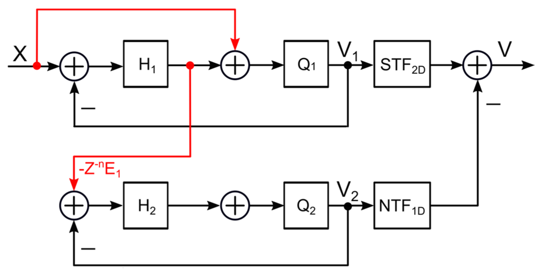
2.1. Overview of MASH and SMASH DSMs
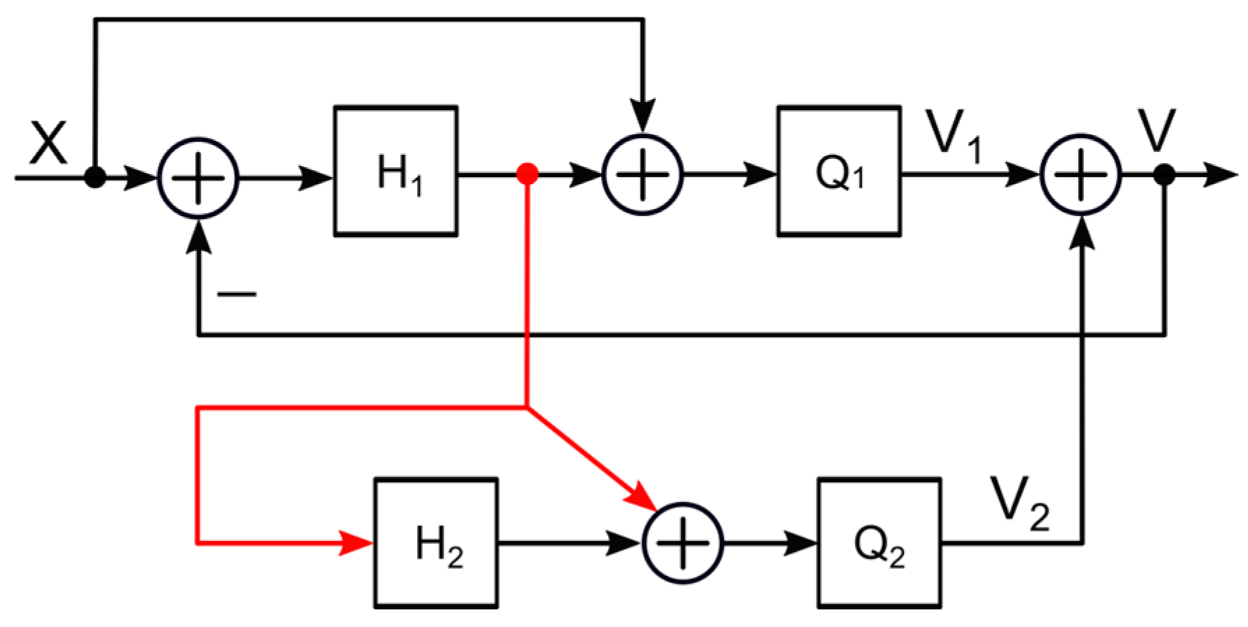
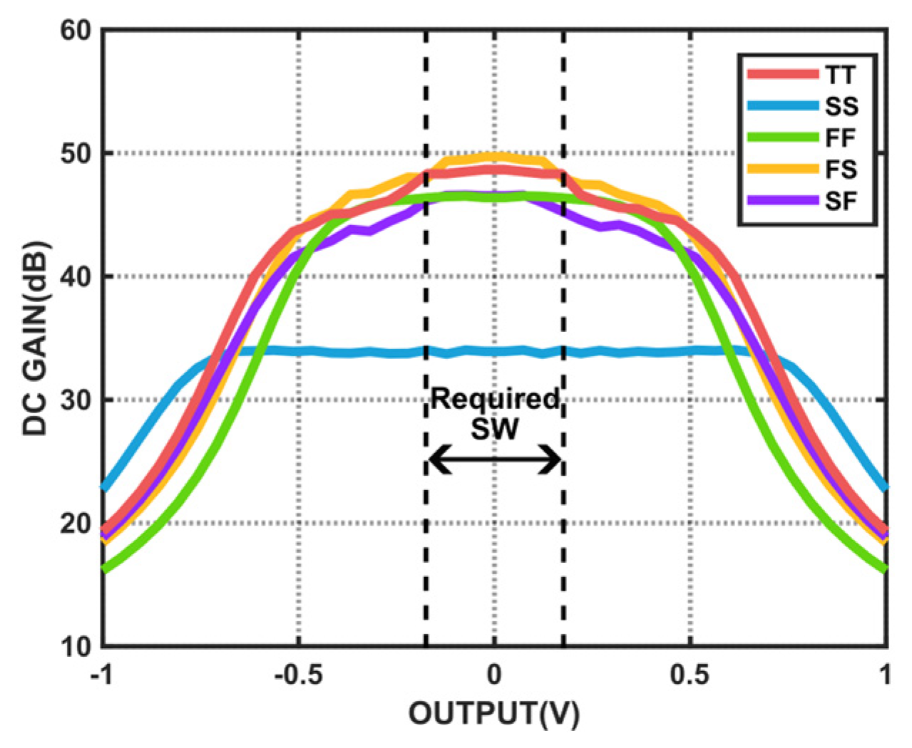
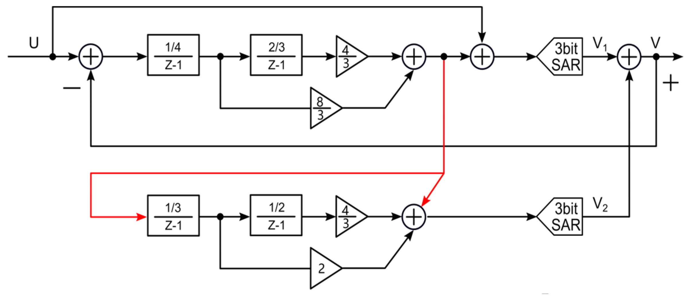
For sub-MHz-bandwidth DSMs, a MASH topology can achieve high-order noise-shaping without stability issues. By cascading multiple stages, each with its noise-shaping transfer function, the quantization noise from each stage is shaped and suppressed in subsequent stages, effectively pushing it to higher-frequency regions. The output of MASH is as follows:
V M A S H = S T F 1 A S T F 2 D X + N T F 1 A S T F 2 D N T F 1 D S T F 2 A E 1 N T F 1 D N T F 2 A E 2
where STFi and NTFi are signal and noise transfer functions of the ith-loop, and subscripts A and D represent analog and digital transfer functions, respectively. If the first loop utilizes the low-distortion structure, the output of the H1 is −ZnE1, which is the product of the quantization noise of the 1st loop and the delay of n cycles. As a result, it can feed into the input of the second loop directly without E1 extraction DACs, as shown in Figure 1. However, these structures require high-gain amplifiers to minimize the quantization error leakage due to the mismatch between analog and digital filters. To overcome this difficulty, the SMASH topology is proposed, as shown in Figure 2a. The DC gain requirements of the amplifiers in SMASH are not as high as those in MASH. The output of the SMASH can be given as in [4,12].
V S M A S H = S T F 1 X + N T F 1 1 S T F 2 E 1 N T F 1 N T F 2 E 2
Instead of eliminating E1, the quantization noise E1 and E2 are both shaped by NTF1NTF2 if 1 − STF2 = NTF2, which releases a high DC gain requirement. If adopting the low-distortion structure in the SMASH topology, the output of the H1 is not −ZnE1 as the second stage is subtracted from the first loop and changes the NTF of the first loop. As Figure 2b shows, the output of the first loop is VH1, and it satisfies the following:
V H 1 = 1 + H 1 + H 2 + H 1 H 2 H 1 E 1 1 + H 1 1 + H 1 + H 2 + H 1 E 2 1 + H 1 + H 2
Equation (3) shows that VH1 is not a simple combination of E1 and E2. In contrast, E1 and E2 have undergone a series of polynomials. The overall output of the SMASH with low-distortion structure is as follows:
V = X + E 1 ( 1 + H 1 + H 2 + H 1 H 2 ) ( 1 + H 1 ) ( 1 + H 1 + H 2 ) E 2 1 + H 1 + H 2 = X + N T F 1 N T F 1 + N T F 2 N T F 1 N T F 2 E 1 + N T F 1 + N T F 2 N T F 1 N T F 2 N T F 1 N T F 2 E 2
It can be seen that the quantization noise E1 and E2 are not shaped by NTF1NTF2, which is contrary to the principle of SMASH. Therefore, the low-distortion structure is not applicable in a conventional SMASH.

2.2. CDL SMASH DSMs

To avoid the dedicated E1 extraction operation, the CDL SMASH is proposed in [12]. By adopting the low-distortion structure in the traditional SMASH and removing the feedback DAC in the cascaded loop, the output of the H1 can be used directly as the input to the second loop and the second-stage quantizer, as shown in Figure 3. The transfer function of V1, V2 and V here are given by
V 1 = X H 1 1 + H 1 V 2 + 1 1 + H 1 E 1
V 2 = H 1 1 + H 2 1 + 2 H 1 + H 1 H 2 E 1 + 1 + H 1 1 + 2 H 1 + H 1 H 2 E 2
V = V 1 + V 2 = X + 1 1 + 2 H 1 + H 1 H 2 ( E 1 + E 2 )
From Equations (5)–(7), H1 = H2 = H is necessary for the polynomial 1 + 2H1 + H1H2 to be merged into (1 + H)2. Therefore, the quantization noise can be shaped without causing any stability problems, and the resulting output V can be written as follows [12]:
V = X + 1 1 + H 2 E 1 + E 2
To ensure the system’s stability, the coefficient of the two loops must be equal. However, the resistor R and capacitor C in CT DSM are susceptible, and the degree of variation differs. The capacitor ratio determines the coefficients in the DT DSM, while the coefficients of the CT DSM depend on the resistor–capacitor product [13]. Consequently, DT ADC outperforms CT ADC in terms of PVT stability. As a result, this paper adopts the DT operation to obtain superior PVT stability.
After a closer look, the principle of the CDL SMASH is similar to that of a Zoom ADC. The Zoom ADC combines the advantages of the SAR and DSM that can achieve high DR and high resolution [14,15,16,17]. The input signal is sent into the SAR ADC to obtain a coarse conversion at the first, and the references of the follower ΔΣ ADC are adapted by the result of the SAR. As a result, the requirement of ΔΣ ADC is relaxed as it just needs to deal with the residue of the SAR. The first stage of the SMASH can also be regarded as coarse conversion; then, the quantization noise E1 is processed by the second loop, which is equivalent to the fine DSM of the Zoom. Finally, the output of the second loop V2 and the first loop output V1 are combined to obtain the total output V, which can be modeled as the combination of the Zoom. The comparison between the Zoom ADCs and the adopted SMASH architecture is shown in Figure 4. Zoom ADC’s demand for the gain of the amplifier is higher than that of SMASH. The SQNRmax of the 3-bit 4th-order ZOOM is 10 dB lower than 3 bit 2 + 2 CDL SMASH. The 3-bit 2 + 2 CDL SMASH only requires a 30 dB DC gain to achieve 110 dB SQNR, while the 3-bit 4th-order Zoom structure needs more than 40 dB DC gain to obtain the maximum SQNR, which is still less than that of SMASH. As a result, the adopted 2 + 2 CDL SMASH performs better than the same-order Zoom ADC in both quantization noise suppression and the gain requirements of the amplifiers.

3. Circuit Implementation

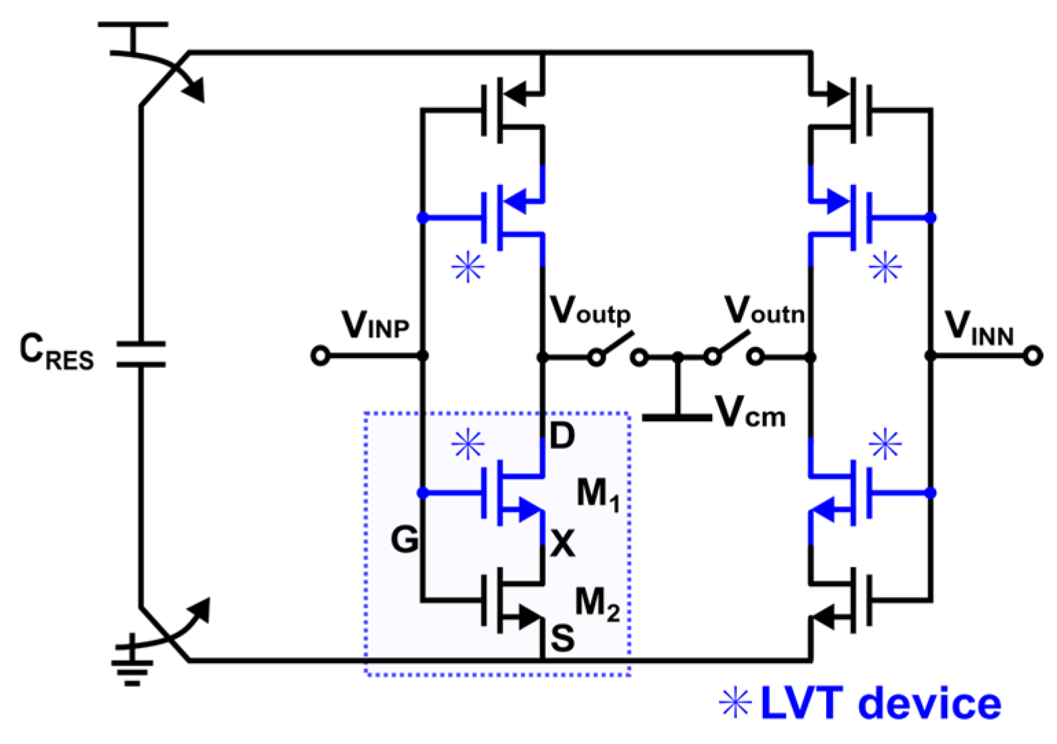
3.1. The Proposed Self-Cascoded FIA

FIAs have been widely used in ADCs for their high energy-efficiency owing to their current-reusing nature and lack of static consumption; however, they only have a limited DC gain of around 30 dB at the operating frequency of 10 MHz. In this work, the DC gain of the 1st integrator of 2 + 2 DT SMASH is required to be more than 40 dB, and the swing has to achieve 180 mV to realize the maximum SQNR. To increase DC gain, multi-stage FIAs that cascade two or more single-stage FIAs are proposed in [8,9]. Unfortunately, the input-referred in-band noise is amplified by a product of Gm2Ro1, where Gm2 is the conductance of the second stage, and Ro1 is the output resistance of the first stage. Also, cascading induces stability issue, which leads to design difficulties.
This work adopts a self-cascoded FIA to achieve the required DC gain. The schematic is shown in Figure 5. The gates of the cascoded transistors are connected to the input, avoiding the additional dedicated bias circuits and extra power. The following cascode transistors must be low-voltage threshold (LVT) devices that ensure both main input pairs function properly. As shown in Figure 5, the drain and source voltage of the M1 and M2 should satisfy the following:
V G V S V TH 1 > 0
V G V X V TH 2 > 0
One can rewrite Equation (10) as
V G V TH 2 V S > V X V S
If VTH1 = VTH2, one obtains
V G V TH 1 V S = V DSAT 1 > V X V S = V DS 1
Thus, the transistor M1 is in the linear region. Therefore, LVT devices are adopted as the cascode transistors to make the input transistors work in the saturation region. In this way, the proposed structure acts like an ordinary cascode FIA, providing large DC gain.
Figure 6 shows that the simulated DC gain of the self-cascoded FIA is beyond 45 dB and the −3 dB output swing is about 310 mV under a typical NMOS and typical PMOS (TT) corner. The DC gain is sufficient for the SMASH system under different corners even for slow NMOS and slow PMOS (SS) corners. Owing to the higher threshold voltage, the transistors are almost off at the SS corner, the self-cascoded FIA’s DC gain decreases drastically. Though a DC gain of greater than 30 dB is still enough, this can be alleviated by using a larger reservoir capacitor (CRES) in exchange with larger area and power consumption. Since the amplifiers largely determine the performance of the modulator. The amplifier’s robustness against temperature variations is also significant. Figure 7 shows the simulated DC gain versus temperature. It shows that a DC gain of 30 db can be assured except for SS corner under 0 °C, as low temperature makes the threshold voltages of the transistors even higher.

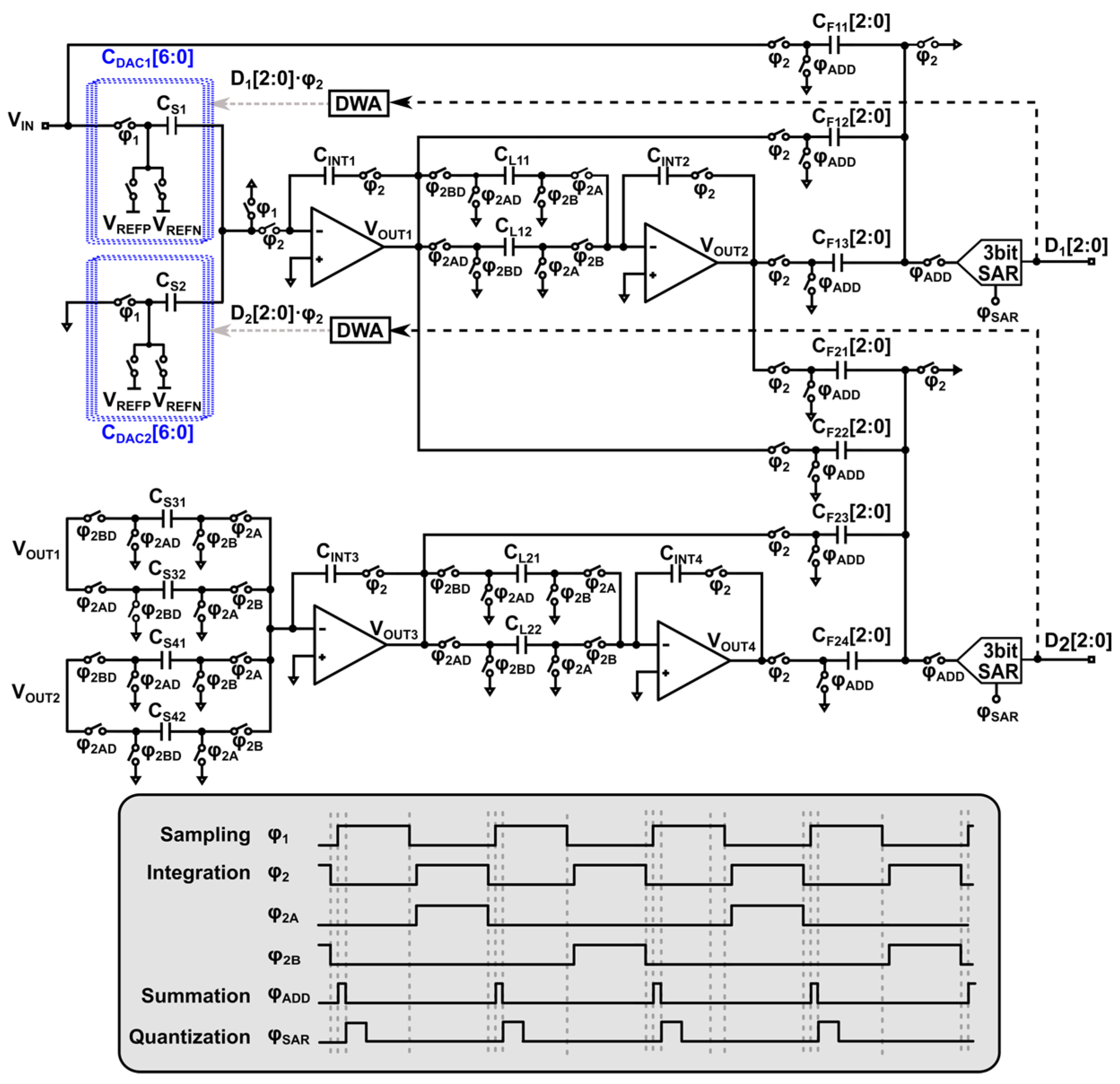
3.2. 2+2 DT SMASH DSM Implementation

Figure 8 shows a system-level block diagram of the DT DSM comprising two asynchronous SAR ADCs and two second-order loop filters. The first loop utilizes the low-distortion structure to circumvent the extraction of quantization noise E1 and the DAC of the second loop is removed, as introduced in CDL SMASH. Finally, the outputs of the two second-order loops are summed directly to generate the total output V, which, therefore, realizes fourth-order noise-shaping.
The circuit implementation (single-ended version) and timing diagram of the DT SMASH are shown in Figure 9. The first and second integrators are realized with the proposed self-cascoded FIA. The other integrators are conventional FIA because of the relaxed DC gain requirement of the second stage. This also explains the coarse–fine operation of this modulator. The quantizer of each loop is a 3-bit SAR ADC, further improving the MSA and reducing the internal swing of the loop filter.
Generally, in multi-loop DT DSMs, the passive adders and SAR quantizers occupy a part of the time to finish quantization, sacrificing the integration time of the amplifier. As a result, this places great demand on the settling capability of the amplifiers, which increases power consumption. In this work, all integrators except the first integrator work in a ping–pong method, which is realized by simultaneous sampling (integration) during φ2A2B). The duty cycles of φ2A and φ2B that are the binary frequencies of φ2 are one quarter of the value. The quantizers finish the quantization within φ1, and all the integrators start working during the integration phase φ2. Taking the second stage as an example, the two sampling capacitors function in a ping–pong way. The output voltage of the first stage Vout1 is stored in CL11 during φ2BD initially. Then, the charge would be saved in CL12 instead during φ2AD when entering the next cycle, and the charge stored in CL11 is transformed to CINT2 at the same time.
According to the coefficients of the NTF and the thermal noise requirement, the sampling and integrating capacitance are designed as CS1 = 2.5 pF. The sampling capacitors are also reused as feedback capacitors, consisting of seven-unit-element capacitors in parallel. To mitigate the mismatch of the CDACs, two DWAs are performed. CF1 samples the input as the feedforward branch, which is also implemented as the capacitor array of the first SAR quantizer. The passive capacitive adders are used to avoid a dedicated power-hungry amplifier.

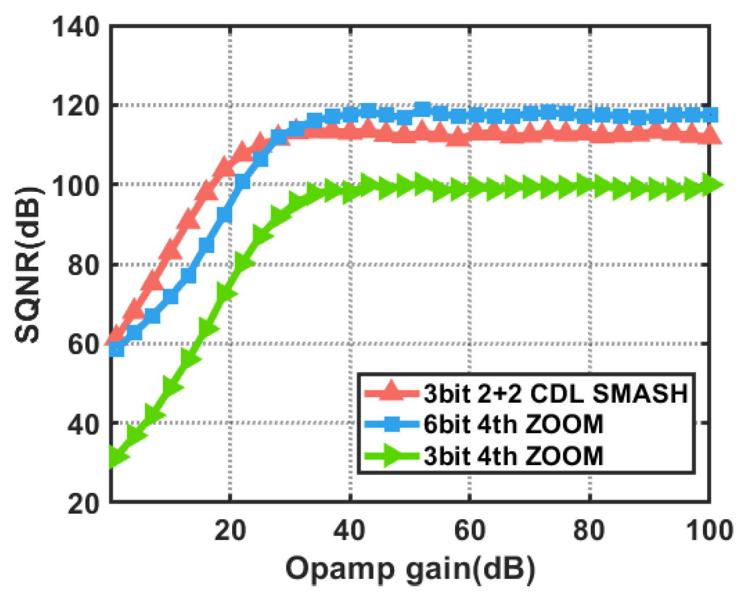
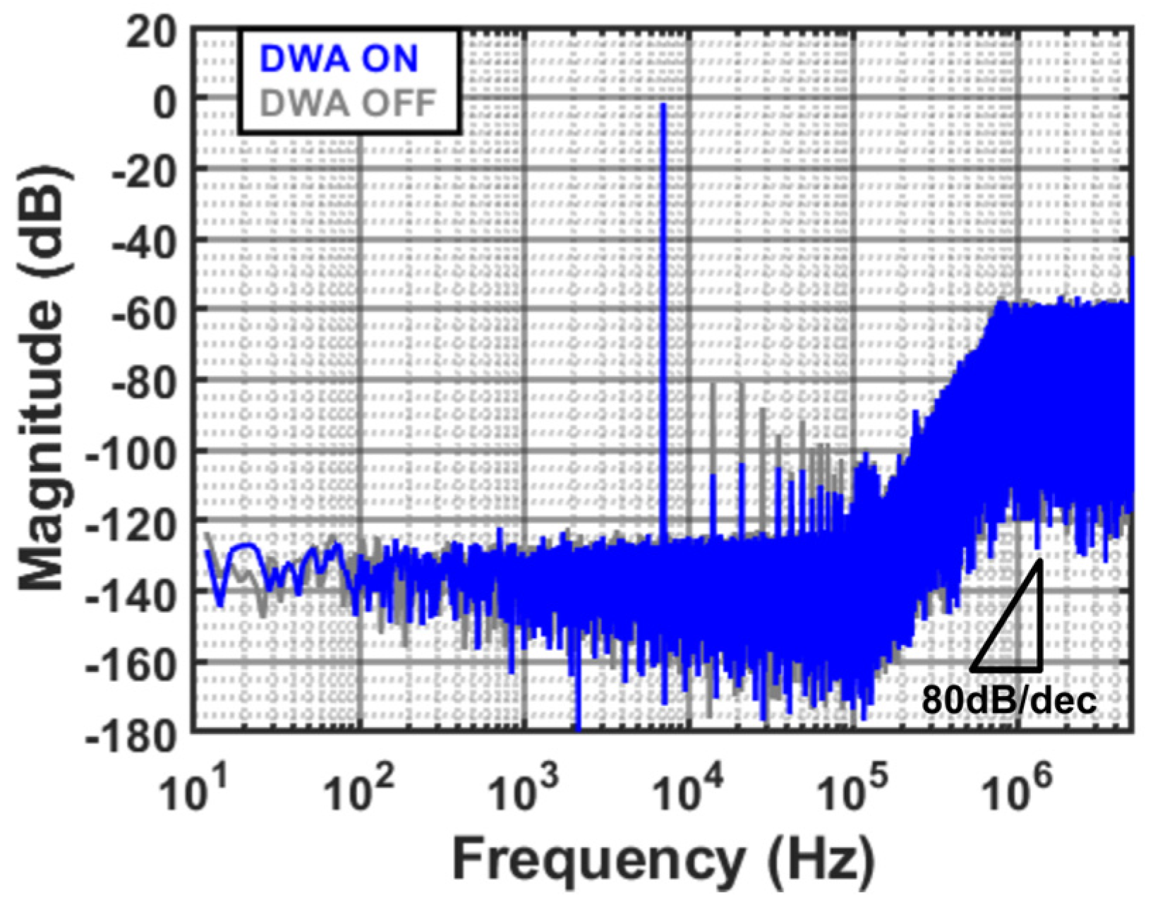
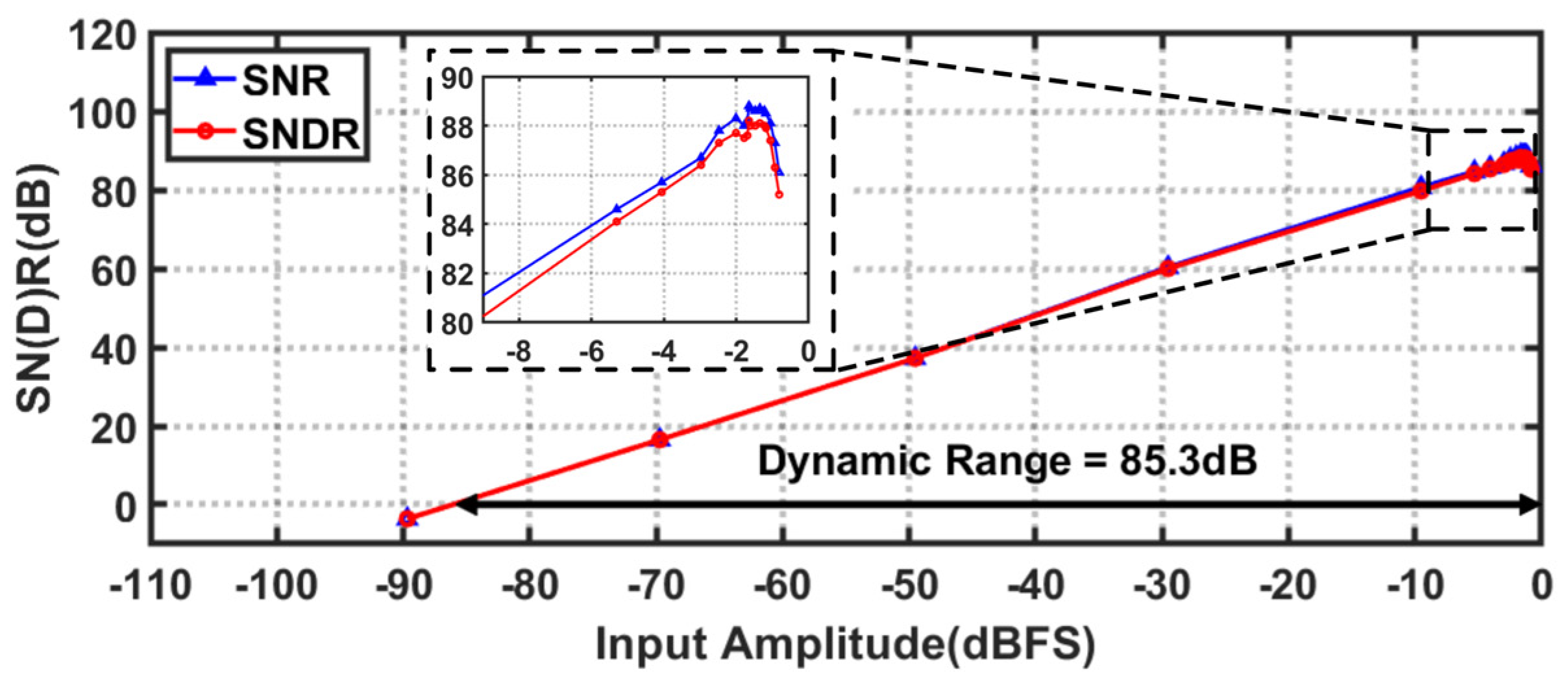
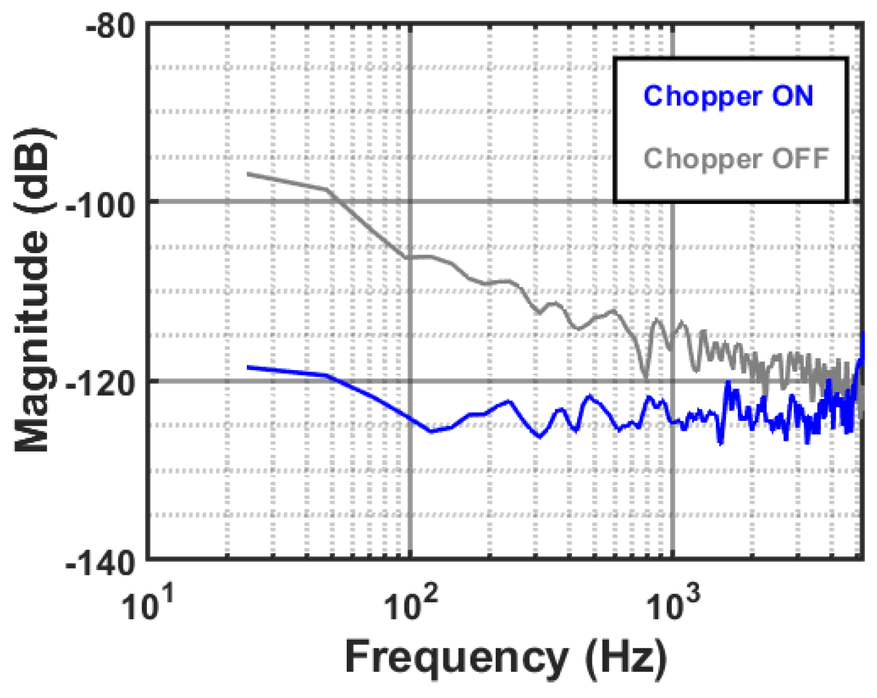
4. Measurement Results

The prototype is fabricated using a 55 nm CMOS process. Figure 10 shows the chip photo of the designed DT SMASH DSM with an active area of 0.66 mm2.
Figure 11 plots a 222-points output spectrum with a 7.2 kHz and −1.4 dBFS input signal. With a sampling frequency of 10 MHz and an OSR of 50, the prototype with DWA OFF achieves an SNDR, SNR, and SFDR of 75.3 dB, 86.9 dB, and 79.2 dB in a signal bandwidth of 100 kHz. The large harmonics are mainly limited by the mismatch between the unit elements of the feedback capacitor. These can be improved to 88.0 dB, 88.6 dB, and 102.2 dB, respectively, with DWA ON.
Figure 12 shows the measured SNR and SNDR as a function of the input amplitude, and the measured dynamic range (DR) is 85.3 dB. As the technology node shrinks, placing more circuits in the digital domain results in better efficiency. Therefore, apart from the four FIAs and the comparators in SAR ADCs, the other circuits are implemented in the digital domain. In this design, as shown in Figure 13, the overall power consumption is 249.1 μW at a supply voltage of 1.2 V and an operating clock speed of 10 MHz, from which 192.24 μW is for the analog part, 36.41 μW is for the reference, and 20.42 μW is for the digital circuitry. The corresponding SNDR-based Schreier figure-of-merit (FoMs) is 174.0 dB.
The low-frequency output spectrum is illustrated in Figure 14. It can be seen that without chopping, the modulator is dominated by the intrinsic 1/f noise of the first amplifier, while the noise of the subsequent stage is suppressed. The flicker noise can be removed by chopping, achieving a 1/f noise corner frequency of less than 50 Hz.
The measured SNDR of the three different chips across different analog supply voltage AVDDs is shown in Figure 15. The proposed modulator can work properly with ±5% supply variation with SNDR variations of less than 3 dB. When the supply voltage is below 1.12 V, the SNDR of the two chips drops sharply because the self-cascoded FIA does not work properly at such a low supply voltage, which is similar with the ss corner.
Table 2 summarizes the performance and compares it with state-of-the-art DSMs with similar bandwidths. It shows the advantage of the CDL SMASH topology and the proposed self-cascoded FIA in improving energy efficiency. The proposed ADC is a compact and energy-efficient solution for audio and sensor applications that require high resolution at a sub-MHz bandwidth. Compared to the work in [18] with similar energy efficiency, this work avoids the use of sophisticated linearization techniques and is more capable of achieving high resolution because of high-order noise shaping. On the other hand, the implementation of a large CRES occupies a considerable area.

5. Conclusions

This paper presents a sub-MHz BW DT SMASH DSM for smart sensor systems. The CDL SMASH architecture is adopted for its simplified design as well as the other advantages of using the SMASH structure. The first loop of the SMASH utilizes a low-distortion structure to avoid the extraction of quantization noise E1. The DAC of the second loop is removed, significantly reducing the area budget. Compared with the traditional MASH, the SMASH has lower requirements for the DC gain of amplifiers. Meanwhile, FIA is an energy-efficient amplifier which does not need extra bias circuits. However, a single-stage FIA can only obtain a modest DC gain of about 30 dB at an operating frequency of 10 M; therefore, this work applies a self-cascoded FIA to obtain a higher DC gain in exchange for the reduced output swing. Moreover, chopping is adopted to remove the 1/f noise without any artifacts. This prototype is fabricated and tested. The measured Schreier FoM of 174.0 dB is competitive compared to that of other state-of-the-art ADCs with similar bandwidths. In conclusion, we presented a highly energy-efficient, robust, and high-performance DT DSM. Furthermore, this work shows the potential of exploring PVT-robust gain-boosting techniques and advanced system architectures in ADC designs.

Author Contributions

Conceptualization, X.H. and Y.Y.; methodology, X.Y. and M.Z.; validation, X.H., Z.L. and S.S.; investigation, Y.Y. and J.P.; writing—original draft preparation, X.H. and Z.L.; writing—review and editing, X.H., Y.Y., J.P., Z.L., S.S., X.Y. and M.Z.; supervision, X.Y. and M.Z.; project administration, J.P. All authors have read and agreed to the published version of the manuscript.

Funding

This research is supported by the Joint R&D Fund of Beijing Smartchip Microelectronics Technology Company Limited.

Data Availability Statement

Data are contained within the article.

Conflicts of Interest

Author Yidong Yuan and Jie Pan were employed by Beijing Smartchip Microelectronics Technology Company Limited. The remaining authors declare that the research was conducted in the absence of any commercial or financial relationships that could be construed as a potential conflict of interest.

References

  1. Schreier, R.; Temes, G.C. Understanding Delta Sigma Data Converters; IEEE Press: New York, NY, USA, 2005. [Google Scholar]
  2. Kwak, Y.-S.; Cho, K.-I.; Kim, H.-J.; Lee, S.-H.; Ahn, G.-C. A 72.9-dB SNDR 20-MHz BW 2-2 Discrete-Time Resolution-Enhanced Sturdy MASH Delta–Sigma Modulator Using Source-Follower-Based Integrators. IEEE J. Solid-State Circuits 2018, 53, 2772–2782. [Google Scholar] [CrossRef]
  3. Bos, L.; Vandersteen, G.; Rombouts, P.; Geis, A.; Morgado, A.; Rolain, Y.; Van der Plas, G. Multirate Cascaded Discrete-Time Low-Pass ΔΣ Modulator for GSM/Bluetooth/UMTS. IEEE J. Solid-State Circuits 2010, 45, 1198–1208. [Google Scholar] [CrossRef]
  4. Maghari, N.; Kwon, S.; Moon, U.-K. 74 dB SNDR Multi-Loop Sturdy-MASH Delta-Sigma Modulator Using 35 dB Open-Loop Opamp Gain. IEEE J. Solid-State Circuits 2009, 44, 2212–2221. [Google Scholar] [CrossRef]
  5. Yoon, D.-Y.; Ho, S.; Lee, H.-S. A Continuous-Time Sturdy-MASH ΔΣ Modulator in 28 nm CMOS. IEEE J. Solid-State Circuits 2015, 50, 2880–2890. [Google Scholar] [CrossRef]
  6. Park, B.; Han, C.; Maghari, N. Correlated Dual-Loop Sturdy MASH CT ΔΣ ADC with Indirect Signal Feedforward. In Proceedings of the 2021 IEEE Asian Solid-State Circuits Conference (A-SSCC), Busan, Republic of Korea, 7–10 November 2021. [Google Scholar]
  7. Breems, L.J. A cascaded continuous-time Sigma Delta modulator with 67dB dynamic range in 10MHz bandwidth. In Proceedings of the 2004 IEEE International Solid-State Circuits Conference (ISSCC), San Francisco, CA, USA, 15–19 February 2004. [Google Scholar]
  8. Tang, X.; Yang, X.; Zhao, W.; Hsu, C.; Liu, J.; Shen, L.; Mukherjee, A.; Shi, W.; Li, S.; Pan, D.Z.; et al. A 13.5-ENOB, 107-μW Noise-Shaping SAR ADC With PVT-Robust Closed-Loop Dynamic Amplifier. IEEE J. Solid-State Circuits 2020, 55, 3248–3259. [Google Scholar] [CrossRef]
  9. Tang, X.; Yang, X.; Liu, J.; Wang, Z.; Shi, W.; Pan, D.Z.; Sun, N. A Bandwidth-Adaptive Pipelined SAR ADC with Three-Stage Cascoded Floating Inverter Amplifier. IEEE J. Solid-State Circuits 2023, 58, 2564–2574. [Google Scholar] [CrossRef]
  10. Meng, L.; Chen, J.; Zhao, M.; Tan, Z. A 1.2-V 2.87-μ W 94.0-dB SNDR Discrete-Time 2–0 MASH Delta-Sigma ADC. IEEE J. Solid-State Circuits 2023, 58, 1636–1645. [Google Scholar] [CrossRef]
  11. Kumar, R.S.A.; Krishnapura, N.; Banerjee, P. Analysis and Design of a Discrete-Time Delta-Sigma Modulator Using a Cascoded Floating-Inverter-Based Dynamic Amplifier. IEEE J. Solid-State Circuits 2022, 57, 3384–3395. [Google Scholar] [CrossRef]
  12. Park, B.; Han, C.; Maghari, N. Correlated Dual-Loop Sturdy MASH Continuous-Time Delta-Sigma Modulators. IEEE J. Solid-State Circuits 2022, 57, 2934–2943. [Google Scholar] [CrossRef]
  13. Qin, X.; Zhang, J.; Qi, L.; Sin, S.-W.; Martins, R.P.; Wang, G. Discrete-Time MASH Delta-Sigma Modulator with Second-Order Digital Noise Coupling for Wideband High-Resolution Applications. In Proceedings of the 2021 IEEE International Symposium on Circuits and Systems (ISCAS), Daegu, Republic of Korea, 23–26 May 2021. [Google Scholar]
  14. Gönen, B.; Sebastiano, F.; Quan, R.; van Veldhoven, R.; Makinwa, K.A.A. A Dynamic Zoom ADC with 109-dB DR for Audio Applications. IEEE J. Solid-State Circuits 2017, 52, 1542–1550. [Google Scholar] [CrossRef]
  15. Eland, E.; Karmakar, S.; Gönen, B.; van Veldhoven, R.; Makinwa, K.A.A. A 440-μW, 109.8-dB DR, 106.5-dB SNDR Discrete-Time Zoom ADC with a 20-kHz BW. IEEE J. Solid-State Circuits 2021, 56, 1207–1215. [Google Scholar] [CrossRef]
  16. Gönen, B.; Karmakar, S.; van Veldhoven, R.; Makinwa, K.A.A. A Continuous-Time Zoom ADC for Low-Power Audio Applications. IEEE J. Solid-State Circuits 2020, 55, 1023–1031. [Google Scholar] [CrossRef]
  17. Karmakar, S.; Gönen, B.; Sebastiano, F.; van Veldhoven, R.; Makinwa, K.A.A. A 280μW Dynamic Zoom ADC with 120 dB DR and 118 dB SNDR in 1 kHz BW. IEEE J. Solid-State Circuits 2018, 53, 3497–3507. [Google Scholar] [CrossRef]
  18. Li, H.; Shen, Y.; Cantatore, E.; Harpe, P. A 77.3-dB SNDR 62.5-kHz Bandwidth Continuous-Time Noise-Shaping SAR ADC with Duty-Cycled Gm-C Integrator. IEEE J. Solid-State Circuits 2023, 58, 939–948. [Google Scholar] [CrossRef]
  19. Vogelmann, P.; Haas, M.; Ortmanns, M. A 1.1mW 200kS/s incremental ΔΣ ADC with a DR of 91.5dB using integrator slicing for dynamic power reduction. In Proceedings of the 2018 IEEE International Solid-State Circuits Conference (ISSCC), San Francisco, CA, USA, 11–15 February 2018. [Google Scholar]
  20. Katayama, T.; Miyashita, S.; Sobue, K.; Hamashita, K. A 1.25MS/S Two-Step Incremental ADC with 100DB DR and 110DB SFDR. In Proceedings of the 2018 IEEE Symposium on VLSI Circuits, Honolulu, HI, USA, 18–22 June 2018. [Google Scholar]
  21. Theertham, R.; Koottala, P.; Billa, S.; Pavan, S. A 24mW Chopped CTDSM Achieving 103.5dB SNDR and 107.5dB DR in a 250kHz Bandwidth. In Proceedings of the 2019 Symposium on VLSI Circuits, Kyoto, Japan, 9–14 June 2019. [Google Scholar]
Figure 1. Block diagram of MASH structure with low-distortion input feedforward design.
Electronics 13 03865 g001
Figure 2. Block diagram of SMASH structure. (a) Traditional. (b) Low distortion.
Electronics 13 03865 g002
Figure 3. Block diagram of the CDL SMASH.
Electronics 13 03865 g003
Figure 4. SQNR versus amplifier gain of 3-bit SMASH, 3-bit Zoom and 6-bit Zoom.
Electronics 13 03865 g004
Figure 5. Proposed self-cascoded FIA.
Electronics 13 03865 g005
Figure 6. DC gain versus output swing of the proposed self-cascoded FIA under different corners.
Electronics 13 03865 g006
Figure 7. DC gain versus temperature variations under different corners.
Electronics 13 03865 g007
Figure 8. System level block diagram of the 2 + 2 DT SMASH with integrator coefficients.
Electronics 13 03865 g008
Figure 9. Simplified circuit diagram of the 2 + 2 DT SMASH and its timing diagram.
Electronics 13 03865 g009
Figure 10. Die photograph.
Electronics 13 03865 g010
Figure 11. Measured output spectrum with DWA on (blue) and off (gray).
Electronics 13 03865 g011
Figure 12. Measured SNR and SNDR versus input amplitude.
Electronics 13 03865 g012
Figure 13. Measured power consumption.
Electronics 13 03865 g013
Figure 14. Measured output spectrum with and without chopping.
Electronics 13 03865 g014
Figure 15. Measured SNDR versus analog supply voltage AVDD (3 chips).
Electronics 13 03865 g015
Table 1. Summary of different topologies.
TopologyExtractionResolutionNum. of DACsLoop Filter Req.Gain Req.
MASHDT 2-2No High2 High High
SMASHCT 3-1 [5]Yes  High3  Low Low 
CT 2-2 [6]No Medium2 High Low
DT 2-2 [4]Yes Medium3 Low Low
ProposedDT CDL 2-2No Medium2 Low Low
Table 2. Performance summary and comparison with state-of-the-art works.
[19][20][21][18][2]This Work
ArchitectureIncre-
mental
Incre-
mental
CTDSMCT
NSSAR
DT
SMASH
DT
SMASH
Shaping order3-4144
Technology [nm]180180180656555
Chip area [mm2]0.3630.7162.850.030.340.66
Supply [V]331.811.21.2
Bandwidth [kHz]10062525062.520,000100
OSR1504464161250
SNDR [dB]86.696.6103.577.372.988.0  ***
* ENOB [bit]14.115.816.912.511.814.3
Power [μW]1098277024,00013.520,400249.1
** FoMS [dB]171.1173.6173.7174.0162.8174.0
* ENOB = (SNDR − 1.76)/6.02; ** FoMS = SNDR + 10log10(Bandwidth/Power); *** 84–91 dB over process variation and temperature −25–80 °C. The bold in the table highlights the results of this work.
Disclaimer/Publisher’s Note: The statements, opinions and data contained in all publications are solely those of the individual author(s) and contributor(s) and not of MDPI and/or the editor(s). MDPI and/or the editor(s) disclaim responsibility for any injury to people or property resulting from any ideas, methods, instructions or products referred to in the content.

