1. Introduction
Principal Component Analysis (PCA) is a widely-used method for reducing dimensionality. It extracts from a set of observations the Principal Components (PCs) that correspond to the maximum variations in the data. By projecting the data on an orthogonal basis of vectors corresponding to the first few PCs obtained with the analysis and removing the other PCs, the data dimensions can be reduced without a significant loss of information. Therefore, PCA can be used in various applications when there is redundant information in the data. For example, in Microwave Imaging (MI), PCA is useful before image reconstruction to reduce data dimensions in microwave measurements [
1,
2,
3]. In a recent work [
4], PCA is used as a feature extraction step prior to tumor classification in MI-based breast cancer detection.
PCA involves various computing steps consisting of complex arithmetic operations, which result in a high computational cost and so a high execution time when implementing PCA in software. To tackle this problem, hardware acceleration is often used as an effective solution that helps reduce the total execution time and enhance the overall performance of PCA.
The main computing steps of PCA, which will be described thoroughly in the next section, include the computation of an often large covariance matrix, which stresses the I/O of hardware systems, and the computation of the singular values of the matrix. Since the covariance matrix is symmetric, the singular values are also the eigenvalues and can be computed either with Eigenvalue Decomposition (EVD) or with Singular Value Decomposition (SVD): the more appropriate algorithm to implement in hardware is chosen depending on the application and the performance requirements. Other important steps in PCA are the data normalization, which requires to compute the data mean, and the projection of the data on the selected PCs.
In recent years, numerous hardware accelerators have been proposed that implement either PCA in its entirety or some of its building blocks. For example, in [
5] different hardware implementations of EVD were compared and analyzed on CPU, GPU, and Field-Programmable Gate Arrays (FPGA), and it was shown that FPGA implementations offer the best computational performance, while the GPU ones require less design effort. A new FPGA architecture for EVD computation of polynomial matrices was presented in [
6], in which the authors show how the Xilinx System Generator tool can be used to increase the design efficiency compared to traditional RTL manual coding. Leveraging a higher abstraction level to improve the design efficiency is also our goal, which we pursue using the High-Level Synthesis (HLS) design approach, as we discuss later, as opposed to VHDL- or Verilog-based RTL coding. Wang and Zambreno [
7] introduce a floating-point FPGA design of SVD based on the Hestenes-Jacobi algorithm. Other hardware accelerators for EVD and SVD were proposed in [
8,
9,
10,
11].
In [
12] an embedded hardware was designed in FPGA using VHDL for the computation of Mean and Covariance matrices as two components of PCA. Fernandez et al. [
13] presented a manual RTL design of PCA for Hyperspectral Imaging (HI) in a Virtex7 FPGA. The Covariance and Mean computations could not be implemented in hardware due to the high resource utilization. Das et al. [
14] designed an FPGA implementation of PCA in a network intrusion detection system, in which the training phase (i.e., computing the PCs) was done offline and only the mapping phase (i.e., the projection of the data on the PC base) in the online section was accelerated in hardware. Our goal is instead to provide a complete PCA implementation, which can be easily adapted to the available FPGA resources thanks to the design flexibility enabled by the HLS approach.
Recently, some FPGA accelerators have been introduced that managed to implement a complete PCA algorithm. In [
15] such an accelerator was designed in a Virtex7 FPGA using VHDL, but it is applicable only to relatively small matrix dimensions. Two block memories were used for the internal matrix multiplication to store the rows and columns of the matrices involved in the multiplication, which resulted in a high resource usage. Thanks to our design approach, instead, we are able to implement a complete PCA accelerator for large matrices even with few FPGA resources.
FPGAs are not the only possible target for PCA acceleration. In [
16], all the PCA components were implemented on two different hardware platforms, a GPU and a Massively Parallel Processing Array (MPPA). Hyperspectral images with different dimensions were used as test inputs to evaluate the hardware performance. It is well known, however, that these kinds of hardware accelerators are not as energy-efficient as FPGAs. Therefore we do not consider them, especially because our target computing devices are embedded systems in which FPGAs can provide an efficient way for hardware acceleration.
To design a hardware accelerator in FPGA, the traditional approach uses Hardware Description Languages (HDL) like VHDL or Verilog. Although this approach is still the predominant design methodology, it increases the development time and the design effort. As embedded systems are becoming more complex, designing an efficient hardware in RTL requires significant effort, which makes it difficult to find the best hardware architecture. An alternative solution that is becoming more popular in recent years is the High Level Synthesis (HLS) approach. HLS raises the design abstraction level by using software programming languages like C or C++. Through the processes of scheduling, binding, and allocation, HLS converts a software code into its corresponding RTL description. The main advantage of HLS over HDL is that it enables designers to explore the design space more quickly, thus reducing the total development time with a quality of results comparable and often better than RTL design. Another important advantage is the flexibility, which we use in this work and which allows designers to use a single HLS code for different hardware targets with different resource and performance constraints.
Recently, HLS-based accelerators have been proposed for PCA. In [
17], a design based on HLS was introduced for a gas identification system and implemented on a Zynq SoC. Schellhorn et al., presented in [
18] another PCA implementation on FPGA using HLS for the application of spectral image analysis, in which the EVD part could not be implemented in hardware due to the limited resources. In [
19], we presented an FPGA accelerator by using HLS to design the SVD and projection building blocks of PCA. Although it could be used for relatively large matrix dimensions, the other resource-demanding building blocks (especially covariance computation) were not included in that design. In a preliminary version of this work [
20], we proposed another HLS-based PCA accelerator to be used with flexible data dimensions and precision, but limited in terms of hardware target to a low-cost Zynq SoC and without the support for block-streaming needed to handle large data matrices and covariance matrices, which instead we show in this paper.
The PCA hardware accelerators proposed in the literature have some drawbacks. The manual RTL approach used to design the majority of them is one of the disadvantages, which leads to an increase in the total development time. Most of the previous works, including some of the HLS-based designs, could not implement an entire PCA algorithm including all the computational units. Other implementations could not offer a flexible and efficient design with a high computational performance that could be used for different data sizes.
In this paper we close the gap in the state of the art and propose an efficient FPGA hardware accelerator that has the following characteristics:
The PCA algorithm is implemented in FPGA in its entirety.
It uses a new block-streaming method for the internal covariance computation.
It is flexible because it is entirely designed in HLS and can be used for different input sizes and FPGA targets.
It can easily switch between floating-point and fixed-point implementation, again thanks to the HLS approach.
It can be easily deployed on various FPGA-based boards, which we prove by targeting both a Zynq7000 and a Virtex7 in their respective development boards.
The rest of the paper is organized as follows. At first, in
Section 2 the PCA algorithm is described with the details of its processing units. We briefly describe in
Section 3 the application of PCA to Hyperspectral Imaging (HI), which we use as a test case to report our experimental results and to compare them with previously reported results. The proposed PCA hardware accelerator and the block-streaming method is presented in
Section 4 together with the HLS optimization techniques. The implementation results and the comparisons with other works are reported in
Section 5. Finally, the conclusions are drawn in
Section 6.
3. Hyperspectral Imaging
Although we are interested in the application of PCA to Microwave Imaging (MI), to the best of our knowledge there is no hardware accelerator for PCA in the literature that is specifically aimed at such application. In order to compare our proposed hardware with state-of-the-art PCA accelerators, we had to select another application for which an RTL- or HLS-based hardware design was available. Therefore, we selected the Hyperspectral Imaging (HI) application.
Hyperspectral Imaging (HI) sensors acquire digital images in several narrow spectral bands. This enables the construction of a continuous radiance spectrum for every pixel in the scene. Thus, HI data exploitation helps to remotely identify the ground materials-of-interest based on their spectral properties [
21].
HI data are organized in a matrix of size in which R is the number of pixels in the image and C is the number of spectral bands. Usually, there is redundant information in different bands that can be removed with PCA. In the following notations, we use interchangeably the terms and pixels, as well as and bands.
For MI, instead, the matrix could represent data gathered in C different frequencies in the microwave spectrum by R antennas, or a reconstructed image of the scattered electromagnetic field of R pixels also at C frequencies.
4. PCA Hardware Accelerator Design
Figure 1 shows the architecture of the PCA accelerator and its main components. Since the accelerator is developed in HLS using C++, the overall architecture correspond to a C++ function and its components correspond to subfunctions. At the highest level, there are two subfunctions named
Dispatcher and
PCA core. The Dispatcher reads the input data stored in an external DDR memory and sends them to the PCA core through the connecting FIFOs. The connection with FIFOs is also described in HLS with proper code pragmas.
The PCA core contains different processing units. The first is the Mean unit, which computes the mean vector corresponding to the mean value of each column of the input matrix. This vector is stored in an internal memory that is used by the next processing units, Cov and PU, for data centering. The Cov unit uses the new block-streaming method for computing the covariance matrix, which will be explained thoroughly in the following subsection. It reads the required data from two sets of FIFOs corresponding to diagonal and off-diagonal computation. Then the SVD unit computes the singular values of the covariance matrix, and the Sort and Select unit sorts them and retains the first components. Finally, the Projection unit reads the input data again and computes the multiplication between the centered data and the sorted and selected PCs to produce the final PCA output data, which are written back to the external DDR memory.
The computational cost of PCA depends on the input dimensions. When the main dimension from which the redundant information must be removed (columns or bands in HI) is lower than the other dimension (rows or pixels in HI), the PCA performance is mainly limited by the computation of the covariance matrix, due to the large number of multiplications and additions that are proportional to the number of pixels. Indeed, in the covariance computation all the pixels in one band must be multiplied and accumulated with the corresponding pixels in all of the bands. This is illustrated in
Figure 2 where the bands are specified by the letters
to
n and pixels are indicated by the indices 1 to N. The result of the covariance computation, which is the output of the Cov unit, is a matrix of size (
) that becomes the input of the SVD unit. In HI applications, in which it is true that
pixels ≫
bands, the covariance computation is the major limitation of the whole PCA design, hence its acceleration can drastically enhance the overall performance.
Multiple parallel streaming FIFOs are needed to match the parallelism of the accelerated Cov unit. The number of FIFOs is determined based on the input data dimensions and the maximum bandwidth of the external memory. Streaming more data at the same time through the FIFOs enables a degree of parallelism that is matched to the number of columns of the input matrix. It is important to note that all of the hardware components are described in a single HLS top-level function, which simplifies the addition of different flexibility options to the design such as variable data dimensions, block sizes, and number of FIFOs.
The complexity of the Cov unit compared to other parts raises the importance of the block-streaming method in covariance computation as this method allows using the same design for higher data dimensions or improving the efficiency in low-cost embedded systems with fewer hardware resources.
4.1. Block-Streaming for Covariance Computation
The block-streaming method is helpful whenever there is a limitation in the maximum size of input data that can be stored in an internal memory in the Cov unit. Therefore, instead of streaming the whole data one time, we stream “blocks” of data several times through the connecting FIFOs. There are two internal memories inside the Cov unit each of which can store a maximum number of bands () for each pixel. These memories are used in the diagonal and off-diagonal computations, so we call them “Diag” and “Off-diag” RAMs, respectively. The input data is partitioned into several blocks along the main dimension (bands) with a maximum dimension of (block size). Each block of data is streamed through the two sets of FIFOs located between the Dispatcher and Cov unit (Diag and Off-diag FIFOs) in a specific order, and after the partial calculation of all the elements of the covariance matrix for one pixel, the data blocks for the next pixels will be streamed and the partial results accumulated together to obtain the final covariance matrix.
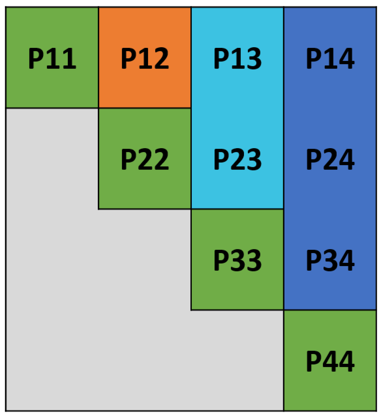
The first example is illustrated in
Figure 3 in which the total number of bands is
and the block size is
. Therefore, we have 3 blocks of data that are specified in figure as P1 to P3. The Block-streaming method consists of the following steps that can be realized from
Figure 4:
Diagonal computation:
The 3 blocks of data (P1 to P3) for the first pixel are streamed in Diag FIFOs one by one and after storage in the Diag RAM, the diagonal elements P11, P22, and P33 are computed.
Off-diagonal computation of the last block:
- (a)
Keep the last block (P3) in the Diag RAM.
- (b)
Stream the first block (P1) into Off-Diag FIFOs, store it in Off-Diag RAM, and compute .
- (c)
Stream the second block (P2) into Off-Diag FIFOs, store it in Off-Diag RAM, and compute .
Off-diagonal computation of the preceding blocks:
- (a)
Update the Diag RAM by the last values of Off-Diag RAM (P2).
- (b)
Stream the first block (P1) into Off-Diag FIFOs, store it in Off-Diag RAM, and compute .
Stream Pixels: Steps 1 to 3 are repeated for the next pixels and the results are accumulated to obtain the final covariance matrix.
The second example is illustrated in
Figure 5 in which the number of blocks is 4 and after the diagonal computation (in green color) there are 3 steps for off-diagonal computations that are indicated in 3 different colors.
Figure 6 shows the order of data storage in the Diag and Off-diag RAMs. After the 7th and 9th steps, the Diag RAM is updated by the last value of Off-Diag RAM (P3 and P2).
4.2. High Level Synthesis Optimizations
4.2.1. Tool Independent Optimization Directives and Their Hardware Implementation
To introduce the principles behind the hardware optimization techniques used in the proposed design, a more abstract description of the high-level directives is presented in this part without references to a specific hardware design tool. In
Figure 7 the most widely used optimization directives are illustrated with their corresponding hardware implementation. These directives are
Loop Pipelining, Loop Unrolling, Array Partitioning, and
Dataflow.Loop Pipelining allows multiple operations of a loop to be executed concurrently by using the same hardware iteratively. Loop Unrolling creates multiple instances of the hardware for the loop body, which allows some or all of the loop iterations to occur in parallel. By using Array Partitioning we can split an array, which is implemented in RTL by default as a single block RAM resource, into multiple smaller arrays that are mapped to multiple block RAMs. This increases the number of memory ports providing more bandwidth to access data. Finally, the Dataflow directive allows multiple functions or loops to operate concurrently. This is achieved by creating channels (FIFOs or Ping-Pong buffers) in the design, which enables the operations in a function or loop to start before the previous function or loop completes all of its operations. Dataflow directive is mainly used to improve the overall latency and throughput of the design. Latency is the time required to produce the output after receiving the input. Throughput is the rate at which the outputs are produced (or the inputs are consumed) and is measured as the reciprocal of the time difference between two consecutive outputs (or inputs).
The PCA hardware accelerator is designed in C++ using Vivado HLS, the HLS development tool for Xilinx FPGAs. The above-mentioned optimization directives can be applied easily in HLS by using their corresponding code pragmas. HLS enables us to specify the hardware interfaces as well as the level of parallelism and pipelined execution and specific hardware resource allocation thanks to the addition of code pragmas. By exploring different combinations of the optimization directives, it is possible to determine relatively easily the best configuration in terms of latency and resource usage. Therefore, several interface and hardware optimization directives have been applied in the HLS synthesis tool, as explained below.
4.2.2. Input Interfaces
The main input interface associated to the Dispatcher input and the output interface associated to the PU output consist of AXI master ports, whose number and parallelism are adapted to the FPGA target. For the Zynq of the Zedboard, four AXI ports (with a fixed width of 64 bits) are connected to the Dispatcher input in such a way to fully utilize the available memory bandwidth. In the Virtex7 of the VC709 board we can use instead only one AXI port with a much larger bit-level parallelism. The output interface for both boards is one AXI master port that is responsible for writing the output to the memory. Other interfaces are specified as internal FIFOs between the Dispatcher and the PCA core. As shown in
Figure 1, four sets of FIFOs send the streaming data (containing a data block of bands) from the Dispatcher to the corresponding processing units in the PCA core. Mean and Projection units receive two sets of FIFOs and Cov unit receives another two. Each set of FIFOs is partitioned by
, the size of a data block, so that there are
FIFOs in each set.
These FIFOs are automatically generated by applying the Vivado HLS Dataflow directive for the connection between the Dispatcher and the PCA core. This directive lets the two functions execute concurrently and their synchronization is made possible by the FIFO channels automatically inserted between them.
4.2.3. Code Description and Hardware Optimizations
In this part the code description for each PCA component is presented. To optimize the hardware of each PCA unit, we analyzed the impact of different HLS optimizations on the overall performance. Specifically, we considered the impact of loop pipelining, loop unrolling, and array partitioning on latency and resource consumption. The best HLS optimizations are selected in such a way that the overall latency is minimized by utilizing as many resources as required.
The Mean unit computes the mean values of all the pixels in each band. The code snippet for the Mean unit is presented in Algorithm 2 and consists of two loops on the rows and columns to accumulate the pixel values and another loop for the final division by the number of rows.
| Algorithm 2: Mean computation |
mean_row_loop:
for r=0 to R do
#pragma HLS PIPELINE
mean_col_loop:
for c=0 to C do
;
;
end
end
Divide_loop:
for c=0;c<C;c++ do
;
end |
The best HLS optimization for the Mean unit is to pipeline the outer loop (line #pragma HLS PIPELINE in Algorithm 2), which reduces the Initiation Interval (II), i.e., the index of performance that corresponds to the minimum time interval (in clock cycles) between two consecutive executions of the loop (ideally, II = 1). In addition, the memory arrays and are partitioned by (not shown in the code snippet) to have access to multiple memory locations at the same time, which is required for the loop pipelining to be effective, otherwise the II will increase due to the latency needed to access a single, non-partitioned memory.
The Cov unit uses the block-streaming method to compute the covariance matrix. Its pseudo code is presented in Algorithm 3. The HLS optimizations include loop pipelining, unrolling, and the arrays full partitioning. In Algorithm 3 full indexing is not displayed to make the code more readable and only the relation between the variables and the indexes is shown by the parentheses. For example, DiagFIFO(r,b) indicates that the indexes of variable DiagFIFO are proportional to (r,b). The standard Cov computation is adopted from [
20] and is used for diagonal covariance computations. The write function in the last line writes the diagonal and off-diagonal elements of covariance matrix from variables CovDiag and CovOff to the corresponding locations in CovOut. As shown in Algorithm 3, there are two pipeline directives that are applied to the loops on the diagonal and off-diagonal blocks, respectively. The memory arrays need to be fully partitioned, which is required to unroll the inner loops. As described before, a thorough analysis of different possible optimizations was performed to find out a trade-off between resource usage and latency.
| Algorithm 3: Cov computation, block-streaming |
for r=0 to R do /* Stream Pixels */
for b=0 to NB do /* Diagonal Computations, */
#pragma HLS PIPELINE
;
/* Start standard Cov computation [20] */
for c1=0 to do
for c2=c1 to do
…/* indexing */
;
end
end
/* Finish standard Cov computation */
end
for ct=1 to NB do /* Off-Diagonal computations */
for b=0 to NB-ct do
#pragma HLS PIPELINE
if Step3(a) then /*refer to Section 4.1, the four steps of block-streaming method*/
;
end
;
;
end
end
end
/* Write to the final Cov matrix */
; |
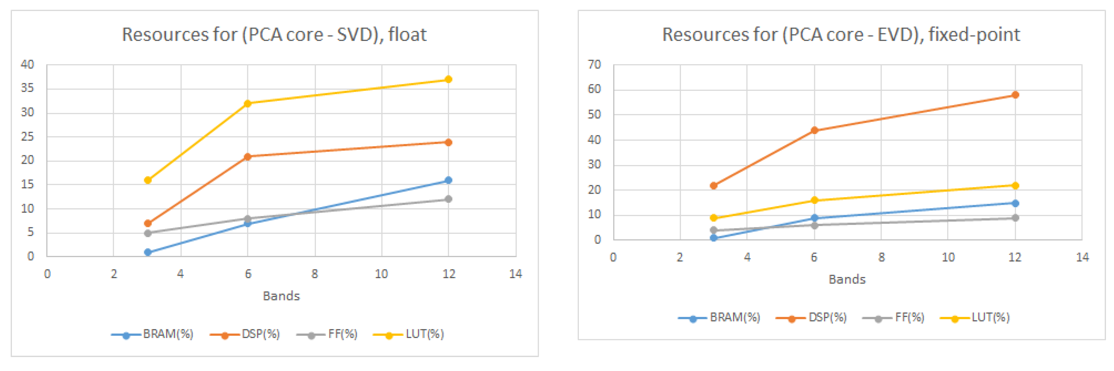
The next processing unit is the EVD of the covariance matrix. For real and symmetric matrices (like the covariance matrix) EVD is equal to SVD and both methods can be used. For SVD computation of floating-point matrices, there is a built-in function in Vivado HLS that is efficient especially for large dimensions. On the other hand, a fixed-point implementation of EVD is highly beneficial for embedded systems due to the lower resource usage (or better latency) compared to the floating-point version of the same design.
For these reasons, in this paper we propose two versions of the PCA accelerator. The first one is the floating-point version, which uses the built-in HLS function for SVD computation. The second one is the fixed-point version, which uses the general two-sided Jacobi method for EVD computation [
22,
23]. The details of this method for computing EVD is shown in Algorithm 4. As we will show in the results section, there is no need to add any HLS optimization directives to the fixed-point EVD (for our application) because the overall latency of the PCA core, which includes EVD, is lower than the data transfer time, so there is no benefit in consuming any further resources to optimize the EVD hardware. We do not report the code of the floating-point version as it uses the built-in Vivado HLS function for SVD (Vivado Design Suite User Guide: High-Level Synthesis, UG902 (v2019.1), Xilinx, San Jose, CA, 2019
https://www.xilinx.com/support/documentation/sw_manuals/xilinx2019_1/ug902-vivado-high-level-synthesis.pdf).
| Algorithm 4: EVD computation, Two-sided Jacobi method |
/*Initialize the eigenvector matrix V and the maximum iterations */
; /* I is the identity matrix */
for l=1 to do
for all pairs i<j do
/* Compute the Jacobi rotation which diagonalizes */
; ;
;;
/* update the submatrix */
;
;
;
/* update the rest of rows and columns i and j */
for k=1 to bands except i and j do
;
;
;
;
end
/* update the eigenvector matrix V /*
for k=1 to bands do
;
;
;
end
end
end |
The last processing unit is the Projection Unit (PU), which computes the multiplication between the centered data and the principal components. Algorithm 5 presents the code snippet for the PU. Similar to the Mean unit, we applied some optimizations to this code. The second loop is pipelined and, as a consequence, all the inner loops are unrolled. In addition, the memory arrays involved in the multiplication must be partitioned. For more information on the hardware optimizations for Mean and PU and their impact on the latency and resource usage please refer to [
20].
| Algorithm 5: Projection computation |
for r=0 to R do
for c1=0 to L do
#pragma HLS PIPELINE
;
for n=0 to C do
…/* Index control */
;
end
for c2=0 to C do
;
end
;
end
end |
4.3. Fixed-Point Design of the Accelerator
There are many considerations when selecting the best numerical representation (floating- or fixed- point) in digital hardware design. Floating-point arithmetic is more suited for applications requiring high accuracy and high dynamic range. Fixed-point arithmetic is more suited for low power embedded systems with higher computational speed and fewer hardware resources. In some applications, we need not only speed, but also high accuracy. To fulfill these requirements, we can use a fixed-point design with a larger bit-width. This increases the resource usage to obtain a higher accuracy, but results in a higher speed thanks to the low-latency fixed-point operations. Therefore, depending on the requirements, it is possible to select either a high-accuracy low-speed floating-point, a low-accuracy high-speed fixed-point, or a middle-accuracy high-speed fixed-point design. Available resources in the target hardware determine which design or data representation is implementable on the device. In high-accuracy high-speed applications, we can use the fixed-point design with a high resource usage (even more than the floating-point) to minimize the execution time.
To design the fixed-point version of the PCA accelerator, the computations in all of the processing units must be in fixed-point. The total Word Length (WL) and Integer Word Length (IWL) must be determined for every variable. The range of input data and the data dimensions affect the word lengths in fixed-point variables, so the fixed-point design may change depending on the data set.
For our HI data set with 12 bands, we used the MATLAB fixed-point converter to optimize the word lengths. In HLS we selected the closest word lengths to the MATLAB ones because some HLS functions do not accept all the fixed-point representations (for example in the fixed-point square root function, IWL must be lower than WL).
The performance of EVD/SVD depends only on the number of bands. As we will see in the next section, the latency of our EVD design in HLS is significantly higher than the HLS built-in SVD function for floating-point inputs. One possible countermeasure is to use the SVD as the only floating-point component in a fixed-point design to obtain better latency, by adding proper interfaces for data-type conversion. However, when the data transfer time (i.e., the Dispatcher latency) is higher than the PCA core latency, the fixed-point EVD is more efficient because of the lower resource usage, which is the case for a small number of bands.
4.4. Hardware Prototype for PCA Accelerator Assessment with the HI Data Set
The proposed hardware design is adaptable to different FPGA targets and its performance will be evaluated in the results section in particular for two test hardware devices. In this subsection, as an example of system-level implementation using our flexible accelerator we introduce its implementation on a low-cost Zynq SoC mounted on the Zedboard development board. We used this implementation to evaluate our PCA accelerator on the HI data set. The details are illustrated in
Figure 8. The input data set is stored in an SD card. The Zynq Processing System (PS) reads the input data from the SD card and writes them to the DDR3 memory. The Zynq FPGA reads the data from the DDR3 memory by using two High Performance (HP) ports (Zynq SoC devices internally provide four HP interface ports that connect the Programmable Logic (PL) to the Processing System (PS)). As the HI data consist of images in 12 bands and each pixel has an 8-bit data width, to match the processing parallelism we need an I/O parallelism of 12 × 8 = 96 bits to read all the bands at once. Therefore, we use two 64-bit HP ports for the input interface. After the PCA computation in the accelerator, the output is written back to the DDR3 memory through the first HP port by using an
AXI Smart Connect IP block (AXI smart connect IP block connects one or more AXI memory-mapped master devices to one or more memory-mapped slave devices). Finally, the Zynq PS reads the PCA outputs from the DDR3 and writes them to the SD card.
For other applications or different FPGA targets, the connection of the PCA accelerator to the I/O system or to a processor is easily adapted thanks to the flexibility enabled by the HLS approach. It is important to note that in many designs the hardware might be so fast that its performance becomes limited by the memory speed. To avoid this problem, it is necessary that the consumption rate of the hardware that fetches the data from the DDR memory is matched to the speed of that memory. In particular, in our design, by considering the maximum bandwidth (Gb/s) of the external DDR memory and the clock frequency F (GHz) of the Dispatcher unit, we can obtain the maximum bit-width as for the PCA accelerator input connected to the Dispatcher input. Depending on the input data set and the number of bands, we can obtain the maximum required I/O parallelism. For example, if the number of bands is B and the data width of each pixel is bits, we need a maximum of to read one pixel for all the bands at once in one clock cycle. The final input bit-width of the Dispatcher () is selected in such a way that we do not exceed the memory bandwidth. Therefore, if , then . Otherwise, we have to fix the Dispatcher input bit-width to (note that the Dispatcher input is an AXI port and its data width must be a power of 2 and a multiple of 8. In addition, some FPGA targets, like the Zedboard, can read data from memory using separate AXI ports (HP ports)). It should be noted that all the above-mentioned conditions can be easily described in HLS using a set of variables and C++ macros that are set at the design time. In order to map the design into a new FPGA target, the only required change is to adjust the pre-defined variables based on the hardware device.


