Article

Test Solution for Heatsinks in Power Electronics Applications

by
Davide Piumatti
1,*,
Stefano Borlo
2,
Matteo Vincenzo Quitadamo
3,
Matteo Sonza Reorda
1,
Eric Giacomo Armando
2 and
Franco Fiori
3
1
Department of Control and Computer Engineering (DAUIN), Politecnico di Torino, 10129 Turin, Italy
2
Department of Energy (DENERG), Politecnico di Torino, 10129 Turin, Italy
3
Department of Electronics and Telecommunications (DET), Politecnico di Torino, 10129 Turin, Italy
*
Author to whom correspondence should be addressed.
Electronics 2020, 9(6), 1020; https://doi.org/10.3390/electronics9061020
Submission received: 22 May 2020 / Revised: 10 June 2020 / Accepted: 17 June 2020 / Published: 19 June 2020
(This article belongs to the Section Power Electronics)

Abstract

:
Power electronics technology is widely used in several areas, such as in the railways, automotive, electric vehicles, and renewable energy sectors. Some of these applications are safety critical, e.g., in the automotive domain. The heat produced by power devices must be efficiently dissipated to allow them to work within their operational thermal limits. Moreover, numerous ageing effects are due to thermal stress, which causes mechanical issues. Therefore, the reliability of a circuit depends on its dissipation system, even if it consists of a simple passive heatsink mounted on the power device. During the Printed Circuit Board (PCB) production, an incorrect assembly of the heatsink can cause a worse heat dissipation with a significant increase of the junction temperatures (Tj). In this paper, three possible test strategies are compared for testing the correct assembling of heatsinks. The considered strategies are used at the PCB end-manufacturing. The effectiveness of the different test methods considered is assessed on a case study corresponding to a Power Supply Unit (PSU).

1. Introduction

A relevant issue in power electronics applications is the management of the thermal aspects, i.e., the dissipation of the heat produced by any power device. The high voltages and currents related to these devices may cause an unwanted increase of their junction temperatures (Tj). Many of the electrical features of the power devices depend also on the junction temperature, e.g., the drain-source resistance (Rds,on) of a Metal-Oxide-Semiconductor Field-Effect Transistor (MOSFET) depends on the Tj [1]. This involves numerous issues in terms of the power efficiency of power applications [2] and in terms of the reliability of power systems.
The increase of the junction temperature in power devices leads to numerous mechanical stresses [3] inside the device itself, which increases the probability of malfunction and breakage of the power device. The materials used in the power devices (e.g., silicon, copper, iron, oxides, plastic) have different thermal expansion coefficients. When the temperature increases, these materials have different thermal dilatation causing considerable physical stress inside the device [3]. In addition to mechanical stress, there are also numerous device ageing phenomena associated with the temperature increase [4]. Due to ageing, the electrical parameters of the devices may change, reducing their average life [5,6]. The mechanical stress and the ageing phenomena of the device are the main cause of the breakdown of power devices [7].
Several cooling strategies [8] have been introduced to dissipate the excess of heat produced by the electronic devices and to avoid an undesired temperature increase. Passive heatsinks are the most commonly adopted approach. These heatsinks are implemented with different copper or aluminum cooling fins arranged to ease the dispersion of heat by convection. Typically, a passive heatsink is considered as efficient, reliable, and inexpensive. However, it normally has a significant physical volume and a considerable weight.
As an alternative to passive heatsinks, active heatsinks can be used. By means of a fan, it is possible to force a constant airflow between the fins of the heatsink to facilitate the heat dispersion. In more complex systems, it is possible to use the same principle for forcing a constant liquid flow within the heatsink. The active heatsinks have a smaller physical volume and allow a greater dispersion of the heat produced by the power devices. However, they are ineffective if the cooling fan or of the circulation pump do not work correctly. However, the cooling systems used in power systems require adequate levels of reliability; their malfunction can cause temperature increases in power devices causing malfunction or breakage.
The main contribution of this paper is to propose a methodology for assessing the effectiveness of different test strategies used to verify the correct operation of the cooling systems. The test procedures considered have the target of checking the correct assembly of the heatsinks on the power devices, as discussed in [9,10]. A bad assembly of the heatsink propagates the heat to the surrounding environment to a lesser degree, resulting in a junction temperature rise. The test strategies considered are applied as an end-of-line stage during the production on the final Printed Circuit Board (PCB). In the final PCB, all electrical components are assembled, including the heatsinks.
The tests strategies considered are based on the in-circuit test approach and functional test approach. Moreover, a further hybrid approach realized combining the previous two strategies was considered. The hybrid approach (called observability enhanced functional test) represents an improvement of the functional test approach. The strategies were evaluated on different devices assembled on a private heatsink or sharing the same heatsink, i.e., the heatsink was assembled on the same power devices. The evaluation of the test procedures was performed using a thermal model of the dissipation system. The thermal model was used to perform a thermal simulation together with the electrical one; in other words, an electrothermal simulation of the system was performed using a circuit simulator. Some thermal faults were considered in the thermal model of the system. This paper uses the concept of thermal fault associated with an incorrect heatsink assembly [9]. In this work, some typical power devices were considered, such as Insulated Gate Bipolar Transistors (IGBTs) and power diodes.
This work shows that the effectiveness of the considered test strategies strongly depends on the circuit on which they are used; in other words, some electrical components can hide the effects of the faults during the tests. Therefore, the effectiveness of the test is inhibited. In general, the observability enhanced functional test approach is particularly effective for testing the heatsink’s assembly, as discussed in this paper. The three test strategies considered in this paper were evaluated on a real case study corresponding to a Power Supply Unit (PSU) for industrial applications.
This work extends two previous works [9,10]. In Reference [9], a test procedure applicable to MOSFET devices was discussed. In that work, the MOSFETs were mounted on a passive heatsink. In Reference [9], the effects of different thermal faults on power devices are considered and analyzed. Furthermore, in Reference [9], some possible thermal faults are experimentally reproduced in the laboratory in order to understand the real impact of the incorrect heatsink assembly on power devices. The second work [10] developed a thermal model of the heat dissipation system. The model discussed in [10] considers a single power device assembled on the heatsink. This model is useful for identifying the maximum mechanical tolerances associated with the heatsink assembly, e.g., the maximum possible distance between the device and the heatsink or the minimum contact surfaces between the device and the heatsink. For the purpose of the work reported in [10], the power device was not yet assembled on the PCB.
In the current work, the heatsink was assembled on the PCB and the effectiveness of the test procedures considered can be influenced or inhibited by the PCB circuit, as discussed in this paper.
The paper is organized in different sections; Section 2 provides the reader with some useful information on the end-of-manufacturing test and about the thermal models. Section 3 introduces the concept of thermal faults and illustrates the three test strategies considered in this paper. Section 4 presents the selected case study and the thermal model of the dissipation system used. Section 5 presents and elaborates on the experimental results obtained. Finally, Section 6 draws some conclusions.

2. Background

In this section, different concepts related to the typical end-of-manufacturing tests performed on PCBs in an industrial environment are shown. Furthermore, some aspects of the thermal models are discussed. Finally, the Temperature-Sensitive Electrical Parameters (TSEP) of the IGBT and the diode devices are discussed.

2.1. End-of-Manufacturing Tests

The purpose of this section is to provide the reader with some basic information about the main test strategies implemented at the end-of-manufacturing in an industrial environment. The purpose of these tests is to verify the correct assembly of the final PCB. As indicated in [11], 75% of manufacturing defects occur during the assembly of the PCBs, while the remaining 25% depend on electronic devices already defective before the assembly phase. The main test strategies used at the end-of-line phase are the in-circuit test and the functional test [11,12].
The in-circuit test is performed through Automatic Test Equipment (ATE); the ATE is able to directly contact some pins of any electronic devices soldered on the PCB. Different thin and precise probes of the ATE are used to contact the interest points of the circuit. The electrical contact operation can be performed in two ways, with the bed of nails [11] approach or with the flying probes [11] approach. In the first one, different needles exist in the ATE test compartment, and the board is placed over the needles to implement the electrical contacts. In the second one, a robotic arm with some needles performs the electrical contacts moving around over the PCB. In this paper, the flying probes approach was considered. The electrical contact can be performed on the welding of the component to be tested, or by a test point. As discussed in [11], a test point is a location on a PCB used to measure an electrical value or to apply a test signal. The test points are placed during the PCB design phase for facilitating the test procedures. Through the different probes positioned on the PCB, the ATE imposes some voltages or currents in the circuit and simultaneously measures different voltages or currents. In this way, some electrical stimuli are applied to the device under test to verify its correct operation after the PCB assembly phase. For example, consider a resistor; it is possible to test it by imposing a voltage (Vtest) at its pins and measuring the current (IM) that passes through the device, as shown in Figure 1. The probes are automatically moved on the component to be tested; the ATE forces the test stimuli and performs the necessary electrical measurements. Electrical measurements are processed by the ATE and the results compared to the expected ones.
The stimuli applied to the circuit can propagate in an undesired way; this phenomenon can inhibit the test or damage other devices present in the PCB. Therefore, it is often necessary to place additional guard probes [12,13,14] on the PCB. These guard probes are ground connections used for isolating the device under test; the usage of these probes is well known in the industrial field, as it is widely discussed in [13]. The guard probes can also be used for the power circuits [14].
The functional test is performed by applying some electrical stimuli to the PCB input ports and observing the PCB behavior on the PCB output ports. A functional test is performed considering only the design specifications of the PCB. The stimuli applied to the PCB are compliant with the technical specifications of the PCB defined during the design phase of the circuit. The values observed on the PCB output signals must be compliant with the PCB design specifications. If there is a fault, the measurement performed is different from the expected one. This first functional approach based only on the observation of the PCB output ports is called the base functional test. Moreover, it is possible to increase the observability of the base functional test by using the observability enhanced functional test approach [15], where ATE is used. During this test, some electrical measurements are performed in different points of the PCB resorting to some ATE probes; the measurements are performed while the PCB is functionally stimulated. The signals measured by the test equipment during the observability enhanced functional test must be compliant with the PCB design specifications.

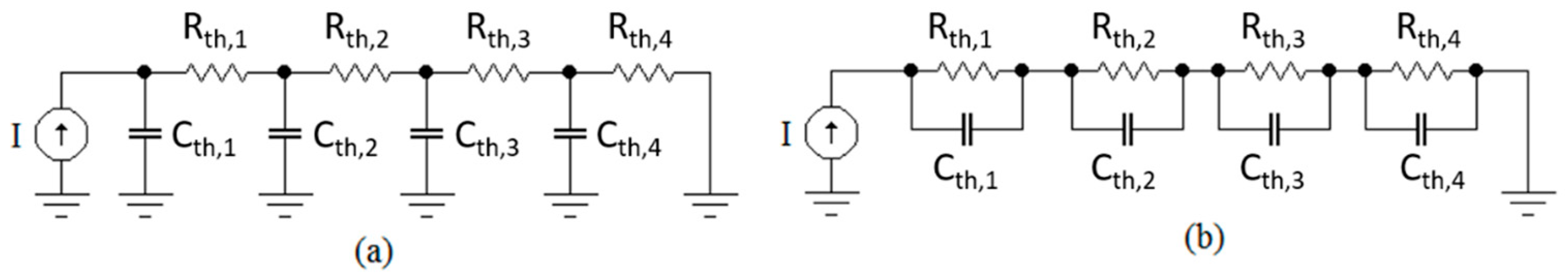
2.2. Thermal Model Concept

As discussed in [10,16,17,18], it is possible to develop thermal models by exploiting the analogies between thermal and electrical models. In such models, the electrical quantities of voltages and currents assume different physical meanings. In particular, in thermal networks, the voltage represents the temperature, while the current has the meaning of heat flow. A thermal resistance identifies an obstacle to the propagation of heat in a material, while a thermal capacitance identifies the amount of heat stored by a physical object. Therefore, it is possible to develop thermal circuit models using the Cauer or Foster networks, as discussed in [4,10,19]. Figure 2 shows the two possible network topologies. Cauer’s network is usually derived from the physical analysis of the system, while the Foster network is obtained experimentally. With both approaches, some R-C cells are used to model the thermal behavior of the different materials that constitute the physical system modelled.

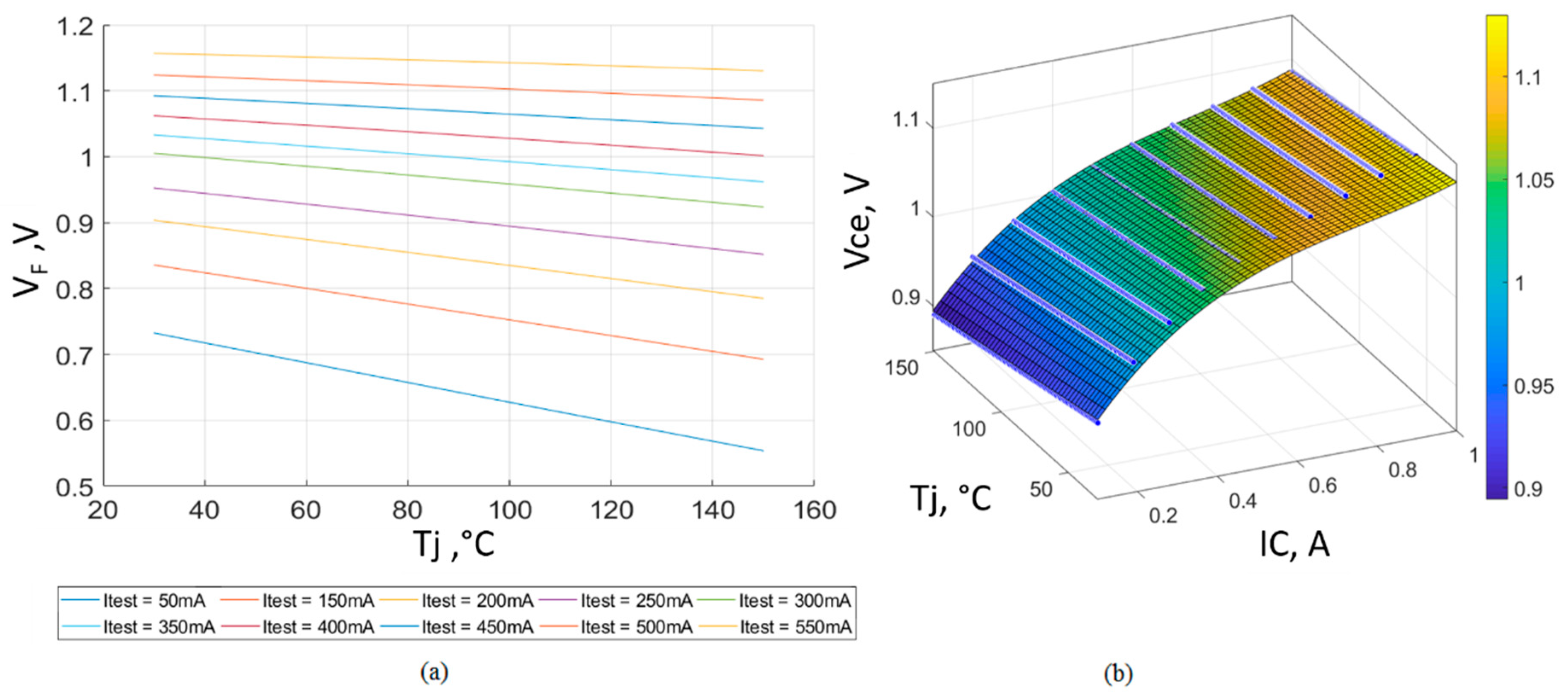
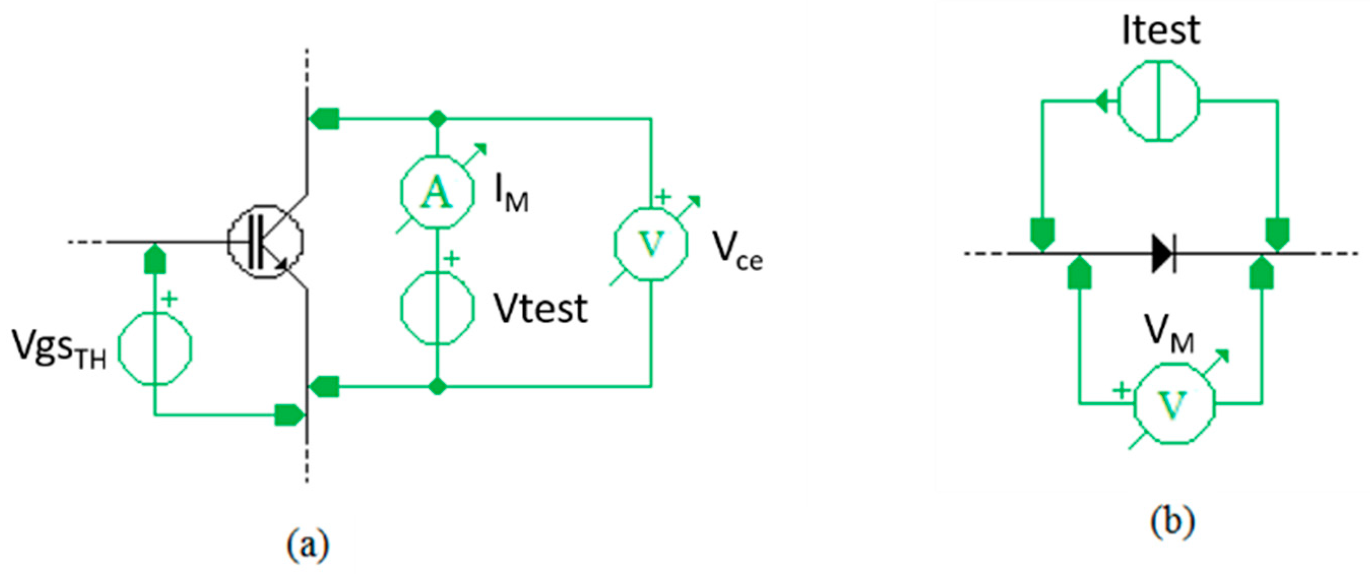
2.3. Temperature-Sensitive Electrical Parameters (TSEPs)

The measurement of the junction temperature in a semiconductor device is possible resorting to the device electrical parameters sensitive of the junction temperature. These parameters are called Temperature-Sensitive Electrical Parameters (TSEPs) [20]. In Reference [8,9], the most frequently used TSEP for measuring the Tj in the MOSFET device is considered, i.e., the relationship between the Ron of the IGBT and the Tj is discussed. In this paper, a diode and an IGBT device are considered. Among the possible TSEPs for these devices, the forward voltage (VF) of the diode and the dependence on the Vce and Ic of the IGBT are considered.
For the diode device, the relationship between VF and Tj is typically used, as discussed in [19]. In particular, there is a threshold voltage decrease as a consequence of the junction temperature increases in the diode device. Typically, the relationship VF (Tj) is provided by the diode manufacturer, or it can be obtained experimentally, as discussed in [21].
On the other side, for the IGBT device, there is a relationship that involves multiple TSEPs, as discussed in [20,22]. In particular, it is possible to estimate Tj by resorting to a relationship involving the collector–emitter voltage drop (Vce) and the Ic current that flows in the IGBT device. The relationship Vce (Ic, Tj) can be estimated with the procedure described in [22] by means of numerous electrical measurements at different Ic and Vce.

3. Proposed Approach

This section defines first the concept of thermal faults proposed by us and discusses the in-circuit test and functional test strategies considered. It then outlines the proposed approach to assess the quality of a test solution for the heatsink assembly test.

3.1. Thermal Faults

In accordance with the definition of thermal resistance provided in Section 2.2, we define the concept of thermal fault as an increase in the thermal resistance value in the thermal model of the cooling system. In the thermal model of the dissipation system, some additional thermal resistances are added in series with the thermal resistance of the model.
In this paper, we consider the thermal faults associated with the heatsink assembling; in other words, further thermal fault resistances are added in the thermal model between the portion of the model which describes the internal physical structure of the power device and the portion of the model that identifies the heatsink. Usually, as described in [23], there is a thermal contact resistance that models the difficulty that the heat encounters for propagating from the power device to the heatsink. The thermal fault resistance considered is added in series with this thermal contact resistance. From a physical perspective, the added thermal fault resistance represents a further obstacle to the propagation of the heat generated by the power device.

3.2. Thermal Faults Simulation

The effectiveness of the considered test procedures can now be assessed by means of electro-thermal simulations using a thermal model of the cooling system. The thermal model of the devices and the thermal model of the overall dissipation system can be obtained as described in [18,24,25]. The considered test methods perform voltage or current measurements on power devices; these measurements can be performed by ATE. Different thermal faults simulations are performed in a fault-free scenario and with a single thermal fault injected in the cooling system thermal model. The value of the thermal fault resistances injected is calculated as discussed in [10], i.e., the value of the thermal resistance of the fault is chosen in order to maximize the junction temperature of the power device to bring it to the maximum junction temperature supported (Tj = Tj,MAX). The value of the maximum junction temperature supported is usually provided by the power device manufacturer. As discussed in [10], a thermal resistance value equal to or greater than the thermal fault resistance brings the junction temperature of the device out of the device operating parameters defined by the device manufacturer. Values of thermal resistance lower than the thermal fault resistance cause an increase in Tj; however, the Tj remains within the thermal limits defined by the manufacturer.

3.3. TSEP Test Characterization

The evaluation of the junction temperature in the diode and IGBT devices requires an initial characterization procedure. The aim of the characterization procedure is to obtain the relationship between Tj and the electrical parameters sensitive to the Tj for the diode and the IGBT devices, as discussed in Section 2.3. Figure 3 shows the calibration circuits used for the diode and the IGBT. For the diode device, the characterization procedure was performed in two phases, a heating phase and a cooling one. In the heating phase, the switch (SW) was configured in position A.
A high current flowed through the diode in order to dissipate a high power and increase the Tj. The junction temperature reached was about the maximum junction temperature supported by the device. However, in the cooling phase, the switch was commutated in position B; a low test current was forced in the diode. During the cooling phase, the VF and Tj were continuously measured; Tj was measured on the cathode of the device, e.g., by means of a thermocouple as discussed in [26]. The power dissipated by the diode during the cooling phase was negligible; therefore, the temperature measured on the cathode was about Tj, as discussed in [26]. Figure 4a shows the trend of VF as a function of Tj for different test currents. These curves are useful for estimating the Tj during the test of the device assembled on the PCB.
Moreover, the characterization procedure for the IGBT device was performed with the circuit shown in Figure 3. The characterization procedure was similar to the diode one. However, a drive voltage higher than Vth and a voltage Val able to maintain the IGBT in conduction were imposed. In the heating phase, a high current flowed in the IGBT, while in the cooling phase, a low current was forced. Moreover, the Vce and Tj were continuously monitored in the IGBT cooling phase. The Tj was measured on the IGBT collector pin as previously discussed for the diode. Figure 4b shows the different measurements performed at different test currents during the cooling phase. The TSEP characteristic of the IGBT can be obtained by interpolating the different curves measured.

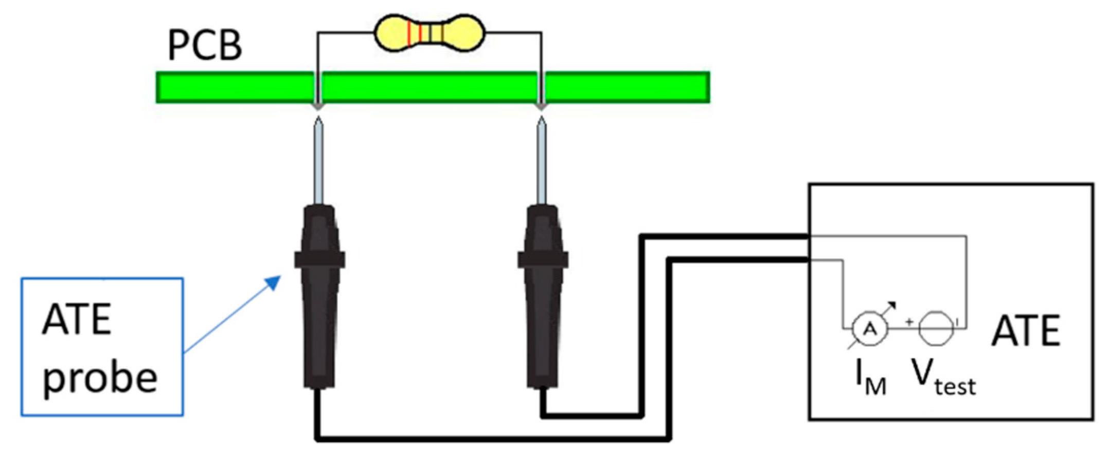
3.4. In-Circuit Thermal Test

Two different in-circuit tests procedures were considered. In this paper, we extended the methodology discussed in [9,10] to the IGBT device, while in [27], a test strategy for the diodes is shown. Both strategies consist of contacting the pins of a single power device to perform the test. Figure 5 shows the considered test procedure for a power IGBT and a diode. The circuit implemented by the ATE is indicated in green. During the in-circuit test, the PCB was not powered, and there were no further electrical stimuli applied to the PCB except those forced by the ATE. Moreover, the input and output ports of the PCB were disconnected.
For the IGBT device, two voltages were applied to turn on the device. At the same time, the ATE measured the current (IM) that flowed through the device and the voltage (Vce) between the collector and the emitter terminals. The test voltage imposed on the device was chosen considering the device specifications using Equation (1). The test voltage (Vtest) was chosen in a conservative manner in order not to damage the power device, i.e., considering 50% of the maximum power (Pmax) managed by the device. The Itest current was chosen considering the maximum current that can be delivered by the ATE during the test.
Vtest   = Pmax 2   ·   1 Itest ;   with   Itest     Imax ATE 2
With the IM and Vce values measured by the ATE, it is possible to estimate the Tj using the TSEP characterization test discussed in Section 3.3. In the presence of a thermal fault on the heatsink assembly, the Tj of the device was higher than expected; therefore, the measured IM was different from the expected one, as discussed in Section 2.3.
On the other side, for the power diode, a test current (Itest) was forced in the diode by the ATE. At the same time, the voltage drop across the diode was measured (VM). The Itest current imposed by the ATE was chosen in a conservative manner considering the device specifications. The Itest current value was chosen with Equation (2).
Itest   = Pmax 2   ·   1 V F n o m i n a l
With the VM value measured by the ATE, it is possible to estimate the Tj by means of the TSEP characterization test of the diode performed in Section 3.3. As discussed in Section 2.3 and in [27], the increase of the junction temperature in the diode device caused a decrease in the forward voltage (VF). Therefore, in the presence of a thermal fault, the voltage drop measured on the diode was lower than the expected one.

3.5. Functional Thermal Test

The functional test was performed by applying different electrical stimuli on the input ports of the power converter and observing the trend of the voltages or currents at the output ports. The proposed approach is based on the observability enhanced functional test in which the voltage drop on the power device is also measured. All measured electrical quantities must comply with the PCB specifications and must be equal (except for a defined tolerance) to the expected ones. The voltage drop on the power device is measured because it depends on the junction temperature (Tj) of the device, as discussed in Section 2.3. An excessive variation of the electrical quantities measured during the functional test indicates the presence of a thermal fault in the heatsink.

4. Case Study

In this section, the case study and the thermal model of the cooling system used are presented. In particular, a Power Supply Unit (PSU) for industrial applications was considered. The heat produced by the PSU power devices is dissipated resorting to a passive heatsink assembled on the power devices. The PCB considered was developed by the Politecnico di Torino as part of an industrial project performed by the Power Electronic Innovation Center (PEIC). The PSU considered is used to power household appliances or industrial compressors.

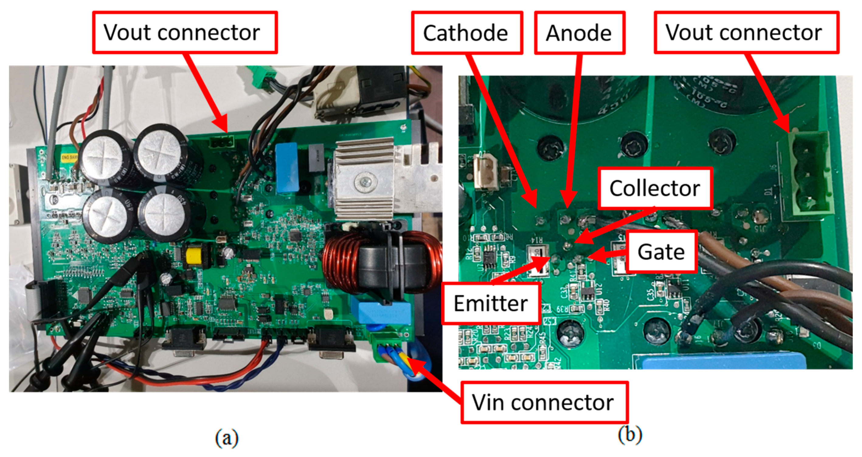
4.1. The Power Supply Unit

The PSU we considered consists of three boost cells; each cell is composed of an inductor, a diode (STTH12S06), and an IGBT (STGF19NC60), as shown in Figure 6. Figure 6 also shows the FAN9673 analog controller [28], which drives the three IGBTs of the PSU. The FAN9673 measures the currents in the three boost cells, the PSU output voltage, and the PSU input voltage in order to supply a continuous stabilized voltage in output. The currents are measured by means of appropriate sense resistances (Rs1, Rs2, Rs3). The PSU provides a DC output voltage of 400 V with a 12 A of maximum current delivered to the electrical load. The PSU works with AC sinusoidal input voltages between 110 V RMS and 220 V RMS at 50 Hz or 60 Hz. The PSU is used to power a three-phase inverter for electric motors.
The STTH12S06 diode [29] is a power device assembled in a TO-220FPAC package. It has a forward voltage (VF) of 1.5 V, and it can manage a current up to 12 A. The maximum junction temperature (TjMAX) supported is 175 °C, and it has a case junction thermal resistance (Rth,JC) of 4.6 °C/W. The IGBT STGF19NC60 [30] is a power device assembled in a TO-220FP package. The device manages voltages up to 600 V and currents up to 19 A. The maximum managed junction temperature is 150 °C with a junction-case thermal resistance (Rth,JC) of 3.9 °C/W. The STTH12S06 diode and the STGF19NC60 IGBT are produced by STMicroelectronics, while the FAN9673 analog controller is produced by ON Semiconductor.
The PSU cooling system is built using the passive SK56 heatsink produced by Fischer Elektronik [31]. The heatsink is composed of aluminum, it is equipped with numerous cooling fins able to disperse the heat. The thermal resistance of the heatsink (Rth,H_A) is 0.35 K/W. From Figure 7, it is possible to see that the heatsink completely covers the PCB of the PSU (L × W × H: 150 mm × 300 mm × 40 mm). The heatsink is connected to the three power diodes (D1, D2, D3) and to the three IGBTs (T1, T2, T3) by means of through screws. As shown in Figure 7, the PSU power diodes and IGBTs are assembled on the back side of the PCB. This configuration allows a better physical contact between the power devices and the heatsink.

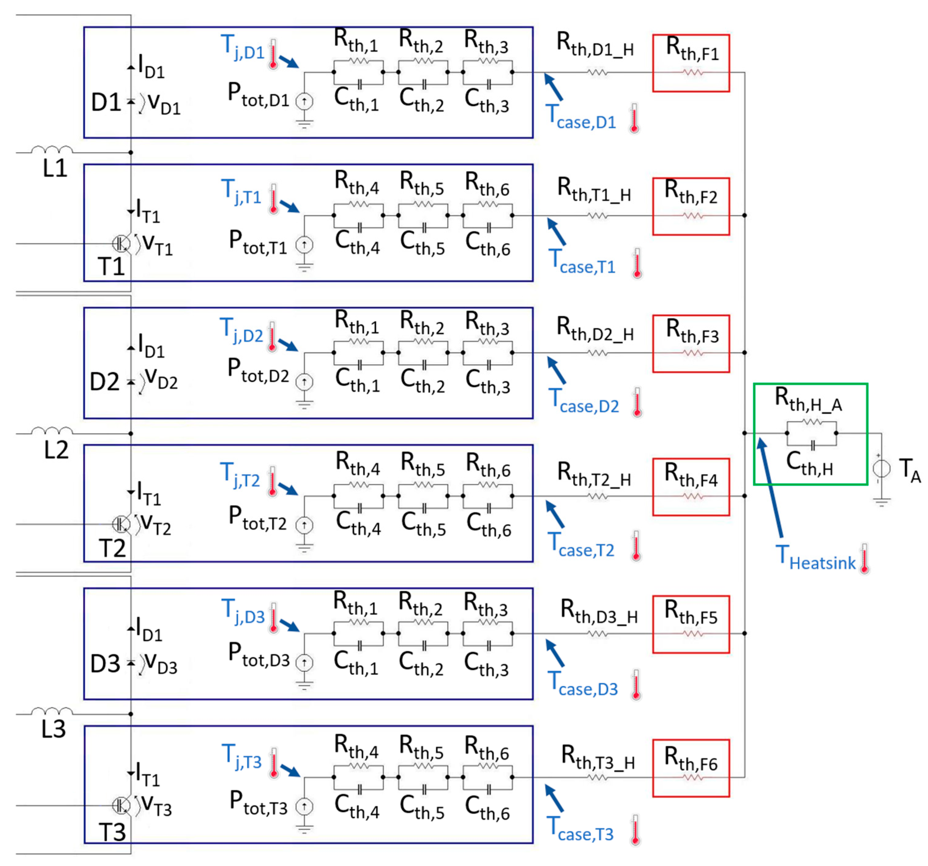
4.2. Thermal Model of the PSU Cooling System

In this sub-section, the electro-thermal models of the power devices and the cooling system of the PSU are discussed. The whole thermal model is shown in Figure 8 [18,24,25]; the three diodes and the three IGBTs that constitute the three boost cells of the PSU that share the same passive heatsink are considered, as shown in Figure 6 and Figure 7. As discussed in Reference [25], the thermal model of each device can be combined with the thermal model of the heatsink. In Figure 8, the thermal models of the power devices are shown in blue, while the thermal model of the heatsink is shown in green. Moreover, the thermal resistances (Rth,D1_H; Rth,T1_H; Rth,D2_H; Rth,T2_H; Rth,D3_H; Rth,T3_H) model the assembly of the power devices on the heatsink.
For each power device, there is a current source, called Ptot, that models the total power dissipated by the device. The power dissipated by each device is given by Equation (3) for the diode device and Equation (4) for the IGBT device, as discussed in [18]. The Ptot current generator models the heat flow produced by the power device. The thermal models of the IGBT and the diode are completed by three R-C Foster cells that model the different layers of silicon, metal, and plastic of which each device is composed. The thermal model of the single power device can be provided by the device manufacturer (an example in [17]) or obtained as proposed in [32]. An additional thermal contact resistance (Rth,D1_H; Rth,T1_H; Rth,D2_H; Rth,T2_H; Rth,D3_H; Rth,T3_H) was added between the heatsink and the case of each power device, as discussed in Section 3.1. The heatsink was modelled by an additional R-C cell (Rth,H_A; Cth,H,). Figure 8 also shows the points where the different temperatures were observed during thermal simulations; for example, the junction temperature was measured on the Ptot generator in each device. The TA voltage source was used for modelling the ambient temperature, as discussed in [17]. The six thermal fault resistances discussed in Section 3.1 are indicated in red in the thermal model (Rth,F1; Rth,F2; Rth,F3; Rth,F4; Rth,F5; Rth,F6). Each thermal fault resistance is associated with the heatsink assembled on each power device concerned. The value of the thermal fault resistances is calculated as discussed in Section 3.2.
P tot =   V D ·   I D
P tot   =   V T ·   I T

5. Results Analysis

This section shows the results obtained by means of simulations. The effectiveness of the in-circuit thermal test and functional thermal test strategies outlined in Section 3 were assessed. The test strategies were evaluated on the case study discussed in Section 4, focusing on their ability to detect possible defects affecting the heatsink assembly. In particular, the diodes and IGBTs that share the same heatsink of the PSU were considered. The last section draws some conclusions about the obtained results.

5.1. In-Circuit Thermal Test

The in-circuit thermal test was applied to the IGBTs (T1, T2, T3) and to the diodes (D1, D2, D3) of the PSU, with reference to Figure 6. The in-circuit thermal test was performed with the converter off and with the load disconnected. For the IGBT devices, the test was performed by imposing a Vtest = 1.5 V and a Vgs = 4 V on the IGBT; at the same time, the current IM that flows through the device was measured, as discussed in Section 3.3. During the test, the thermal faults (Rth,F2; Rth,F4; Rth,F6) relating to the assembling of the heatsink on the IGBTs were injected; a single fault was considered in each simulation. Table 1 shows the results obtained for the IGBT T1. Similar results were obtained on the other two IGBTs. The measurements were performed with the circuit in the steady state, i.e., when the IM current reached a stable steady-state value. An ambient temperature of 25 °C was considered during the simulation (TA = 25 V).
The considered in-circuit thermal test was able to detect the thermal fault of the heatsink assembled on the IGBT observing the IM current; in the presence of the thermal fault, the IM was larger by about 0.23 A with respect to the IM in the fault-free scenario. The value of the thermal fault resistance was chosen as discussed in Section 3.1; the value that brings the Tj,T1 of the IGBT device to the maximum junction temperature supported by the device was chosen. In this case, a thermal resistance of 10.3 °C/W was enough to bring the Tj,T1 to 150 °C.
Table 1 shows also the temperature present on the TAB transistor package (TCASE,T1) and the heatsink temperature (THEATSINK). Note that the thermal fault can also be observed resorting to the TCASE,T1 temperature of the IGBT; the TCASE,T1 temperature cannot be directly measured due to the presence of the heatsink above the power device. There is no particular variation of the heatsink temperature in presence of a fault.
Figure 9 shows the in-circuit thermal test related to the power diode D1. Similar results were obtained for the other diodes. In Figure 9, the circuit created by the ATE is shown in green. In this case, a test current of Itest = 0.5 A was forced. Table 2 shows the results obtained with the in-circuit thermal test on the diode. In presence of the fault, there was no significant VM variation from the fault-free scenario. In the case study, the in-circuit thermal test on the diodes was ineffective. It was impossible to test each diode separately due to the connection of the diodes in this circuit. The test current forced on one of the diodes by the ATE flowed on the other diodes as well. A portion of the test current forced flows through the inductances (L1, L2, L3); then the voltage drop across the three inductors was zero. Therefore, the three diodes (D1, D2, D3) were parallel; hence, they have the same voltage drop. In the presence of a thermal fault on a diode, the diode voltage drop is similar to the diode voltage drop in the fault-free scenario. The effect of the thermal fault on a diode is masked by the other diodes placed in parallel. The in-circuit thermal test is ineffective in this specific circuit due to the D1, D2, and D3 diodes placed in parallel.

5.2. Functional Thermal Test

The functional thermal test was performed by applying an AC sinusoidal voltage of 220 V RMS at 50 Hz to the input port of the power converter. A resistor was connected to the output port as an electrical load. The test was performed using the observability enhanced functional test strategy discussed in Section 3.4; therefore, during the test, it was possible to measure other electrical quantities by placing additional probes on the PCB. Typically, voltage measurements are performed on the PCB. During the test, different electrical quantities were measured, such as the IL current that flows through the RL load, the current IA absorbed by the PSU, the output voltage Vout of the PSU, the IGBT voltage Vce when the IGBT was saturated, and VF on the diode when the diode was directly polarized. Table 3 shows the measured values in the fault-free scenario and in presence of the heatsink thermal fault for the IGBT device, while Table 4 shows the measured values for the diode device. The electrical quantities IL, IA, Vout, Vce, and Vak were measurable by ATE during the test, while the other measurements were obtained only in simulation. Furthermore, Table 3 and Table 4 show the junction temperature reached in the power device, the device case temperature, and the heatsink temperature. The values shown in Table 3 and Table 4 refer to the IGBT T1 and the diode D1, while similar values were also measured for the other devices.
The base functional test approach was performed observing only the signals at the PCB input/output ports; in the case study, the IL current on the electrical load, the IA current absorbed by the PSU from the electrical grid, and the Vout voltage provided by the PSU were considered. With the base functional test approach, no thermal faults were detected, as shown in Table 3 and Table 4. With the observability enhanced functional test approach, it was possible to observe the effect of the thermal fault on the heatsink assembly, as shown in Table 3 and Table 4. In particular, it was possible to detect the faults by measuring the voltage drop (Vce,T1; VF,D1) present on the power devices.

5.3. Tests Results

This last section summarizes the main results obtained with the in-circuit thermal test and with the functional thermal test. Table 5 shows, for each test strategy, which thermal faults were detected (DT) or not detected (NDT).
The in-circuit thermal test is potentially able to detect the thermal faults associated with the heatsink assembly on the power devices, provided that the PCB circuit allows the test, in other words, if the stimuli applied by the ATE on the power device are not influenced by other devices present in the circuit, e.g., the D1, D2, and D3 diodes in the case study. In addition, to perform the in-circuit thermal test, the ATE probes must be able to physically reach each device. The physical access to the power device can be inhibited by the power heatsink itself that covers the power device. During the development of the PCB, it was possible to introduce some test points that were used by ATE to contact the power devices of interest, as discussed in Section 2.1. This location is specifically designed to be accessible by ATE also in the presence of a heatsink.
The base functional test was not sufficient to observe the thermal faults considered. The electrical quantities observed during the base functional test were controlled by the FAN9673 controller. The analog controller of the PSU aims to stabilize the PSU output voltage and to maintain a constant absorption from the electrical network. Therefore, the base functional test approach may not be sufficient in closed-loop electric systems. The Observability enhanced functional test was able to detect the thermal faults considered, but it had the same problem of physical accessibility to the device already discussed for the in-circuit thermal test. Figure 10 shows the pins of the power devices accessible by ATE for the PCB case study.
The simulations were performed using the PLECS circuit simulator [33]. PLECS is a behavioral simulator specifically designed for simulating power circuits. Each simulation required about 20 min of CPU time on a PC equipped with an 8-core AMD FX-8370 processor operating at 4 GHz and 32 GB of 1333 RAM memory.

6. Conclusions

The growing use of power electronics in safety-critical applications requires accurate test strategies even for those aspects usually not considered, such as the heatsinks assembled on the power devices. The junction temperature increase is the main cause of ageing, mechanical stress, and breakage of the power devices. This paper highlights the importance of testing some aspects normally not considered, such as heatsinks. An incorrect assembly of the heatsink causes an increase of the temperature inside of the power devices. This paper reiterates the concept of thermal fault associated with the heatsink assembly. Some thermal fault resistances were considered in the thermal model of the cooling system. The values of the thermal fault resistances were calculated so as to bring the junction temperature of the power device to the maximum temperature supported, i.e., outside the operating parameters defined by the device manufacturer.
The paper proposes a methodology to assess the effectiveness of different test strategies using a thermal model of the cooling system. Some thermal faults associated with the heatsink assembly were considered in the cooling system thermal model. The results obtained with the different test strategies can be compared for identifying the best test strategy among those considered.
In this paper, we consider three different test strategies to detect the presence of thermal faults associated with the heatsink’s assembly. The considered tests strategies are based on the in-circuit test and the functional test. The tests considered can be easily performed by ATE on the final PCB. The advantages and disadvantages of the three test strategies were evaluated in an industrial case study. In particular, the in-circuit test strategy can be used when the circuit allows it, i.e., when the test is not inhibited by any other devices present on the PCB. The base functional test approach is not able to detect thermal faults; it is necessary to use an improved version of the basic functional test approach as the observability enhanced functional test. The observability enhanced functional test strategy allows for the identification of the thermal faults when it is possible to perform further measurements on the PCB during the functional test. Moreover, it is possible to introduce additional test points on the PCB during the PCB design phase. These test points allow the ATE to perform measurements in points normally inaccessible on the PCB. It should be remembered that the addition of test points increases the PCB complexity because it introduces additional traces on the PCB. As a case study, a PSU composed of different power devices was considered.

Author Contributions

Methodology, D.P. and M.V.Q.; investigation, D.P. and M.V.Q.; resources, S.B. and E.G.A.; writing, D.P., S.B., M.V.Q., M.S.R., E.G.A. and F.F.; supervision, F.F., M.S.R. and E.G.A.; All authors have read and agreed to the published version of the manuscript.

Funding

This research received no external funding.

Acknowledgments

The research activity was supported by the Power Electronics Innovation Center (PEIC) of the Politecnico di Torino.

Conflicts of Interest

The authors declare no conflict of interest.

References

  1. Jose, J.; Ravindran, A.; Nair, K.K. Study of temperature dependency on MOSFET parameter using MATLAB. Res. J. Eng. Technol. 2016, 3, 1530–1533. [Google Scholar]
  2. Baodong, B.; Dezhi, C. Inverter IGBT loss analysis and calculation. In Proceedings of the 2013 IEEE International Conference on Industrial Technology (ICIT), Cape Town, South Africa, 25–28 April 2013; pp. 563–569. [Google Scholar]
  3. Vassighi, A.; Sachdev, M. Thermal and Power Management of Integrated Circuits; Springer: Berlin/Heidelberg, Germany, 2006; ISBN 978-1-4419-3832-9. [Google Scholar]
  4. Chen, H.; Ji, B.; Pickert, V.; Cao, W. Real-time temperature estimation for power MOSFETs considering thermal aging effects. IEEE Trans. Device Mater. Reliab. 2014, 14, 220–228. [Google Scholar] [CrossRef]
  5. Dusmez, S.; Duran, H.; Akin, B. Remaining useful lifetime estimation for thermally stressed power mosfets based on on-state resistance variation. IEEE Trans. Ind. Appl. 2016, 52, 2554–2563. [Google Scholar] [CrossRef]
  6. Russo, S.; Bazzano, G.; Cavallaro, D.; Sitta, A.; Calabretta, M. Thermal analysis approach for predicting power device lifetime. IEEE Trans. Device Mater. Reliab. 2019, 19, 159–163. [Google Scholar] [CrossRef]
  7. High-Power Device. Toshiba Application Note 2016-12-05. Available online: https://www.google.com/url?sa=t&rct=j&q=&esrc=s&source=web&cd=1&ved=2ahUKEwithNvTq_7nAhWQCOwKHQ77CVQQFjAAegQIBBAB&url=https%3A%2F%2Ftoshiba.semicon-storage.com%2Finfo%2Fdocget.jsp%3Fdid%3D60472&usg=AOvVaw2GiUlKBN7lxE7civ593myo (accessed on 12 May 2016).
  8. Mersen, Cooling of Power Electronics—Solutions for Power Management. Available online: https://www.mersen.com/sites/default/files/publications-media/4-spm-cooling-of-power-electronics-mersen.pdf (accessed on 1 January 2017).
  9. Quitadamo, M.V.; Piumatti, D.; Sonza Reorda, M.; Fiori, F. Faults detection in the heatsinks mounted on power electronic transistors. Inter. J. Electr. Electron. Eng. Telecommun. 2020, 9, 206–212. [Google Scholar] [CrossRef]
  10. Piumatti, D.; Quitadamo, M.V.; Sonza Reorda, M.; Fiori, F. testing heatsink faults in power transistors by means of thermal model. In Proceedings of the 2020 IEEE Latin-American Test Symposium (LATS), Maceio, Brazil, 30 March–2 April 2020; pp. 1–6. [Google Scholar]
  11. Khandpur, R.S. Printed Circuit Boards Design, Fabrication, and Assembly; McGraw-Hill Education Book: New York, NY, USA, 2005; ISBN 0071331476. [Google Scholar]
  12. Coombs, C.; Holden, H. Printed Circuits Handbook, 7th ed.; McGraw-Hill Education Book: New York, NY, USA, 2016; ISBN 9780071833950. [Google Scholar]
  13. Introduction to the In-Circuit Testing. GenRad. 1984. Available online: https://www.ietlabs.com/pdf/Handbooks/Introduction%20to%20In-Circuit%20Testing.pdf (accessed on 1 January 1984).
  14. Crandall, E. Power Supply Testing Handbook: Strategic Approaches in Test Cost Reduction; Springer: Berlin/Heidelberg, Germany, 1997; ISBN 978-1-4615-6055-5. [Google Scholar]
  15. Piumatti, D.; Borlo, S.; Mandrile, F.; Reorda, M.S.; Bojoi, R. Assessing the effectiveness of the test of power devices at the board level. In Proceedings of the 2019 XXXIV Conference on Design of Circuits and Integrated Systems (DCIS), Bilbao, Spain, 20–22 November 2019; pp. 1–6. [Google Scholar]
  16. Thermal Modeling of Power-electronic Systems. Dr. Martin März, Fraunhofer Institute for Integrated Circuits IIS-B, Erlangen Paul Nance, Infineon Technologies AG, Munich, Document. Available online: https://www.iisb.fraunhofer.de (accessed on 1 February 2000).
  17. Thermal System Modeling. Dr. Martin März, Paul Nance, Infineon Technologies AG, Munich, Document. Available online: https://www.infineon.com (accessed on 1 February 2000).
  18. Shahjalal, M. Electric-thermal Modelling of Power Electronics Components. Ph.D. Thesis, University of Greenwich, London, UK, 2018. Available online: https://gala.gre.ac.uk/id/eprint/23658/1/Mohammad%20Shahjalal%202018%20-%20secured.pdf (accessed on 1 April 2018).
  19. Altet, J.; Rubio, A. Thermal Testing of Integrated Circuits; Springer Book: Berlin/Heidelberg, Germany, 2002; ISBN 978-1-4419-5287-5. [Google Scholar]
  20. Sathik, M.H.M.; Pou, J.; Prasanth, S.; Muthu, V.; Simanjorang, R.; Gupta, A.K. Comparison of IGBT junction temperature measurement and estimation methods-a review. In Proceedings of the 2017 Asian Conference on Energy, Power and Transportation Electrification (ACEPT), Singapore, 24–26 October 2017; pp. 1–8. [Google Scholar]
  21. Kadir, E.; Songül, D.; Nuhoglu, C.; Urhan, F.; Turut, A. Effect of temperature on the current (capacitance and conductance)–voltage characteristics of Ti/n-GaAs diode. J. Appl. Phys. 2014, 116, 234503. [Google Scholar]
  22. Cao, H.; Ning, P.; Yuan, T.; Wen, X. Online monitoring of IGBT junction temperature based on vce measuremnt. In Proceedings of the 2019 22nd International Conference on Electrical Machines and Systems (ICEMS), Harbin, China, 11–14 August 2019; pp. 1–5. [Google Scholar]
  23. Andrew Sawle and Arthur Woodworth Mounting Guidelines for the Super-247, International Rectifier, Application Note AN-997. Available online: https://www.fer.unizg.hr/_download/repository/ineu_sasa/06_Hladnjaci/Predavanje-Spoj_tr_na_hladnjak.pdf (accessed on 22 May 2020).
  24. Künzi, R. Thermal Design of Power Electronic Circuits. In Proceedings of the CAS-CERN Accelerator School: Power Converters, Baden, Switzerland, 7–14 May 2014. [Google Scholar]
  25. Zhou, Z.; Holland, P.M.; Igic, P. Compact thermal model of a three-phase IGBT inverter power module. In Proceedings of the 2008 26th International Conference on Microelectronics, Nis, Serbia & Montenegro, 11–14 May 2008; pp. 167–170. [Google Scholar]
  26. Thermal Design of Light Emitting Diode” NICHIA, Application Note, SE-AP00002. 15 June 2011. Available online: https://www.nichia.co.jp/specification/products/led/ApplicationNote_SE-AP00002-E.pdf (accessed on 22 May 2020).
  27. Ocaya, R. An experiment to profile the voltage, current and temperature behaviour of a P–N diode. Eur. J. Phys. 2006, 27, 625. [Google Scholar] [CrossRef]
  28. FAN9673 Three-Channel Interleaved CCM PFC Controller, Datasheet. Available online: https://www.onsemi.com/pub/Collateral/FAN9673-D.PDF (accessed on 1 June 2019).
  29. STTH12S06 STMicroelectronics Datasheet. Available online: https://www.st.com/resource/en/datasheet/stth12s06.pdf (accessed on 1 October 2007).
  30. STDGB19NC60HDT4 Power IGBT developed by STMicroelectronics, Datasheet. Available online: https://www.st.com/resource/en/datasheet/stgb19nc60hdt4.pdf (accessed on 1 September 2016).
  31. SK 56 Heatsink Datasheet Produced by Fischer Elektronik, Datasheet. Available online: https://www.fischerelektronik.de/web_fischer/en_GB/heatsinks/A01/Standard%20extruded%20heatsinks/PR/SK56_/$productCard/parameters/index.xhtml (accessed on 13 October 2006).
  32. Merrikh, A.; McNamara, A.J. Parametric evaluation of foster RC-network for predicting transient evolution of natural convection and radiation around a flat plate. In Proceedings of the Fourteenth Intersociety Conference on Thermal and Thermomechanical Phenomena in Electronic Systems (ITherm), Orlando, FL, USA, 27–30 May 2014. [Google Scholar]
  33. PLECS Tool Reference. Available online: https://www.plexim.com/home (accessed on 5 January 2020).
Figure 1. In-circuit test approach.
Electronics 09 01020 g001
Figure 2. (a) Cauer thermal network; (b) Foster thermal network.
Electronics 09 01020 g002
Figure 3. Diode (a) and Insulated Gate Bipolar Transistor (IGBT) (b) characterization circuits.
Electronics 09 01020 g003
Figure 4. (a) Diode Temperature-Sensitive Electrical Parameters (TSEP), (b) IGBT TSEP.
Electronics 09 01020 g004
Figure 5. (a) In-circuit thermal test for IGBT device; (b) in-circuit thermal test for diode device.
Electronics 09 01020 g005
Figure 6. The Power Supply Unit (PSU).
Electronics 09 01020 g006
Figure 7. (a) Printed Circuit Board (PCB) overview; (b) power devices assembled between the PCB and the heatsink.
Electronics 09 01020 g007
Figure 8. Thermal model of the cooling system.
Electronics 09 01020 g008
Figure 9. In-circuit thermal test for diode device.
Electronics 09 01020 g009
Figure 10. (a) PCB surface; (b) Contact points accessible from the Automatic Test Equipment (ATE).
Electronics 09 01020 g010
Table 1. In-circuit IGBT results.
Rth,F2 (°C/W)IM (A)Vce,T1 (V)Tj,T1 (°C)TCASE,T1 (°C)THEATSINK (°C)
Fault-free01.041.41724226
With fault10.31.271.4314811725
Table 2. In-circuit diode results.
Rth,F1 (°C/W)VM (V)Tj,D (°C)TCASE,D1 (°C)THEATSINK (°C)
Fault-free01.4631.227.225.4
With fault16.71.45176.351.725.5
Table 3. Results for the functional test of the IGBT.
Rth,F2 (°C/W)IL (A)IA (A)Vout (V)Vce,T1 (V)Tj,T1 (°C)TCASE,T1 (°C)THEATSINK (°C)
Fault-free08.516.14000.7571.133.728.3
With fault10.38.516.14001.21151.286.328.5
Table 4. Results for the functional test of the diode.
Rth,F1 (°C/W)IL (A)IA (A)Vout (V)VF,D1 (V)Tj,D1 (°C)TCASE,D1 (°C)THEATSINK (°C)
Fault-free08.516.14001.382.938.428.2
With fault16.78.516.14001.1181.195.628.4
Table 5. Test approach comparisons.
Thermal FaultPower DeviceIn-CircuitBase Functional TestObservability Enhanced Functional Test
Rth,F1; Rth,F3; Rth,F5Diodes D1, D2, D3NDTNDTDT
Rth,F2; Rth,F4; Rth,F6IGBTs T1, T2, T3DTNDTDT

