Article

Open-Air Processing of Mechanically Robust Metal Halide Perovskites with Controllable Thicknesses above 10 µm

by
Kayshavi Bakshi
,
Muzhi Li
,
Muneeza Ahmad
,
Mason Mahaffey
and
Nicholas Rolston
*
Renewable Energy Materials and Devices Lab, School of Electrical, Computer and Energy Engineering (ECEE), Arizona State University, Tempe, AZ 85284, USA
*
Author to whom correspondence should be addressed.
Processes 2024, 12(9), 1901; https://doi.org/10.3390/pr12091901
Submission received: 26 July 2024 / Revised: 23 August 2024 / Accepted: 27 August 2024 / Published: 5 September 2024

Abstract

:
We report on the use of open-air blade-coating as a scalable method for producing metal halide perovskite films with >10× fracture energy for durability and mechanical stability through the addition of corn starch polymer additives. This results in a manufacturable and robust perovskite that has tunable thicknesses exceeding 10 µm, among the highest reported values for solution-processed polycrystalline films. We find that an increasing amount of starch causes more uniform carbon distribution within the perovskite thickness as quantified by cross-sectional elemental composition measurements. Further, the incorporation of starch introduces beneficial compressive film stresses. Importantly, the optoelectronic behavior is not compromised, as the photoluminescence spectrum becomes more homogenous with the addition of corn starch up to 20% by weight.

Graphical Abstract

1. Introduction

Up until recently, the mechanical properties and durability of perovskites were long disregarded. Many recent studies have focused on strain engineering perovskites to reduce internal degradation and improve optoelectronic properties. The fracture energy (Gc) is now being studied more commonly to better understand the mechanical properties of Perovskite Solar Cells (PSCs) and perovskite films [1,2,3,4,5,6,7,8,9]. The fracture energy, Gc, is the strain energy per unit area that is required to generate a crack through a material and quantifies the robustness or durability of materials. Gc is dependent on two processes: plastic deformation and atomic bond breakage. Within materials that are plastically deformable, the energy to break their atomic bonds is generally much lower than the energy needed for plastic deformation. However, due to their fragile and brittle nature, the Gc of perovskites is largely due to atomic bond breakage. In fact, perovskites have such weak ionic bonding that their Gc is often comparable to table salt. Furthermore, the thin film layers that make up PSCs—including the perovskite itself—are susceptible to high stresses and strain-induced delamination [10]. This is due to the weak, low-adhesion bonds between the layers, especially when small molecules are involved such as fullerenes. The stresses and weak bonds within the films can eventually lead to fracture and layer delamination within the material. Fracturing and delamination of PSCs can further damage the device and accelerate environmental degradation by allowing moisture and loss of the organic cations in the perovskite structure. Accelerated degradation caused by fracture and delamination can result in the loss of ohmic contact, leading to compromises in power conversion efficiency (PCE) and device failure.
PSCs have quickly developed over the last 10–15 years. They have improved from a 3.8% record PCE to >25% record PCE in just over a decade [11,12,13,14]. Yet, PSCs are currently not competitive with their silicon alternatives when it comes to their long-term operational stability. Past studies have found that the fracture energy of PSCs is consistently <1.5 J/m2, while c-Si cells are ~10–200 J/m2 [10]. The robust covalent bonds between silicon atoms enable higher toughness, leading to >25-year operational lifetimes above 80% of their initial performance [15]. Investigating the fracture energy of perovskite is, therefore, significant in increasing their operational longevity.
Along with operational longevity, scaling PSC manufacturing is another important factor for the future of these devices. Currently, different film fabrication techniques are used between lab and industry, with no dominant method emerging for long-term scaled perovskite manufacturing [16]. Spin coating is a film fabrication technique that has been widely used to create uniformly dense and stable perovskite films but is restricted to the physical substrate size [17]. Other fabrication methods, such as blade-coating and slot-die coating, are particularly promising due to their ability to be performed in the open air on flexible substrates, their affordability, and their industrial scalability [18,19]. However, this comes with the challenge of controlling film crystallization since the use of an antisolvent is challenging. Many studies have discussed solvent engineering and quenching approaches to enable PSCs with blade-coating and the similarly designed slot-die coating technique [20,21,22].
Additive engineering is a method that can be used to improve both the robustness and scalability of perovskite. The addition of starch additives to perovskite also aids in the fabrication of a film with controlled crystallization in a single antisolvent-free and quench-free step using blade-coating. The incorporation of polymer additives, such as corn starch or gellan gum, enables the tuning of various properties of perovskite and shows promising effects in reducing film degradation and aiding in stability [23]. Specifically, it has been shown that a small amount of ionic liquid additive to the perovskite precursor aided in passivating non-radiative recombination due to defects at the grain boundaries [23]. It was shown that the incorporation of starch into perovskite imparts hygroscopic abilities that protect the perovskite from moisture and the ambient environment [24,25]. Other work observed a retention of 50% of initial PCE after aging tests of spin-coated MAPI films with starch additive, credited to the protection effect from ambient contamination from the hygroscopic starch [24]. The same study found that the addition of starch enabled the formation of a high-quality film with optimized band energy alignment, resulting in a respectable PCE of 18.8%, demonstrating the ability of non-conductive additives that do not compromise device performance [24]. Regarding robustness and stability, the plasticity of corn starch improves the resistance of the perovskite to bending stresses. Previous reports suggest that corn starch aids in trapping the cation and reducing structural decomposition, resulting in a more stable film under thermal cycling and moderate humidity when compared to unmodified perovskite [24,25]. Additive engineering with starch and similar non-conducting polymers has also shown promising results in improving operational stability. One study tested gellan gum and starch additives in MAPI films in aging conditions at 85% humidity for 100 h. These samples with additives took longer to visibly degrade, displaying the improved stability both starch and gellan gum impart on MAPI films [7]. Another experiment involving the thermal cycling of MAPI with additives between −40 and 85 °C for 200 cycles supports the additives’ ability to stabilize the perovskite films due to inducing compressive intrinsic stresses within the film [7]. Compressive film stresses are one of the desirable film properties when fabricating perovskite devices as they impart self-healing properties and stability to the perovskite film. A critical aspect of film fabrication is tuning the thickness of the perovskite for optimal properties such as film morphology, power conversion efficiency, and stability. Previously, the thickness of spin-coated perovskite films was controlled by molarity and concentration adjustments of the precursors or spin speed [26,27,28]. These methods allow easy control of film thicknesses that range from a few hundred nanometers to 1 µm. The incorporation of additives to the perovskite structure offers a new avenue to engineer the viscosity of the precursor solution and fabricate thicker films (1–15 µm thick). The addition of corn starch and polymer additives to perovskite precursor results in more viscous solutions, allowing for better control over deposition and coverage using blade-coating methodology. The creation of thicker films is particularly useful for high-energy detection applications such as X-ray and alpha/beta radiation detection, as recent work has demonstrated tuning the viscosity of the ink to enable ultra-thick (~100 µm) films using CsPbBr3 [29]. This is desirable because the thicker the active layer in an X-ray detector, the higher the direct absorption of high-energy species will be [30]. Furthermore, perovskites are well-suited for higher absorption applications due to the composition of large atomic number elements such as lead [Pb] and iodine [I] [31,32]. In addition, the large radiation resistance, processing versatility, and their defect tolerant nature make perovskites a great potential candidate for high energy detection [30,31,33,34,35,36].
In this work, we study the effect of a corn starch additive on the mechanical properties, stability, and microstructure of methylammonium lead iodide, CH3NH3PbI3 (MAPI). We investigate the elemental composition and optical property changes that occur with the addition of corn starch with the use of X-ray diffraction and photoluminescence testing. The objective of this research was to improve mechanical durability and develop a scalable, open-air fabrication method of MAPI perovskite films through the incorporation of corn starch polymers. Altogether, this study utilizes processing techniques and solution–additive engineering to simultaneously improve the robustness of perovskite and ensure future scalability.

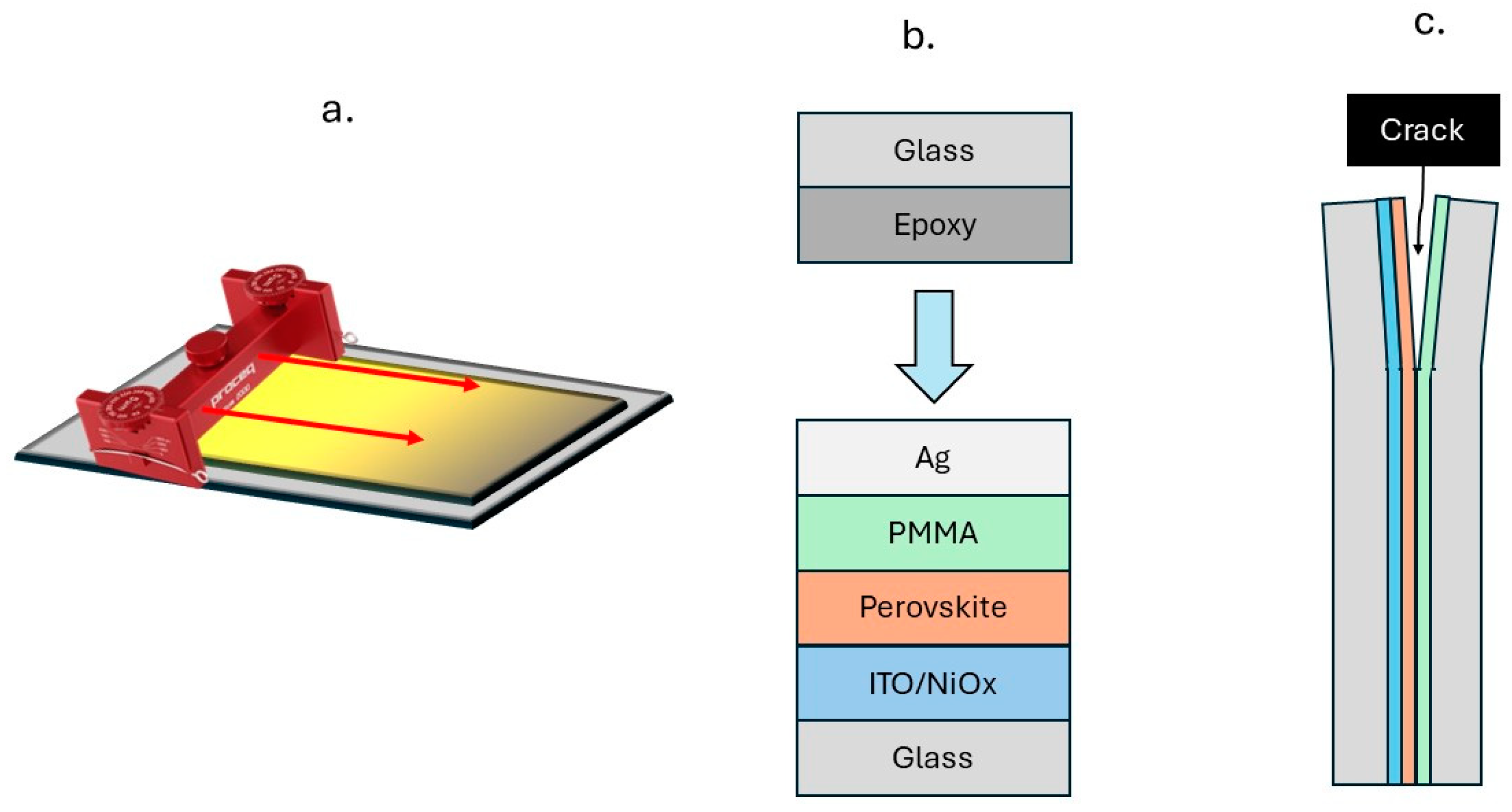
2. Materials and Methods

The MAPI ink is made by combining MAI and PbI2 in a ratio of 159 mg MAI: 461 mg PbI2 to 1 mL Dimethyl Sulfoxide (DMSO). This solution is then mixed in a FisherBrand Vortex Mixer until homogenous. Once these perovskite precursors are dissolved, they can be used to make the 5 wt%, 10 wt%, and 20 wt% starch weight concentration inks. Specifically, to make a 5% weight concentration, 31 mg of starch was added to 1 mL of 1.0 M MAPI ink. The MAI was acquired from GreatCell Solar, Queanbeyan, Australia and the PbI2 from TCI, Portland, OR, USA. The corn starch and DMSO were acquired from Sigma Aldrich Inc, St. Louis, MO, USA. After adding the starch to the inks, they are then placed on a magnetic hot plate with a stir bar to mix until the starch is integrated into the inks. To make the fracture samples, the ink is deposited (20–30 µL) through blade-coating at a speed of 4 × 25 mm/s on a preheated glass substrate (40 °C) and annealed at 100 °C for 30 min (Figure 1a). The glass substrates are at least 3 cm long to promote multiple fractures throughout testing. The glass substrate shall either have a layer of Nickel Oxide (NiO, spin-coated) or be ITO glass (Indium Tin Oxide) to create roughness. Once the perovskite ink is deposited on the glass substrate, two protective layers are then deposited. These protective layers are to prevent epoxy deformation from contributing to the perovskite fracture energy. Tested samples had layers where both layers were polymethyl methacrylate (PMMA) or with 1-layer PMMA and 1-layer of evaporated silver (Ag) (Figure 1b). The NiO and PMMA layers are spin-coated to evenly distribute the compound across the film. To finish creating a double cantilever beam (DCB) fracture testing sample, a thin layer of epoxy is layered onto an identical-sized glass substrate and bonded to the PSC film. The epoxy is then left to cure overnight at room temperature in an N2 Box. The final fracture testing sample is a sandwich-like structure where the PSC film layers are between two glass substrates.
Using double cantilever beam testing (DCB), the critical load that is necessary for fracture propagation is found alongside the Gc value. The sandwiched structure samples are tested by the DCB. A necessary part of this fracture testing is creating a pre-crack in the sample to assist crack formation at the perovskite layer. A pre-crack is made by carefully inserting the tip of a razor in between the sandwiched sample and creating a well-defined crack between the two glass substrates (Figure 1c).
Next, the sandwiched sample is loaded in the DCB system with a constant displacement rate until the load suddenly decreases. This sudden decrease represents the critical load that starts the crack propagation throughout the sample. After the sudden drop in load occurs, the sample is then unloaded briefly to obtain a linear region for calculating the crack length. Then, the sample is re-loaded until the next sudden drop in load. The process is then repeated to propagate the crack throughout the sample in cycles. In cycling the sample through loading and unloading cycles, there are additional critical loads correlating with the propagating crack. The Gc can then be calculated for each of these critical loads and averaged to maximize the data per sample using this equation:
G c = 12 P c 2 a 2 b 2 E h 3   1 + 0.64 h a 2
Pc is the critical load that deviates from the linear elastic region of the material in the load-displacement plot, a is the crack length that is calculated using the compliance method, b and h are the width and height of the sample, and E is the elastic modulus of the glass substrate. The crack length, a, can be calculated using the following equation:
a = d Δ d P B E h 3 8 1 3 0.64 h 2  
where Δ is displacement and P represents the applied load. The above equations are used to find the fracture energy as a function of the critical loads it takes to propagate a crack through a material or device stack. In simple terms, fracture energy is calculated from the energy needed from contributions of breaking bonds and deformation of material, which is, in this case, a MAPI film.
The XRD-sin2 ψ method was used to measure the residual perovskite film stress. This method conducts XRD scans of the sample at various fixed tilt angles (ψ) and emits diffraction angles (2θ) [37,38]. After calibrating the XRD tool and aligning the sample, an initial 2θ scan was taken across a wide range (5–55°). From there, a high-angle, high-intensity peak is selected to perform the psi measurements. Scans of the sample are then performed at that peak at a wide range of values of sin2ψ (sin2ψ = 0, 0.05, 0.1, 0.15, 0.2, 0.25, 0.3). For the MAPI used in these experiments, a 2θ peak at 20 was used to perform sin2ψ measurements; 2θ is then used to define dϕψ (d-spacing of the crystal lattice) that is used in a linear regression of Equation (4) to calculate stress. The relationship between 2θ and dϕψ is defined by Bragg’s law:
d ϕ ψ = λ 0 2 sin 2 θ  
where λ0 is the characteristic wavelength of the incident X-rays used in the XRD analysis. For this analysis, a λ0 of 0.154 nm was used. Once d-spacing is found with Bragg’s relationship with 2θ, the sin2ψ equation below can be used to plot linear regression of d-spacing vs. [(1 + ν) ∗ sin2ψ − 2ν]/E:
d ϕ ψ = 1 + v f E f sin 2 ψ 2 v f E f σ f d 0 + d 0  
Ef is the Young modulus of the film, νf is the Poisson ratio of the film, σf is the stress within the film, d0 is the lattice spacing at the stress-free or unstrained condition, and dϕψ is the lattice spacing of the measured plane. For MAPI, the Poisson ratio and Young’s modulus used was 0.33 and 15 GPa, respectively. Measuring the peak shifts of the perovskite at different detector tilt angles allows an understanding of how the lattice deforms with the addition of starch. From this equation, residual film stress can be calculated by dividing the slope (σf d0) by the y-intercept (d0).
The Delaminator Adhesion Test Systems (DTS, Menlo Park, CA, USA) is used in DCB configuration to conduct fracture tests. A Horiba GD-Profiler 2 Glow Discharge Optical Emission Spectrometer (Horiba, Irvine, CA, USA) was used to obtain composition profiles of the perovskite films. Using a Tencor P-16 Profilometer (KLA, Milpitas, CA, USA) and scoring our varying samples, the thickness of these blade-coated samples was found. A Rigaku Smart Lab X-ray diffractometer (Rigaku, Tokyo, Japan) was used for X-ray diffraction sin2ψ analysis. A Photon Etc. IMA Hyperspectral Imager (Photon Etc, Montreal, QC, Canada) was used to gather hyperspectral photoluminescence images.
Hyperspectral photoluminescence (PL) measurements were taken using a Photon Etc. IMA hyperspectral microscope [39]. By using a Volume–Bragg grating to select for specific wavelengths, this microscope captures calibrated PL spectra at each pixel of an imaging camera. A 660 nm laser was used to illuminate the sample under a 20× objective. The photon flux at the sample was calibrated to be approximately 1-Sun equivalent by using a Thorlabs PM100D laser power meter (along with knowledge of the illumination area and the assumption that the laser power was perfectly absorbed by the samples). Each image displays an area of approximately 385 μm × 385 μm.

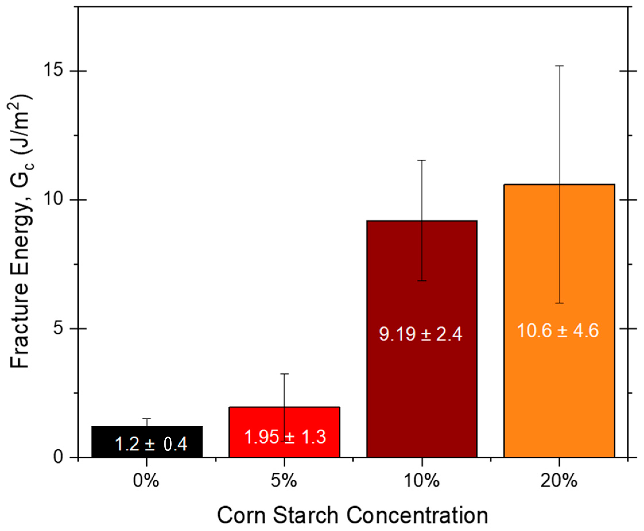
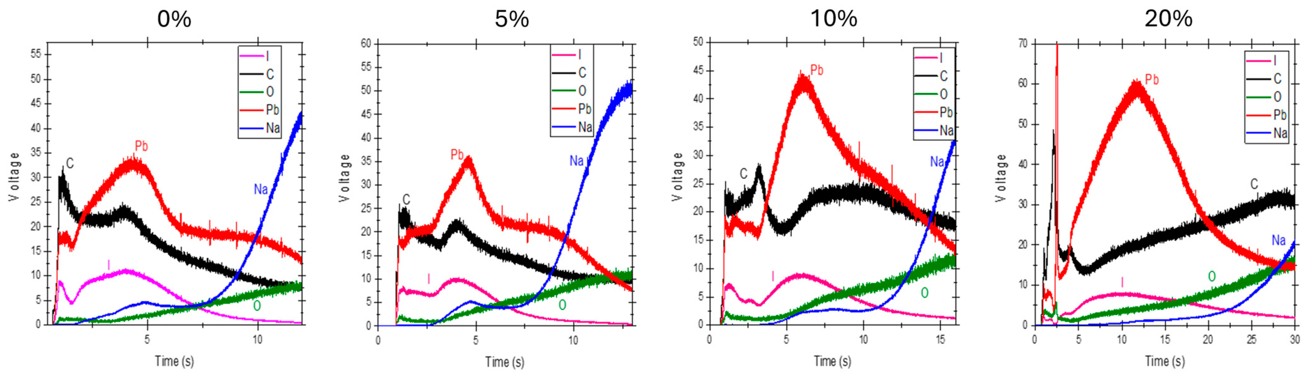
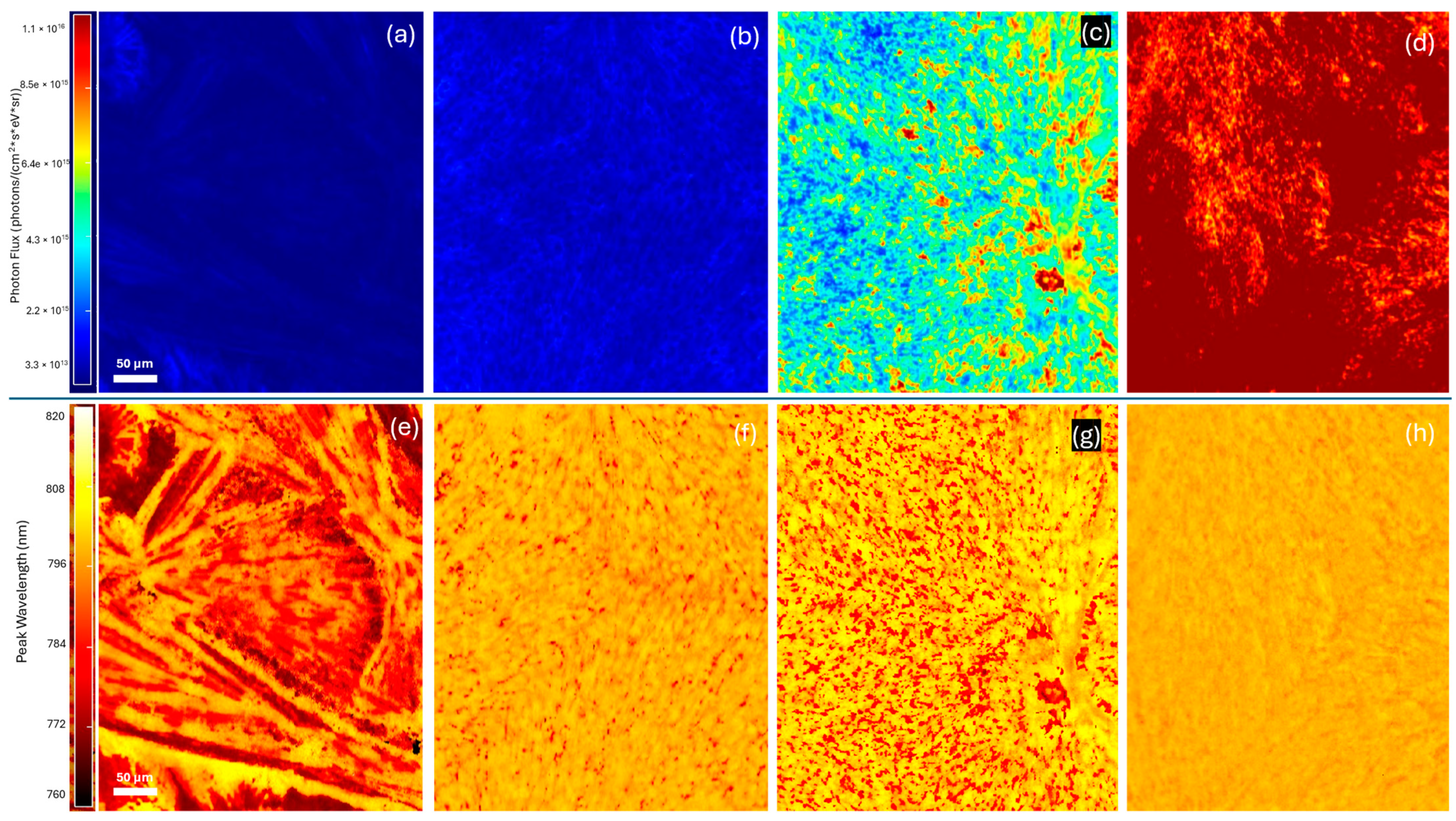
3. Results and Discussion

Perovskite samples containing 0%, 5%, 10%, and 20% weight concentrations of corn starch added directly to the precursor ink were tested. These values were selected based on previous work that demonstrated PSCs that retained high device PCE [40]. From Figure 2, the control (0 wt%) blade-coated MAPI film exhibited a relatively low Gc of 1.2 ± 0.4 J/m2, which is comparable with other reports of perovskite fracture energy [3,41]. MAPI with 5 wt% starch concentration showed low fracture energy as well, with a value of 1.95 ± 1.3 J/m2. The 10 wt% and 20 wt% starch concentration samples displayed significantly higher fracture energies with 9.19 ± 2.4 J/m2 and 10.6 ± 4.6 J/m2 values, respectively. There appears to be a threshold starch concentration above which the films are mechanically robust (~10 J/m2) at 10 wt% concentration. The 10 wt% and 20 wt% starch perovskites exceed the manufacturability threshold of 5 J/m2, a rule-of-thumb value that enables mechanical robustness of perovskite material against cracking and thin film stresses during manufacturing and operation [42]. We speculate that this could be due to a critical amount of starch enabling increased deformability, modified microstructure, and ‘scaffolding’ to the perovskite structure [24]. The 10 and 20 wt% of starch resulted in a significant 10× improvement to the fracture energy of MAPI, breaching the 5 J/m2 manufacturability threshold and demonstrating starch as an effective path to long-term film durability.
The addition of starch made thicker films potentially suitable for other energy detection applications as measured by profilometry after processing (Figure S1). Unmodified blade-coated MAPI had a thin film thickness of ~2.25 µm. The increasing addition of starch also increased the thickness. The 5 wt% starch sample had a thickness of 3.75 µm, the 10 wt% had a thickness of 8.75 µm, and the 20 wt% had a thickness of 10.5 µm (Figure 3). The 10 and 20 wt% samples thus resulted in both a more durable and substantially thicker film. The increase in film thickness is not necessarily the only reason behind the improvement in mechanical robustness. A previous study had shown that increased fracture energy could occur with thickness changes that are much lower when starch-MAPI films are spin-coated. Spin-coated MAPI films with starch contents of 10 wt% and 20 wt% were previously found to have a thickness of 450 nm and 1.5 µm, respectively [24]. While the blade-coated thickness of MAPI films with 10 wt% and 20 wt% starch had thicknesses of 8.75 µm and 10.5 µm.
The thickness of these blade-coated films is critical to their application, as the films with starch are by far too thick to ideally be used in solar applications [43,44,45]. A thicker perovskite film can result in the charge carriers recombining before extraction from the device and conversion into a current due to a carrier diffusion length shorter than a micron (nonradiative recombination) [46]. However, thicker perovskite films do have potential applications for high energy detection due to a thicker active layer with higher absorption length [31,32,33,34]. A previous study found that blade-coated MAPI with a thickness of 16.5 µm served as a functioning self-powered X-ray detector under an irradiation dose rate of 0.2372 mGyairs−1 [47]. Other research found that for optimal X-ray photoconductivity, MAPI films should have a thickness of ∼30 μm when used for a conventional CuKα X-ray tube source (8 keV) [48]. In general, film thicknesses must be equal to or higher than the X-ray absorption length selected. These thicker MAPI films may also be suitable for alpha particle detection, as alpha particles are heavy and have a much shorter penetration depth compared to X-rays. The technique displayed here is highly versatile as it offers the ability to control the thickness of films over 10µm, which can ideally be used in low-energy X-ray detection applications.
To better understand the effect that starch has on the composition of the film cross-section along with its distribution throughout the film, Glow Discharge Optical Emission Spectroscopy (GDOES) was used [49,50]. GDOES obtained the elemental composition of samples with 5–20 wt% starch. GDOES profiled through the thickness of the sample, sputtering through the perovskite film with cornstarch (C6H10O5) to the glass substrate (as indicated by sodium, Na) (Figure 4). The control and 5 wt% starch concentration samples reached the substrate, as evidenced by the increase in Na more quickly than the 10 wt% and 20 wt%. This increase in Na more quickly is due to the higher thicknesses that the 10 wt% and 20 wt% films have (Figure 3). Furthermore, the control and 5 wt% starch concentration samples had decreasing carbon compositions, while the 10 wt% and 20 wt% starch had stable or increasing carbon compositions. Carbon becomes more evenly dispersed and uniform throughout the sample as starch content increases. This is suggestive that the starch is incorporated throughout each sample. Interestingly, the oxygen signal is not as uniformly distributed, and it shows a larger concentration near the buried interface with the glass for the 10 wt% and 20 wt% starch concentrations. Since oxygen is also a component of the starch, this suggests that there could be a slightly higher presence near the bottom of the film. The increased amount of carbon—indicating the presence of starch—is hypothesized to reinforce the perovskite microstructure and enable higher Gc values.
X-ray diffraction was used to study the effect of starch on the residual perovskite film stress after processing using the sin2ψ method (Figure S2a–d). Without any starch, the 0 wt% showed a tensile film stress of 27 MPa. Residual tensile stress is expected and widely reported after processing, as perovskites have a much higher thermal expansion coefficient than glass [37]. Compressive stresses were observed with 5 wt% and higher concentrations of starch additive (Figure 5). The 5 wt% starch resulted in the largest compressive stress at −65 MPa. Additionally, this behavior agrees with previous work that found that the addition of gellan gum and starch polymers induced compressive stresses and translated to blade-coated perovskites [7]. Interestingly, the compressive stress induced by the additive was found to be lower in magnitude with higher starch additive concentration. The 10 wt% and 20 wt% starch additions exhibited slightly less compressive stresses at −46 and −41 MPa, respectively. This effect could be due to the substantial increase in film thickness, which generates internal stress that can offset some of the compressive stress from processing. Compressive stresses within the perovskite are beneficial to the film due to the increased stability and potential healing properties they impart on structural defects [51].
Optoelectronic properties were studied using hyperspectral photoluminescence to map the effect of starch on the emission of MAPI films. From Figure 6, the photoluminescence intensity of the samples at 760 nm increased with starch concentration from ~1013 photons/(cm2·s·eV·sr) without starch (Figure 6a) to ~1014 photons/(cm2·s·eV·sr) with 5 wt% (Figure 6b) to ~1015 photons/(cm2·s·eV·sr) with 10 wt% and ~1016 photons/(cm2·s·eV·sr) with 20 wt% (Figure 6d). From 0 wt% to 20 wt% starch, there was about three orders of magnitude increase in photoluminescence intensity. This observed higher photoluminescence intensity is expected and likely due in part to increased thickness due to the starch. The effect starch has on improving photoluminescence intensity indicates higher built-in voltage, an effect that correlates to the VOC (open circuit voltage) in a device. Photoluminescence intensity offers insight into the photoexcited charge–carrier density, which corresponds to the magnitude of the VOC in a device [52]. Here, the photoluminescence is seen to improve with the addition of starch, suggesting that starch may be able to improve the VOC of a photovoltaic device. This conclusion agrees with previous work that observed a PCE of 18.8% with 10 wt% of starch additive [24].
The hyperspectral images also offer insight into the morphology of the films with starch. The inclusion of starch aids in the uniformity of the peak wavelength at which the film is most luminescent (Figures S3–S6). Specifically, the 0 wt% starch has a variation in emission peak that varies by 42 nm, as seen in Figure 6e. Starch addition at 5 wt% had a range of 17 nm (Figure 6f), while 10 wt% had a wavelength emission range of 25 nm (Figure 6g). This variation in emission reduced to 5 nm in the 20 wt% starch film as seen across image Figure 6h. Altogether, the addition of the starch additive resulted in more compact and uniform morphology as well as more uniform wavelength peak emission—suggestive of a more homogeneous film and correlating directly with morphology improvements from the starch addition—than unmodified MAPI. The addition of starch shows better film morphology, suggesting that there are fewer defects in the film, which is also seen to correlate to optimal optoelectronic performance and structural improvement relating to mechanical robustness.
The experiments conducted in this study have shown that starch additive effectively aids in film stability while creating a mechanically robust film. The starch’s beneficial behavior is comparable to that of the biopolymer additive, gellan gum. Previous work has found that 0.56 wt% of gellan gum resulted in a similar fracture energy of 10.9 J/m2 [53]. Interestingly, when compared to gellan gum, blade-coated MAPI films with starch have significantly higher thicknesses. Earlier work has shown that blade-coated films with 0.56 wt% gellan gum had a thickness of 200 nm, while the work in this study found that 5 wt% of starch resulted in a film thickness of 3.75 µm [7]. Gellan gum was also seen to similarly improve the photoluminescence intensity of MAPI films. Other work has shown that biopolymer additives can also reduce phase segregation in mixed halide perovskites [54]. In comparison to other additives, starch has been shown to effectively thicken and improve the morphology of MAPI films, making this method particularly advantageous for applications that require thicker active layers. This study offers an advantage in using scalable, single-step, open-air processing to improve fracture energy of perovskite films while simultaneously adjusting morphology and thickness over a wide range for X-ray, alpha, and beta particle detection applications.
Based on the ability to create high-quality films greater than 10 µm thick, further investigations should be conducted on the practical high-energy detection applications of perovskite with starch additives. In particular, it will be necessary to investigate the potential effects of X-rays on the starch within the MAPI films. It could be worthwhile to investigate high-detection applications with other additives as well. For instance, there is the opportunity to utilize additives such as gellan gum, which results in a thicker film with less weight concentration added due to its higher viscosity [7]. Comparative high-energy detection studies of perovskites with various additives could offer further insight into the development of a tunable, durable, and scalable perovskite film. Importantly, a key question remains of the resistance that biopolymer additives will offer against high-energy sources, as organic materials typically are more readily decomposed. There is an opportunity to use fully inorganic perovskite compositions (Cs in place of MA as the A-site) and to perform a sintering or solvent removal step of the additive, but the effect this will have on the mechanical robustness and morphology remains unknown [55].

4. Conclusions

This work elaborates on the mechanism behind and implications of improved fracture energy from starch additives in metal halide perovskite films. The key result is that starch concentrations of 10 wt% and above result in a ~10× increase in fracture energy, and changes in structural and elemental properties can be used to explain this improvement. The starch acts as reinforcement to the perovskite based on its uniform distribution throughout the film. It also acts as a thickener of the film, where 10 wt% starch resulted in a ~4× thicker film than plain MAPI. Starch was further observed to induce desirable compressive film stresses within the perovskite, indicating higher mechanical stability, especially due to the simultaneous increase in fracture energy. The use of starch was also seen to enhance the uniformity and photon flux from hyperspectral photoluminescence measurements of the perovskite. Overall, the processes used in this study offer a strategy to create a tunable, open-air, and scalable strategy to make durable perovskite films.

Supplementary Materials

The following supporting information can be downloaded at: https://www.mdpi.com/article/10.3390/pr12091901/s1, Figure S1: Tencor P-16 Profilometer images of MAPI samples with starch additive ranging from 0 wt% to 20 wt%; Figure S2: XRD sin2ψ method raw data graphs displaying d-spacing (dϕψ) vs. [(1 + ν)∗sin2ψ − 2ν]/E for MAPI samples with starch additive ranging from 0 wt% to 20 wt%; Figure S3: Wavelength variation of hyperspectral image of plain MAPI; Figure S4: Wavelength variation of hyperspectral image of MAPI with 5 wt% of starch additive; Figure S5: Wavelength variation of hyperspectral image of MAPI with 10 wt% of starch additive; Figure S6: Wavelength variation of hyperspectral image of MAPI with 20 wt% of starch additive.

Author Contributions

Conceptualization: K.B. and N.R.; Funding Acquisition: N.R.; Methodology: N.R. and K.B.; Validation: M.L., M.A. and M.M.; Formal Analysis: K.B. and M.M.; Investigation: K.B., M.A. and M.M.; Resources: N.R.; Writing-original draft preparation: K.B.; Writing-reviewing and editing: M.A., M.L., M.M. and N.R.; Visualization: K.B.; Supervision: N.R.; Project Administration: N.R. All authors have read and agreed to the published version of the manuscript.

Funding

This material is based upon work supported by the National Science Foundation under Grant No. 2339233. The authors also acknowledge the use of facilities within the Eyring Materials Center at Arizona State University, supported in part by NNCI-ECCS-1542160.

Data Availability Statement

Data will be made available upon reasonable request.

Acknowledgments

The authors acknowledge resources and support from the Advanced Electronics and Photonics Core Facility at Arizona State University.

Conflicts of Interest

The authors have no conflicts of interest to report.

References

  1. Dai, Z.; Padture, N.P. Challenges and Opportunities for the Mechanical Reliability of Metal Halide Perovskites and Photovoltaics. Nat. Energy 2023, 8, 1319–1327. [Google Scholar] [CrossRef]
  2. Dai, Z.; Doyle, M.C.; Liu, X.; Hu, M.; Wang, Q.; Athanasiou, C.E.; Liu, Y.; Sheldon, B.W.; Gao, H.; Liu, S.; et al. The Mechanical Behavior of Metal-Halide Perovskites: Elasticity, Plasticity, Fracture, and Creep. Scr. Mater. 2023, 223, 115064. [Google Scholar] [CrossRef]
  3. Dai, Z.; Yadavalli, S.K.; Hu, M.; Chen, M.; Zhou, Y.; Padture, N.P. Effect of Grain Size on the Fracture Behavior of Organic-Inorganic Halide Perovskite Thin Films for Solar Cells. Scr. Mater. 2020, 185, 47–50. [Google Scholar] [CrossRef]
  4. Li, M.; Johnson, S.; Gil-Escrig, L.; Sohmer, M.; Figueroa Morales, C.A.; Kim, H.; Sidhik, S.; Mohite, A.; Gong, X.; Etgar, L.; et al. Strategies to Improve the Mechanical Robustness of Metal Halide Perovskite Solar Cells. Energy Adv. 2023, 3, 273–280. [Google Scholar] [CrossRef]
  5. Seong, S.; Liu, Y.; Gong, X. Mechanical Study of Perovskite Solar Cells: Opportunities and Challenges for Wearable Power Source. Opt. Mater. Express 2022, 12, 772. [Google Scholar] [CrossRef]
  6. McAndrews, G.R.; Guo, B.; Morales, D.A.; Amassian, A.; McGehee, M.D. How the Dynamics of Attachment to the Substrate Influence Stress in Metal Halide Perovskites. APL Energy 2023, 1, 036110. [Google Scholar] [CrossRef]
  7. Ahmad, M.; Cartledge, C.; McAndrews, G.; Giuri, A.; McGehee, M.D.; Rizzo, A.; Rolston, N. Tuning Film Stresses for Open-Air Processing of Stable Metal Halide Perovskites. ACS Appl. Mater. Interfaces 2023, 15, 51117–51125. [Google Scholar] [CrossRef]
  8. Yadavalli, S.K.; Chen, M.; Hu, M.; Dai, Z.; Zhou, Y.; Padture, N.P. Electron-Beam-Induced Cracking in Organic-Inorganic Halide Perovskite Thin Films. Scr. Mater. 2020, 187, 88–92. [Google Scholar] [CrossRef]
  9. Ramirez, C.; Yadavalli, S.K.; Garces, H.F.; Zhou, Y.; Padture, N.P. Thermo-Mechanical Behavior of Organic-Inorganic Halide Perovskites for Solar Cells. Scr. Mater. 2018, 150, 36–41. [Google Scholar] [CrossRef]
  10. Rolston, N.; Scheideler, W.J.; Flick, A.C.; Chen, J.P.; Elmaraghi, H.; Sleugh, A.; Zhao, O.; Woodhouse, M.; Dauskardt, R.H. Rapid Open-Air Fabrication of Perovskite Solar Modules. Joule 2020, 4, 2675–2692. [Google Scholar] [CrossRef]
  11. Kojima, A.; Teshima, K.; Shirai, Y.; Miyasaka, T. Organometal Halide Perovskites as Visible-Light Sensitizers for Photovoltaic Cells. J. Am. Chem. Soc. 2009, 131, 6050–6051. [Google Scholar] [CrossRef]
  12. Yoo, J.J.; Seo, G.; Chua, M.R.; Park, T.G.; Lu, Y.; Rotermund, F.; Kim, Y.K.; Moon, C.S.; Jeon, N.J.; Correa-Baena, J.P.; et al. Efficient Perovskite Solar Cells via Improved Carrier Management. Nature 2021, 590, 587–593. [Google Scholar] [CrossRef] [PubMed]
  13. Min, H.; Lee, D.Y.; Kim, J.; Kim, G.; Lee, K.S.; Kim, J.; Paik, M.J.; Kim, Y.K.; Kim, K.S.; Kim, M.G.; et al. Perovskite Solar Cells with Atomically Coherent Interlayers on SnO2 Electrodes. Nature 2021, 598, 444–450. [Google Scholar] [CrossRef] [PubMed]
  14. Lin, R.; Xu, J.; Wei, M.; Wang, Y.; Qin, Z.; Liu, Z.; Wu, J.; Xiao, K.; Chen, B.; Park, S.M.; et al. All-Perovskite Tandem Solar Cells with Improved Grain Surface Passivation. Nature 2022, 603, 73–78. [Google Scholar] [CrossRef] [PubMed]
  15. Peters, I.M.; Hauch, J.; Brabec, C.; Sinha, P. The Value of Stability in Photovoltaics. Joule 2021, 5, 3137–3153. [Google Scholar] [CrossRef]
  16. Yan, J.; Savenije, T.J.; Mazzarella, L.; Isabella, O. Progress and Challenges on Scaling up of Perovskite Solar Cell Technology. Sustain. Energy Fuels 2022, 6, 243–266. [Google Scholar] [CrossRef]
  17. Deokate, R. Spin Coating/Doctor-Blading/Self-Assembly of Metal Oxide Nanostructures. In Solution Methods for Metal Oxide Nanostructures; Elsevier: Amsterdam, The Netherlands, 2023. [Google Scholar]
  18. Srivastava, A.; Satrughna, J.A.K.; Tiwari, M.K.; Kanwade, A.; Yadav, S.C.; Bala, K.; Shirage, P.M. Lead Metal Halide Perovskite Solar Cells: Fabrication, Advancement Strategies, Alternatives, and Future Perspectives. Mater. Today Commun. 2023, 35, 105686. [Google Scholar] [CrossRef]
  19. Jiao, J.; Yang, C.; Wang, Z.; Yan, C.; Fang, C. Solvent Engineering for the Formation of High-Quality Perovskite Films: A Review. Results Eng. 2023, 18, 101158. [Google Scholar] [CrossRef]
  20. Geistert, K.; Ternes, S.; Ritzer, D.B.; Paetzold, U.W. Controlling Thin Film Morphology Formation during Gas Quenching of Slot-Die Coated Perovskite Solar Modules. ACS Appl. Mater. Interfaces 2023, 15, 52519–52529. [Google Scholar] [CrossRef]
  21. Fievez, M.; Singh Rana, P.J.; Koh, T.M.; Manceau, M.; Lew, J.H.; Jamaludin, N.F.; Ghosh, B.; Bruno, A.; Cros, S.; Berson, S.; et al. Slot-Die Coated Methylammonium-Free Perovskite Solar Cells with 18% Efficiency. Sol. Energy Mater. Sol. Cells 2021, 230, 111189. [Google Scholar] [CrossRef]
  22. Vesce, L.; Stefanelli, M.; Rossi, F.; Castriotta, L.A.; Basosi, R.; Parisi, M.L.; Sinicropi, A.; Di Carlo, A. Perovskite Solar Cell Technology Scaling-up: Eco-Efficient and Industrially Compatible Sub-Module Manufacturing by Fully Ambient Air Slot-Die/Blade Meniscus Coating. Prog. Photovolt. Res. Appl. 2024, 32, 115–129. [Google Scholar] [CrossRef]
  23. Shen, D.; Luo, C.; Zheng, R.; Li, Q.; Chen, Y. Improvement of Photoluminescence Intensity and Film Morphology of Perovskite by Ionic Liquids Additive. In Proceedings of the E3S Web of Conferences, Hyderabad, India, 24–26 September 2021; EDP Sciences: Les Ulis, France, 2021; Volume 257. [Google Scholar]
  24. Giuri, A.; Rolston, N.; Colella, S.; Listorti, A.; Esposito Corcione, C.; Elmaraghi, H.; Lauciello, S.; Dauskardt, R.H.; Rizzo, A. Robust, High-Performing Maize-Perovskite-Based Solar Cells with Improved Stability. ACS Appl. Energy Mater. 2021, 4, 11194–11203. [Google Scholar] [CrossRef] [PubMed]
  25. Hamukwaya, S.L.; Hao, H.; Zhao, Z.; Dong, J.; Zhong, T.; Xing, J.; Hao, L.; Mashingaidze, M.M. A Review of Recent Developments in Preparation Methods for Large-Area Perovskite Solar Cells. Coatings 2022, 12, 252. [Google Scholar] [CrossRef]
  26. Sun, W.; Choy, K.L.; Wang, M. The Role of Thickness Control and Interface Modification in Assembling Efficient Planar Perovskite Solar Cells. Molecules 2019, 24, 3466. [Google Scholar] [CrossRef]
  27. Park, J.Y.; Song, R.; Liang, J.; Jin, L.; Wang, K.; Li, S.; Shi, E.; Gao, Y.; Zeller, M.; Teat, S.J.; et al. Thickness Control of Organic Semiconductor-Incorporated Perovskites. Nat. Chem. 2023, 15, 1745–1753. [Google Scholar] [CrossRef] [PubMed]
  28. Liu, D.; Li, Y.; Shi, B.; Yao, X.; Fan, L.; Zhao, S.; Liang, J.; Ding, Y.; Wei, C.; Zhang, D.; et al. Tailoring Morphology and Thickness of Perovskite Layer for Flexible Perovskite Solar Cells on Plastics: The Role of CH3NH3I Concentration. Sol. Energy 2017, 147, 222–227. [Google Scholar] [CrossRef]
  29. Liu, Y.; Gao, C.; Li, D.; Zhang, X.; Zhu, J.; Wu, M.; Liu, W.; Shi, T.; He, X.; Wang, J.; et al. Dynamic X-Ray Imaging with Screen-Printed Perovskite CMOS Array. Nat. Commun. 2024, 15, 1588. [Google Scholar] [CrossRef]
  30. Kakavelakis, G.; Gedda, M.; Panagiotopoulos, A.; Kymakis, E.; Anthopoulos, T.D.; Petridis, K. Metal Halide Perovskites for High-Energy Radiation Detection. Adv. Sci. 2020, 7, 2002098. [Google Scholar] [CrossRef]
  31. Huang, K.W.; Li, M.H.; Chen, Y.T.; Wen, Z.X.; Lin, C.F.; Chen, P. Fast Fabrication of Μm-Thick Perovskite Films by Using a One-Step Doctor-Blade Coating Method for Direct X-Ray Detectors. J. Mater. Chem. C Mater. 2023, 12, 1533–1542. [Google Scholar] [CrossRef]
  32. Atkinson, N.J.; Evans, J.; Simmonds, D.J. Material Change for X-ray Detectors; Macmillan Publishers Limited: New York, NY, USA, 2014; Volume 42. [Google Scholar]
  33. Li, G.; Zhao, C.; Liu, Y.; Ren, J.; Zhang, Z.; Di, H.; Jiang, W.; Mei, J.; Zhao, Y. High-Performance Perovskite Betavoltaics Employing High-Crystallinity MAPbBr3Films. ACS Omega 2021, 6, 20015–20025. [Google Scholar] [CrossRef]
  34. Kim, Y.C.; Kim, K.H.; Son, D.Y.; Jeong, D.N.; Seo, J.Y.; Choi, Y.S.; Han, I.T.; Lee, S.Y.; Park, N.G. Printable Organometallic Perovskite Enables Large-Area, Low-Dose X-Ray Imaging. Nature 2017, 550, 87–91. [Google Scholar] [CrossRef] [PubMed]
  35. Romano, V.; Agresti, A.; Verduci, R.; D’Angelo, G. Advances in Perovskites for Photovoltaic Applications in Space. ACS Energy Lett. 2022, 7, 2490–2514. [Google Scholar] [CrossRef] [PubMed]
  36. Lang, F.; Nickel, N.H.; Bundesmann, J.; Seidel, S.; Denker, A.; Albrecht, S.; Brus, V.V.; Rappich, J.; Rech, B.; Landi, G.; et al. Radiation Hardness and Self-Healing of Perovskite Solar Cells. Adv. Mater. 2016, 28, 8726–8731. [Google Scholar] [CrossRef]
  37. Dailey, M.; Li, Y.; Printz, A.D. Residual Film Stresses in Perovskite Solar Cells: Origins, Effects, and Mitigation Strategies. ACS Omega 2021, 6, 30214–30223. [Google Scholar] [CrossRef]
  38. Luo, Q.; Jones, A.H. High-Precision Determination of Residual Stress of Polycrystalline Coatings Using Optimised XRD-Sin2ψ Technique. Surf. Coat. Technol. 2010, 205, 1403–1408. [Google Scholar] [CrossRef]
  39. Photon, E. Leverage the Power of Hyperspectral Microscopy. Available online: https://www.photonetc.com/products/ima (accessed on 26 June 2024).
  40. Giuri, A.; Masi, S.; Listorti, A.; Gigli, G.; Colella, S.; Esposito Corcione, C.; Rizzo, A. Polymeric Rheology Modifier Allows Single-Step Coating of Perovskite Ink for Highly Efficient and Stable Solar Cells. Nano Energy 2018, 54, 400–408. [Google Scholar] [CrossRef]
  41. Rolston, N.; Printz, A.D.; Tracy, J.M.; Weerasinghe, H.C.; Vak, D.; Haur, L.J.; Priyadarshi, A.; Mathews, N.; Slotcavage, D.J.; McGehee, M.D.; et al. Effect of Cation Composition on the Mechanical Stability of Perovskite Solar Cells. Adv. Energy Mater. 2018, 8, 1702116. [Google Scholar] [CrossRef]
  42. Watson, B.L.; Rolston, N.; Printz, A.D.; Dauskardt, R.H. Scaffold-Reinforced Perovskite Compound Solar Cells. Energy Environ. Sci. 2017, 10, 2500–2508. [Google Scholar] [CrossRef]
  43. Ouslimane, T.; Et-taya, L.; Elmaimouni, L.; Benami, A. Impact of Absorber Layer Thickness, Defect Density, and Operating Temperature on the Performance of MAPbI3 Solar Cells Based on ZnO Electron Transporting Material. Heliyon 2021, 7, e06379. [Google Scholar] [CrossRef]
  44. Son, C.; Son, H.; Jeong, B.-S. Enhanced Conversion Efficiency in MAPbI3 Perovskite Solar Cells through Parameters Optimization via SCAPS-1D Simulation. Appl. Sci. 2024, 14, 2390. [Google Scholar] [CrossRef]
  45. Rai, M.; Wong, L.H.; Etgar, L. Effect of Perovskite Thickness on Electroluminescence and Solar Cell Conversion Efficiency. J. Phys. Chem. Lett. 2020, 11, 8189–8194. [Google Scholar] [CrossRef]
  46. Shi, P.; Xu, J.; Yavuz, I.; Huang, T.; Tan, S.; Zhao, K.; Zhang, X.; Tian, Y.; Wang, S.; Fan, W.; et al. Strain Regulates the Photovoltaic Performance of Thick-Film Perovskites. Nat. Commun. 2024, 15, 2579. [Google Scholar] [CrossRef]
  47. Tan, J.; Gao, X.; Huang, X.; Wangyang, P.; Sun, H.; Yang, D.; Zeng, T. Self-Powered X-Ray Detector Based on Lead Halide Perovskites under Electric Field Poling Effect. J. Mater. Sci. Mater. Electron. 2023, 34, 1199. [Google Scholar] [CrossRef]
  48. Yakunin, S.; Sytnyk, M.; Kriegner, D.; Shrestha, S.; Richter, M.; Matt, G.J.; Azimi, H.; Brabec, C.J.; Stangl, J.; Kovalenko, M.V.; et al. Detection of X-Ray Photons by Solution-Processed Lead Halide Perovskites. Nat. Photonics 2015, 9, 444–449. [Google Scholar] [CrossRef]
  49. Dally, P.; Messou, D.; Robillard, M.; Cacovich, S.; Yaiche, A.; Rousset, J.; Etcheberry, A.; Bouttemy, M. Probing the Chemistry of Perovskite Systems by XPS and GD-OES Depth-Profiling: Potentials and Limitations. In Proceedings of the Conference Record of the IEEE Photovoltaic Specialists Conference, Miami, FL, USA, 20–25 June 2021; Institute of Electrical and Electronics Engineers Inc.: New York, NY, USA, 2021; pp. 931–934. [Google Scholar]
  50. Zheng, D.; Volovitch, P.; Pauporté, T. What Can Glow Discharge Optical Emission Spectroscopy (GD-OES) Technique Tell Us about Perovskite Solar Cells? Small Methods 2022, 6, e2200633. [Google Scholar] [CrossRef]
  51. Rolston, N.; Bush, K.A.; Printz, A.D.; Gold-Parker, A.; Ding, Y.; Toney, M.F.; McGehee, M.D.; Dauskardt, R.H. Engineering Stress in Perovskite Solar Cells to Improve Stability. Adv. Energy Mater. 2018, 8, 1802139. [Google Scholar] [CrossRef]
  52. Goetz, K.P.; Taylor, A.D.; Paulus, F.; Vaynzof, Y. Shining Light on the Photoluminescence Properties of Metal Halide Perovskites. Adv Funct Mater 2020, 30, 1910004. [Google Scholar] [CrossRef]
  53. Cartledge, C.; Penukula, S.; Giuri, A.; Bakshi, K.; Ahmad, M.; Mahaffey, M.; Li, M.; Zhang, R.; Rizzo, A.; Rolston, N. Scalable and Quench-Free Processing of Metal Halide Perovskites in Ambient Conditions. Energies 2024, 17, 1455. [Google Scholar] [CrossRef]
  54. Bisconti, F.; Leoncini, M.; Bravetti, G.; Giuri, A.; Polimeno, L.; Carallo, S.; Colella, S.; Gatto, L.; Grandi, F.; Cinquanta, E.; et al. Blocking Wide Bandgap Mixed Halide Perovskites’ Decomposition through Polymer Inclusion. J. Mater. Chem. C Mater. 2023, 11, 12213–12221. [Google Scholar] [CrossRef]
  55. Zhao, X.; Liu, T.; Burlingame, Q.C.; Liu, T.; Holleyiii, R.; Cheng, G.; Yao, N.; Gao, F.; Loo, Y.-L. Accelerated Aging of All-Inorganic, Interface-Stabilized Perovskite Solar Cells. Science 2022, 377, 307–310. [Google Scholar] [CrossRef]
Figure 1. Schematics of methods used for sample fabrication and DCB testing. (a) Blade-coating technique used to deposit perovskite ink with starch. (b) Sample fabrication for DCB testing. (c) DCB crack path through fabricated sample.
Processes 12 01901 g001
Figure 2. Fracture energy (Gc) of MAPI with 0, 5, 10, and 20 wt% concentrations of starch.
Processes 12 01901 g002
Figure 3. Thickness of MAPI samples with starch additive in 0, 5, 10, and 20 wt% concentrations.
Processes 12 01901 g003
Figure 4. Glow Discharge Optical Electron Spectroscopy (GDOES) depth profiles of ambient blade-coated MAPI samples with 0, 5, 10, and 20 wt% concentrations of starch.
Processes 12 01901 g004
Figure 5. Thin film residual stress measurements from X-ray diffraction sin2ψ analysis of the 0, 5, 10, and 20 wt% MAPI-starch samples that were ambient blade-coated on glass. The colored squares represent the different starch concentrations; black being 0 wt%, red is 5 wt%, maroon is 10 wt%, and yellow is 20 wt%.
Processes 12 01901 g005
Figure 6. Hyperspectral photoluminescence images of the MAPI films that were ambient blade-coated on glass with starch additives. The top row (ad) has photoluminescence intensity profiles, and the bottom row (eh) has the wavelength profiles. The first columns (a,e) are of 0% starch, (b,f) are of 5% starch, (c,g) are of 10% starch, and (d,h) are of 20% starch. The field of view in all images is the same. In the top row of intensity profiles, higher starch concentrations (c,d) reached higher photoluminescence intensities. Higher starch concentrations were seen to cause more uniform wavelength profiles in (g,h) specifically.
Processes 12 01901 g006
Disclaimer/Publisher’s Note: The statements, opinions and data contained in all publications are solely those of the individual author(s) and contributor(s) and not of MDPI and/or the editor(s). MDPI and/or the editor(s) disclaim responsibility for any injury to people or property resulting from any ideas, methods, instructions or products referred to in the content.

