1. Introduction
Harvesting solar energy by photon absorption in metal nanostructures and the subsequent collection of photo-generated hot electrons via the processes of internal photo-emission has been actively explored as an alternative approach to traditional photovoltaics (PV), as well as for catalysis and photo-detection [
1,
2,
3,
4,
5,
6]. The energy of the absorbed photons raises the energy of electrons above the Fermi level in the absorber material, creating a population of energetic, or ‘hot’, electrons, whose energies are out of thermal equilibrium with the crystal lattice. Hot electrons typically cool down very fast due to scattering on cold electrons, lattice defects, and phonons. The cooling process occurs on the picosecond timescale in most metals [
2,
4,
7,
8,
9]. If, however, these hot electrons can be extracted before they cool down, they can generate voltage and/or current in the external circuit [
10].
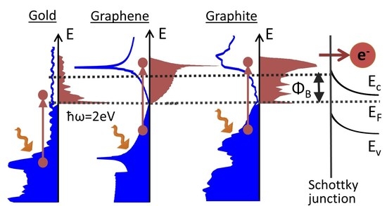
One possible hot electron extraction scheme is based on their injection above the Schottky barrier, which forms at the interface between a metal and a semiconductor (
Figure 1). In this scheme, hot electrons generated by the absorption of photons with energies below the semiconductor bandgap can still be harvested [
11,
12,
13]. This offers a way to potentially increase the conversion efficiency of PV cells and to extend the bandwidth of photo-detectors. Unlike conventional PV cells, which rely on minority-carrier transport in the semiconductor material, in Schottky devices the semiconductor is only used for the majority carrier transport and separation. The photo-generated hot electrons can also be used to drive catalytic reactions [
3,
4,
14].
Traditionally, plasmonic metals such as gold (Au) are considered as good material candidates for gapless photon absorbers, which are potentially capable of the full solar spectrum harvesting. Unfortunately, the photon-to-electricity energy conversion efficiencies in the hot-electron solar harvesting devices demonstrated to date have been extremely low [
15,
16,
17,
18]. The disappointing efficiency partially stems from the difficulty in achieving efficient and broadband light absorption in metal nanostructures. State-of-the-art approaches to improving photon energy harvesting typically focus on engineering the photon density of states to achieve perfect light absorption in various materials. The efficiency and bandwidth of noble-metal absorptance can be increased, although it often requires precise nano-patterning and/or external optical trapping schemes. However, it has been recently revealed that the number of energy states available for electron transitions in the absorber material imposes strict limitations on the upper limits of efficiency achievable in internal photo-emission (IPE) solar energy conversion platforms even if the perfect absorptance is achieved [
19,
20,
21,
22]. Accordingly, to select a good material candidate for a target spectral window, material properties beyond the ability to efficiently absorb photons should be considered. Another obvious limitation of gold and other noble metals is their high price stemming from the low abundance of these materials on our planet. To overcome this limitation, other cheaper metals such as, e.g., aluminum, copper, and silver, have been explored for applications in energy harvesting through hot electron generation [
8,
22,
23].
Semimetals, such as, e.g., carbon-based materials, lack an electronic bandgap, and can be used instead of metals for harvesting both visible and near-infrared photons. They can also form rectifying Schottky junctions with conventional semiconductor materials [
24,
25,
26,
27,
28], making them promising material candidates for IPE absorbers. In contrast to metals, which have a partially-filled conduction band, semimetals are characterized by an overlap between the bottom of the conduction band and the top of the valence band. Unlike other semimetals such as arsenic, antimony, bismuth, and α-tin, some forms of carbon are non-toxic, cheap, and abundantly present in the earth’s core. Here, we consider two forms of carbon: graphite, which is a typical semimetal, and a monolayer graphene, which is a semimetal with a negligible density of states at the Fermi level, and in which the energy is proportional to the momentum rather than its square. In the following, we use ab initio calculations of the electron density of states in the absorber material to evaluate the upper efficiency limits of IPE energy harvesting platforms. We used gold, graphite and graphene as sample material candidates to evaluate and compare using this approach, and demonstrate higher efficiency limits for the solar spectrum harvesting of sunlight potentially achievable with the use of graphite.
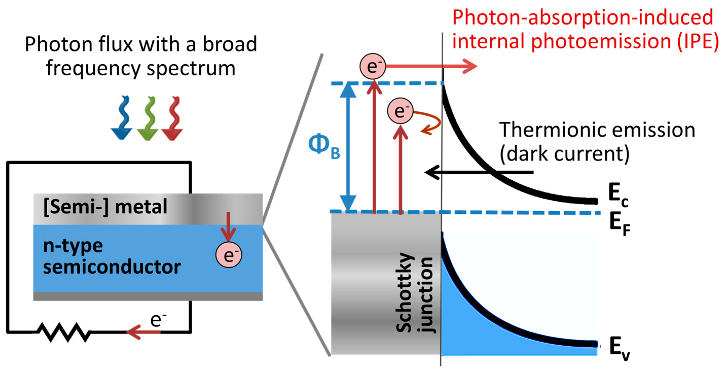
2. The Theory and Modeling of the Internal Photoemission Process
A schematic of a typical IPE device is shown in
Figure 1, and consists of a metal or semi-metal photon absorber, which forms a rectifying Schottky junction at an interface with a semiconductor [
29,
30,
31]. An electronic band diagram for the Schottky junction is shown in the right panel of
Figure 1 for the case of the junction between a metal and an n-type semiconductor. In the following, we limit the analysis to hot-electron-based IPE devices. However, the theory is fully applicable to the hot-hole-type IPE photon energy harvesters that utilize Schottky junctions between (semi-)metals and p-type semiconductors [
21,
32]. The electronic band gap in the semiconductor material forces the formation of the energy barrier of height
at the material interface, which only allows the transport of hot electrons from the metal to the semiconductor with energies at least
above the Fermi level
, as shown in
Figure 1. The height of the Schottky barrier depends on a combination of the metal and semiconductor materials, and typically varies in the 0.5–1.5 eV range [
24,
26,
31,
33]. Once these hot electrons are injected into the semiconductor, the band gap prevents their recombination with holes and preserves their extra energy in excess of the Fermi level. While the non-equilibrium IPE process drives the forward current through the Schottky junction, the equilibrium thermionic emission from the semiconductor into the (semi-)metal results in the reverse dark current, which reduces the efficiency of the IPE photon-energy-harvesting platforms.
The principle of operation of the IPE device is based on the three-step process, involving (1) hot carrier generation by a combination of direct photon absorption and an indirect absorption via plasmon excitation and subsequent decay; (2) hot carrier transport to the interface; and (3) their injection into the semiconductor material [
19,
20,
21,
34]. The two latter processes must compete with the hot carrier thermalization between themselves and with the lattice, which may reduce the IPE yield. For many decades, the semi-classical Fowler theory provided the analytical tool to evaluate the IPE yield. This theory is based on the spherical Fermi surface approximation for electrons in metals and the assumption that the kinetic energy of electrons
normal to the barrier must exceed the barrier height. The above assumptions result in the prediction of a small angular escape cone for electrons, whose angular width is limited by the cut-off value of the hot electron momentum normal to the interface [
35]. However, recent studies have shown that the IPE device performance can significantly exceed the limits predicted by the Fowler equation [
7,
20,
34,
36]. The observed differences were mostly attributed to the deviation from the escape-cone limitation, with the extra momentum provided via electron–phonon scattering, plasmon-to-hot-electron decay, and surface roughness of the material interfaces [
20,
34]. These observations are in line with prior work on super-lattice thermoelectric devices, where the increased number of hot electrons participating in the conduction process was attributed to the non-conservation of lateral momentum during the interface emission process [
37,
38]. The hot electron yield increase becomes especially pronounced in the case of absorbers fully embedded within a semiconductor and with at least one dimension smaller that the electron mean free path limited by the electron–electron scattering [
20,
34,
39]. Electron–phonon scattering increases the yield by changing the momentum of the non-equilibrium electrons and re-directing them into the escape cone without significant energy loss [
40]. The above factors increase the probability of the hot electron reaching the interface and escaping into the semiconductor.
Some recent studies of the IPE devices employed a simple band model—parabolic band approximation—for the electronic band structure of noble metal absorbers [
19,
20]. However, such approximation fails to correctly predict the IPE efficiency limits for materials with non-parabolic bands [
21,
23,
32], nano-scale absorbers exhibiting electron level quantization effects [
7], and absorbers under a broadband light illumination, which causes both inter-band and intra-band photon absorption [
21]. As such, the electronic band structure of the absorber material emerges as an important parameter that can either suppress or enhance the IPE yield in the Schottky-junction-type devices. The density of filled and empty electron states in the absorber material, which are available for the photon-induced upward electron transitions, strongly affects the first step of the IPE process, and thus establishes the absolute upper limit to the IPE device efficiency.
In the following, we use the density functional theory (DFT) to calculate the available density of electron states in the absorber material and to illustrate its effect on the upper efficiency limit of IPE devices. We use the DFT to calculate the electron band structure in gold and carbon materials, and predict significant differences in their upper efficiency limit estimates imposed by the materials’ electronic band structures. The electronic band structures of graphene and graphite offer potential performance improvement of IPE devices for either full or partial solar spectrum harvesting.
3. Band-Structure-Imposed Upper Limits of IPE Efficiency: Gold versus Carbon
We calculate the upper limit of the IPE light-to-current conversion efficiency under the assumptions of (i) perfect photon absorption across the whole solar spectrum; (ii) ballistic hot electron transport to the Schottky junction between the (semi-)metal and the semiconductor; and (iii) momentum matching of the hot electrons that makes possible their transport through the potential barrier (i.e., no escape cone limitation) [
19,
20,
21]. The short circuit current generated by light absorption in a Schottky device with the potential barrier of height
can be calculated as follows:
Here,
is the electron charge,
is the reduced Planck’s constant,
is the energy of photon,
is the incoming photon spectral flux, and
is the spectral photon absorptance. The IPE efficiency
is calculated as the probability of the photo-generated electron being injected across the potential barrier (see below). For solar harvesting applications,
, where
is the AM1.5D (ASTM G173-03) terrestrial solar spectrum [
41], and
is the solar concentration. Perfect absorptance condition yields
across the solar spectrum frequency range.
Under the ideal conditions for the ballistic electron transport and momentum non-conserved interface transport—i.e., considering the initial non-equilibrium distribution of hot electrons and assuming that all electrons with the energies higher than the barrier will transmit through the interface—the upper limiting value for
is solely determined by the IPE efficiency
. IPE efficiency characterizes the fraction of hot electrons that are generated by the absorption of light with frequency
, which have enough energy to be injected from the (semi-)metal into the semiconductor above the Schottky barrier [
19,
21]. IPE efficiency strongly depends on the electron band structure of the material, the absorbed photon energy, and the potential barrier height
It can be calculated as a ratio of the population of the hot electrons with sufficient energy to be emitted over the Schottky barrier to the total photo-excited electron population:
The population of photo-excited electrons in a given material is determined by its joint density of states, which depends on the number of initial
and final
electronic states available for upward transitions driven by photon absorption:
Here, is the Fermi–Dirac distribution function, which defines the probability of the energy level to be occupied at a the initial equilibrium lattice temperature, while defines the probability of the energy level being empty and available for the upward electron transition in the process of photo-excitation, is the Boltzmann constant, and is the lattice temperature.
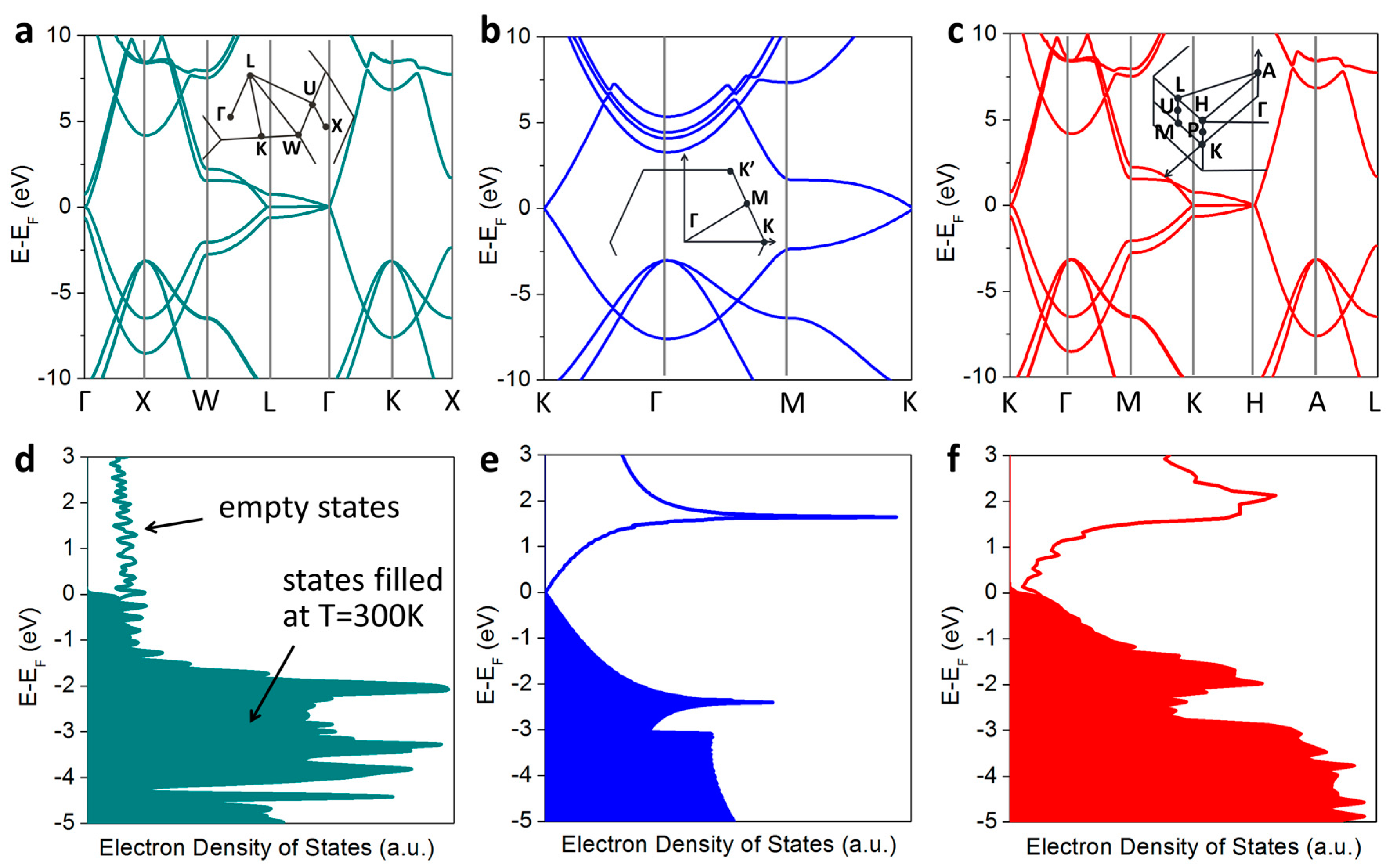
We calculated the electron band structure and the density of available electron states via the Density Functional Theory (DFT) simulations with the QUANTUM ESPRESSO package [
42]. We used the local density approximation (LDA) of Perdew and Zunger [
43] for all the materials examined, including gold, graphene and graphite. The projector augmented wave method [
44] was used for gold, while the pseudopotential given by Hartwigsen–Goedecker–Hutter [
45] was applied to graphite and graphene. Spin-orbit coupling in a scalar-relativistic level was also included for gold. Atomic coordinates in all cases were relaxed until the minimum force was below
. Electron band structures of the three materials are shown in
Figure 2a–c. The electron band energies were subsequently interpolated onto a much finer mesh using the tetrahedra method [
46] to calculate the electron density of states for the three materials shown in
Figure 2d–f. Detailed parameters used for each material are given in
Table 1.
In
Figure 2d–f, we show the population of electron states filled at room temperature (
filled curves) and the density of electron states available for the upward electron transitions in all the three materials considered. As can be seen in
Figure 2, the electron density of states calculated with the ab-initio DFT simulations deviates significantly from the parabolic band approximation used in some previous works [
19,
20]. Instead, electron densities of states for different materials exhibit complex energy distributions that peak at different energies relative to the Fermi level in the material.
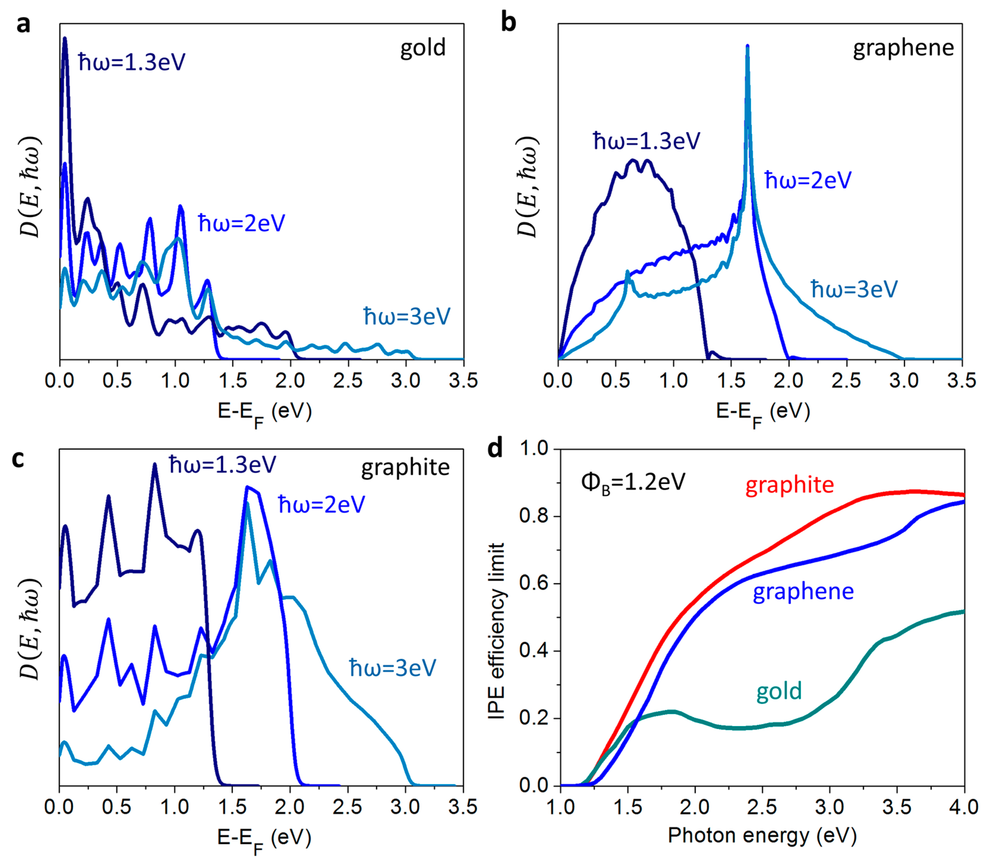
Figure 3a–c compare the joint density of states (
) calculated by using Equation (3) for the photon energy at the peak of the solar radiation
(blue lines) as well as for two other energies within the solar spectrum,
(navy lines) and
(light blue lines) for gold (a), graphene (b), and graphite (c). In Au, the population of hot electrons is dominated by the photo-induced transitions from the
d-bands, which results in the creation of many ‘lukewarm’ electrons with energies just above the Fermi level (
Figure 3a). Since only hot electrons with energies higher than the Schottky barrier height can be internally emitted into the semiconductor, the photo-excited hot electron population in Au yields low IPE efficiency. The joint densities of states of two carbon materials both exhibit peaks at higher hot electron energies (
Figure 3b,c), with a larger portion of hot electrons occupying higher-energy final states created in graphite than in graphene. Assuming that only hot electrons with energy higher than the barrier height can be internally emitted into the semiconductor over the barrier with a non-negligible probability, we used Equation (2) to calculate the limiting IPE efficiency as a function of the photon energy and barrier height. This efficiency is plotted in
Figure 3d as a function of the energy of absorbed photons for all the three materials for a fixed barrier height
. The data in
Figure 3d predict the highest IPE efficiencies for graphite at all frequencies of the solar spectrum, leading to the conclusion that the electron density of states in graphite is most favorable for achieving high IPE efficiency among the three materials considered.
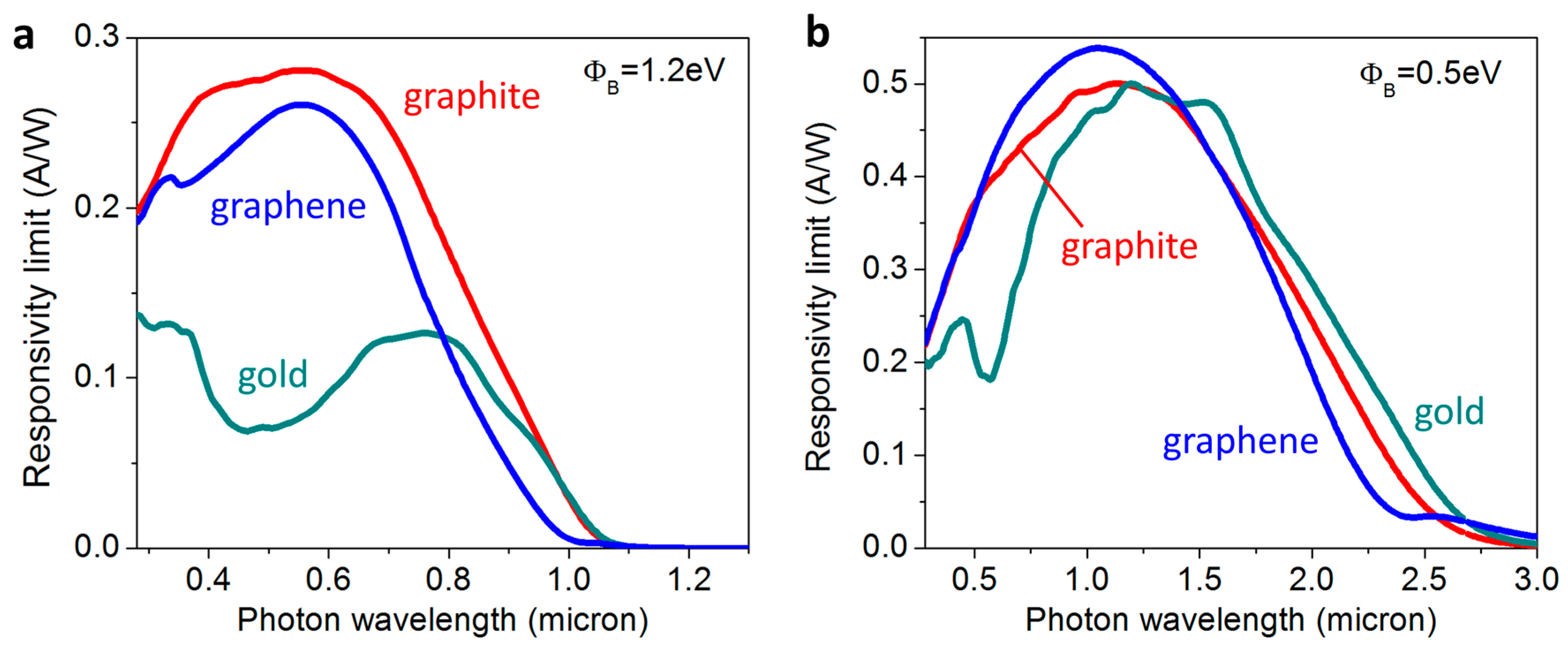
By substituting the data in
Figure 3 to Equation (1), we can now calculate the responsivity limit of the IPE photodetectors with different absorber materials as the ratios of their photo-generated short-circuit currents at zero applied voltage per watt of incident radiant power. This limit is plotted in
Figure 4 as a function of the incoming photon wavelength for two different Schottky barrier heights of 1.2 eV and 0.5 eV, respectively. Once again, we can observe the strong effect of the absorber material electron density of states on the IPE device responsivity limit, with carbon materials out-performing gold across the whole visible spectrum for any potential barrier height. The Au device responsivity limit approaches those for carbon-based IPE devices in the near-infrared (IR) range, and may even exceed them in the case of low-height potential barrier (
Figure 4b).
However, the photo-generated current that can be delivered to the external load is reduced by the reverse dark current due to thermionic emission through the Schottky barrier from the semiconductor into the (semi-)metal. Total current is defined trough the standard Schottky diode equation as follows:
where
is the applied voltage and
is the Boltzmann constant. The thermionic emission reverse current scales inverse exponentially with the potential barrier height, as the second power with the temperature, and depends on the specifics of the material interface through the modified Richardson constant
. In the following calculations, we used the Richardson constant value for titanium dioxide (
), which was previously reported in the literature [
47]. Titanium dioxide (TiO
2) is a common choice for semiconductors used in IPE devices [
6].
We define the overall limiting efficiency of the IPE solar energy converter as the ratio of the maximum electrical power delivered to the load to the total power of the incoming sunlight, i.e.,:
The maximum power point
can be found by solving the following equation:
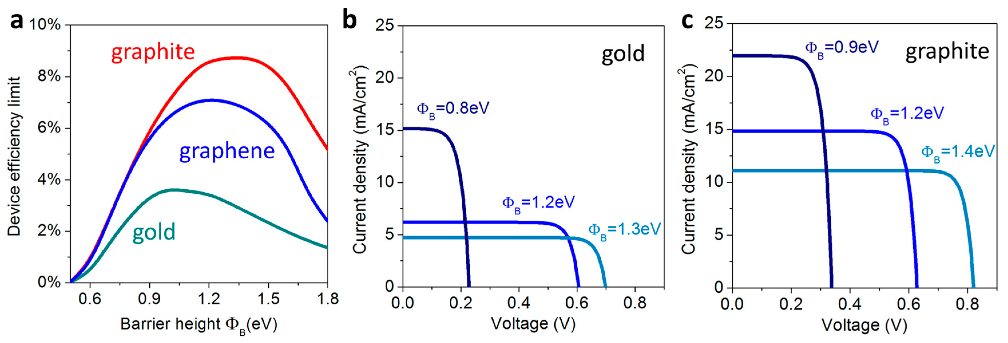
The upper limits of the overall conversion efficiency calculated using Equation (4)–(7) for Au, graphene and graphite are plotted in
Figure 5a as a function of the Schottky barrier height. All the plots have a characteristic bell shape, exhibiting efficiency reduction for low barrier heights due to the enhanced thermionic reverse current, and a similar drop at high barrier heights due to the reduced number of hot electrons with high enough energy to cross the potential barrier.
Typical I–V curves for several barrier heights are shown in
Figure 5b,c for gold and graphite devices, and illustrate the common trend of the short circuit current increase (decrease) at the expense of reduced (increased) open circuit voltage at low (high) barrier heights. The I–V curves for graphene look very similar and were omitted for brevity. The data in
Figure 5a predict that graphite can potentially offer an over twofold increase in the overall device efficiency over Au, reflecting the larger population of energetic electrons photo-generated in graphite (
Figure 2) and the corresponding higher IPE efficiency (
Figure 3). The optimum barrier height for the graphite-based device is higher than those for the Au- and graphene-based devices, but graphite is expected to outperform the other materials at any barrier height. The efficiency limit increase of the graphite-based IPE device over that of graphene-based device is not as significant as over the Au-based platform. However, this limit assumes 100% light absorption across the broad solar spectrum, and thus the actual efficiency is expected to be much higher for graphite than graphene IPE devices due to significant difficulties in achieving efficient broadband absorption in two-dimensional graphene monolayer.
4. Increasing Efficiency Levels with Solar Concentration and Spectral Splitting Strategies
Similar to the Shockley–Queisser limit of the photovoltaic cells, the conversion efficiency of the IPE converter with the graphite absorber can be further increased by using either solar concentration or spectral splitting (or both) [
1,
48]. Sorting solar photons by their energies and processing different parts of the solar spectrum separately by using several conversion platforms is a well-known way to increase the light-to-current energy conversion efficiency [
1,
49,
50]. Single-junction PV cells can only efficiently convert photons with energies within the so-called PV band just above its electron bandgap [
1,
51,
52]. Higher-energy photons are absorbed efficiently in the cell yet their energy is partially lost during the charge-carrier thermalization process [
53,
54]. In turn, photons with low energies are not harvested by the PV cell at all. To achieve high overall energy conversion efficiency, PV cells can be incorporated into hybrid spectral-splitting energy conversion platforms [
1,
49,
51,
52], where high- and low-energy photons are processed by different converters.
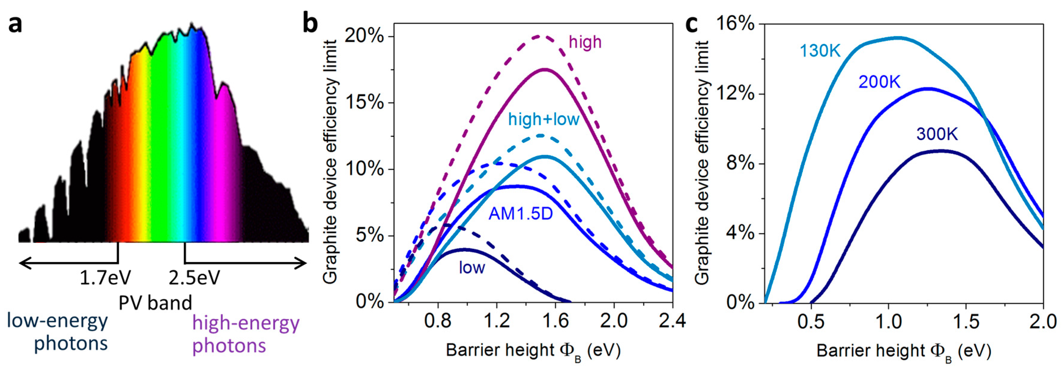
In
Figure 6 we evaluate the possibility of using the graphite IPE device as a part of the hybrid solar energy conversion platform, which also incorporates a conventional photovoltaic cell.
Figure 6a schematically shows one of many possible ways of splitting the solar spectrum into three parts: high-energy band, low-energy band, and the central PV band. The data in
Figure 6b show that the conversion of only high-energy and low-energy parts of the solar spectrum can be performed at an efficiency higher than that of the full-spectrum conversion (compare the solid blue and light blue lines in
Figure 6b). The PV band of the solar spectrum can then be directed to a conventional photovoltaic cell with the help of selective mirrors or filters [
1,
51] to be converted at high efficiency. It should be noted that in this case the PV cell efficiency will also exceed its Shockley–Queisser [
54] limit owing to the elimination of the low- and high-energy parts from the photon spectrum [
1,
55]. The high-energy part of the solar spectrum alone (solid purple line in
Figure 6b) can be converted by the graphite IPE converter at a much higher efficiency than the whole broadband solar spectrum (solid blue line in
Figure 6b). Even the low-energy part of the solar spectrum can be converted to electricity with ~4% efficiency by a graphite-based IPE device (solid navy line in
Figure 6b).
The conversion efficiency of the IPE converter with the graphite absorber can be further increased by concentrating sunlight with external optics to increase photon flux [
1,
48]. Our calculations predict that for illumination with the concentrated sunlight of 100 suns, the efficiency maximum for the full spectrum processing increases and exceeds 10% (dashed blue lines in
Figure 6b). The efficiency plot retains its bell shape, with the maximum point shifting towards lower barrier height. Solar concentration increases the device efficiency limit for any spectral band, as can be seen by comparing the dashed lines (100 suns concentration) to solid lines (one sun) of the same color for different spectra windows in
Figure 6b. These results indicate a promising way of using the IPE converters as a part of hybrid solar harvesting and conversion platforms, especially at higher optical concentrations.
The temperature of the device is another parameter that can be tuned to improve its overall energy conversion efficiency. Since reverse thermionic current scales as the second power with temperature (Equation (4)), low-temperature operation would increase the performance of the IPE device. This is illustrated in
Figure 6c, where the graphite IPE device efficiency for the full solar spectrum conversion is plotted as the function of the potential barrier height at different temperatures. It can be seen that the maximum efficiency of the graphite IPE device at 130 K is almost double of that at 300 K, making it a potentially promising platform for airborne and space applications.
5. Discussion and Conclusions
The above upper-limit efficiency analysis was performed under the assumption that all the solar energy can be absorbed by the (semi-)metal material in the IPE device, and that the photo-excited hot electrons can reach the barrier before they cool down [
39,
56]. In reality, a fraction of the photo-excited electrons will cool down before reaching the barrier. Hot carrier cooling occurs though a combination of electron–electron and electron–phonon scattering processes [
7,
57]. However, if the absorber thickness is comparable to or smaller than the hot carrier mean free path in the absorber material, multiple reflections of hot electrons from the surfaces of the thin film can take place, increasing the probability of the IPE process [
39]. It is known from prior measurements and DFT modeling that the mean free path for hot electrons in noble metals such as Au range from a few nanometers for electrons with energies exceeding the Fermi level by 2–5 eV, to 50–100 nm for electrons with energies close to the Fermi level [
9]. Recent DFT modeling predicts comparable mean free path values for higher-energy electrons in graphene and graphite, and significantly larger ones (from ~100 nm to above 1000nm) for electrons with energies within 0.5eV above the Fermi level [
58]. Furthermore, unlike in noble metals, electron–phonon scattering is predicted to be the dominant scattering process for the non-equilibrium electrons, especially for those with higher energies. This effect was attributed to softer phonon modes and stronger electron–phonon coupling with lighter atoms in carbon materials than in metals [
58]. The above observations hold high promise for the use of hot-carrier carbon IPE devices as photodetectors for both visible and infrared spectral ranges [
12,
59].
Graphene has already been actively explored for hot-electron harvesting applications [
60,
61,
62]. However, achieving efficient broadband absorption in graphene is significantly more challenging than in either gold or in graphite [
63]. The use of graphite offers carbon-based efficient and broadband light harvesting as well as electron characteristics more favorable for generating high-energy photo-excited charge carriers, which translates into higher IPE device efficiency. Schottky-junction IPE energy converters with graphite as the active absorber material can be fabricated with a variety of semiconductors, including Si, TiO
2, SiC, GaAs, etc., allowing for tuning and optimization of the potential barrier height [
24,
28]. Finally yet importantly, the price of graphite is orders-of-magnitude below that of gold owing to its much higher abundance in the earth’s core. While graphite costs about 1.5 K US dollars per metric ton, gold costs about 40 K US dollars per kilogram [
64].
Overall, our data highlight the strong effect that the material’s electron density of states structure can have on the efficiency of the solar-harvesting IPE devices. Our results also illustrate that the electron density of states in graphite together with the long hot electron mean free path, low price, and abundance makes it a promising IPE absorber material candidate for harvesting visible and near-infrared photons. The technique described in this paper offers a useful strategy to screen other potential material candidates for use as absorbers in IPE photo-detectors and photon energy harvesters. It can also be used to engineer new nanostructured materials (including carbon materials) with tailored electron density of states that maximizes device efficiency. An ideal absorber material that would maximize the high-energy hot electron population should exhibit a high and narrowband peak in its density of states just below the material Fermi level [
19]. The energy distribution of the graphite DOS is close to this ideal situation than that of Au, which contributes to the efficiency limit improvement predicted in this work. Further material improvements can be accomplished by using quantum confinement effects in heterostructures and alloys.


