A Novel Offset Cancellation Based on Parasitic-Insensitive Switched-Capacitor Sensing Circuit for the Out-of-Plane Single-Gimbaled Decoupled CMOS-MEMS Gyroscope

Abstract
: This paper presents a novel parasitic-insensitive switched-capacitor (PISC) sensing circuit design in order to obtain high sensitivity and ultra linearity and reduce the parasitic effect for the out-of-plane single-gimbaled decoupled CMOS-MEMS gyroscope (SGDG). According to the simulation results, the proposed PISC circuit has better sensitivity and high linearity in a wide dynamic range. Experimental results also show a better performance. In addition, the PISC circuit can use signal processing to cancel the offset and noise. Thus, this circuit is very suitable for gyroscope measurement.1. Introduction
Generally speaking, MEMS gyroscopes only have relatively small detection capacitances; therefore, the sensing circuit design is very important. The sensing mechanisms of MEMS gyroscopes are mainly categorized into piezoresistive [1–5] and capacitive [6–13] mechanisms. Capacitive gyroscopes have simpler structure and hence lower fabrication cost. In addition, they provide lower power consumption, higher sensitivity, and higher reliability as well as lower nonlinearity, lower temperature dependency, lower noise, and lower drift. Capacitance is also easily available in silicon technology because it does not require special materials and process steps. On the other hand, the piezoresistive sensing scheme is widely used in accelerometers. If the gyroscopes use piezoresistive materials, they should be driven in their primary modes with different mechanism because piezoresistive materials cannot induce passive nature by themselves [14]. In addition, its sensitivity is low, and its temperature dependency is high compared to the capacitive gyroscope. Hence, it is mainly used in low-end products.
Capacitive sensing circuits are categorized into synchronous [15], switched-capacitor [12,16–18], and fully differential circuits [8,11,19,20]. The transfer functions of the first two are independent of parasitic capacitance, and they can cancel the flicker noise and DC offset voltage to provide high accuracy. The synchronous sensing circuit requires bias control with either a large value off-chip or large-area integrated resistive circuit component [15]. In addition, in the frequency response, the transfer function of the synchronous sensing circuit has a zero point that increases the phase delay so that it cannot control feedback. The architecture of the fully differential sensing circuit is simple and contains no charge cancellation error, but its signals are attenuated by parasitic capacitance [19]. The switched-capacitor circuit technique is based on the realization that the capacitor and switch are equivalent to a resistor for reducing the layout area [16–18]. This technique can realize a variety of other signal-processing blocks, such as gain-stage, voltage-controlled oscillators (VCOs), and modulators. The switched-capacitor circuit can provide stability but it reduces the open-loop gain. In addition, the switched-capacitor circuit provides a virtual ground and robust DC biasing at the sensing node so that the sensed signal is insensitive to parasitic capacitance and undesirable charging. This circuit also offers a wide range of techniques to suppress offset and low-frequency noise, such as correlated double sampling (CDS) and programmable capacitor array (PCA). Thus, this circuit is very suitable for gyroscope measurement. A novel parasitic-insensitive switched-capacitor (PISC) sensing circuit is designed in order to get high sensitivity and ultra linearity and reduce the parasitic effect for the out-of-plane single-gimbaled decoupled gyroscope (SGDG) in this study.
This paper is organized as follows: in Section 2, the PISC circuit design is briefly introduced. The simulation results are presented in Section 3. The experimental results are presented in Section 4. Finally, the conclusions are given in Section 5.
2. Circuit Design
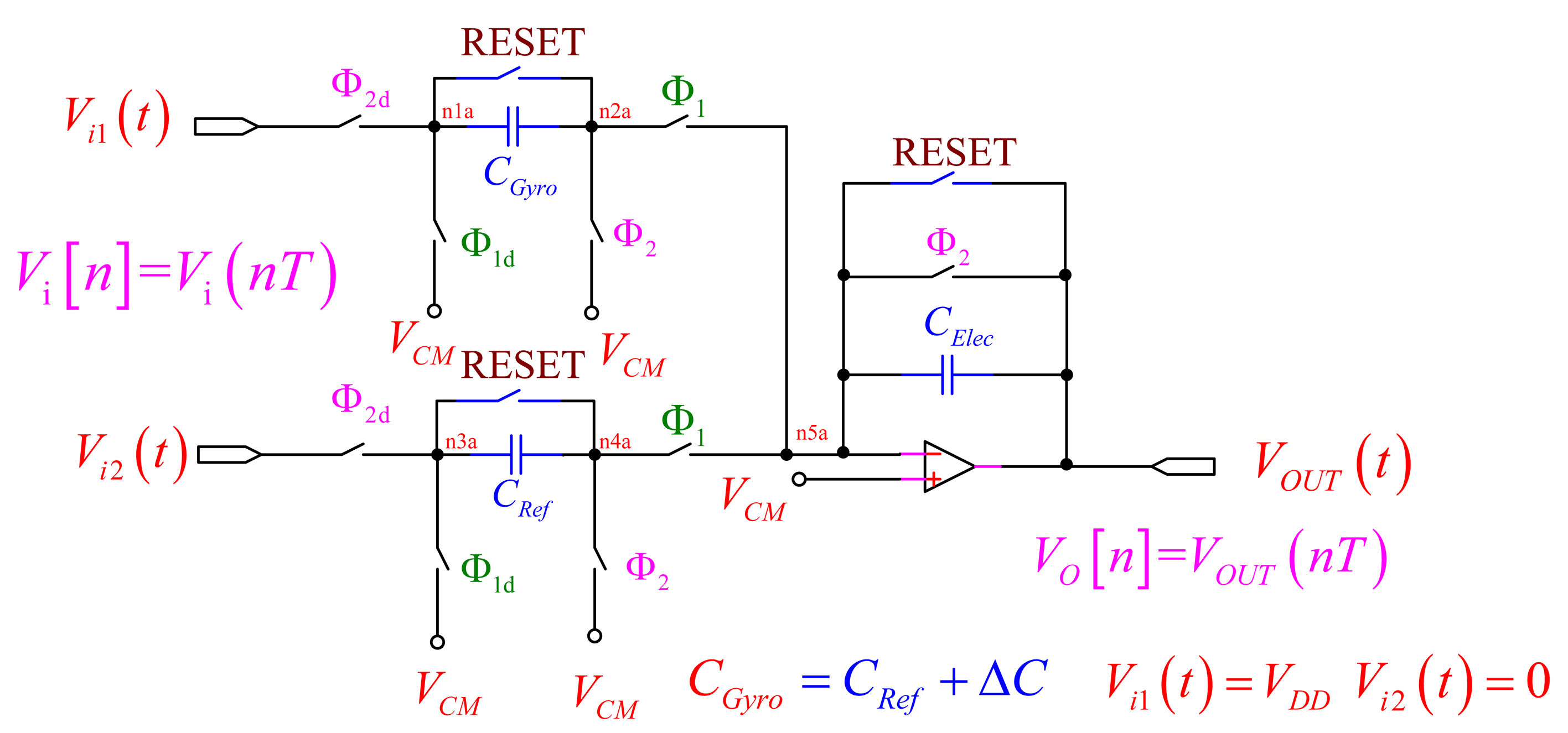
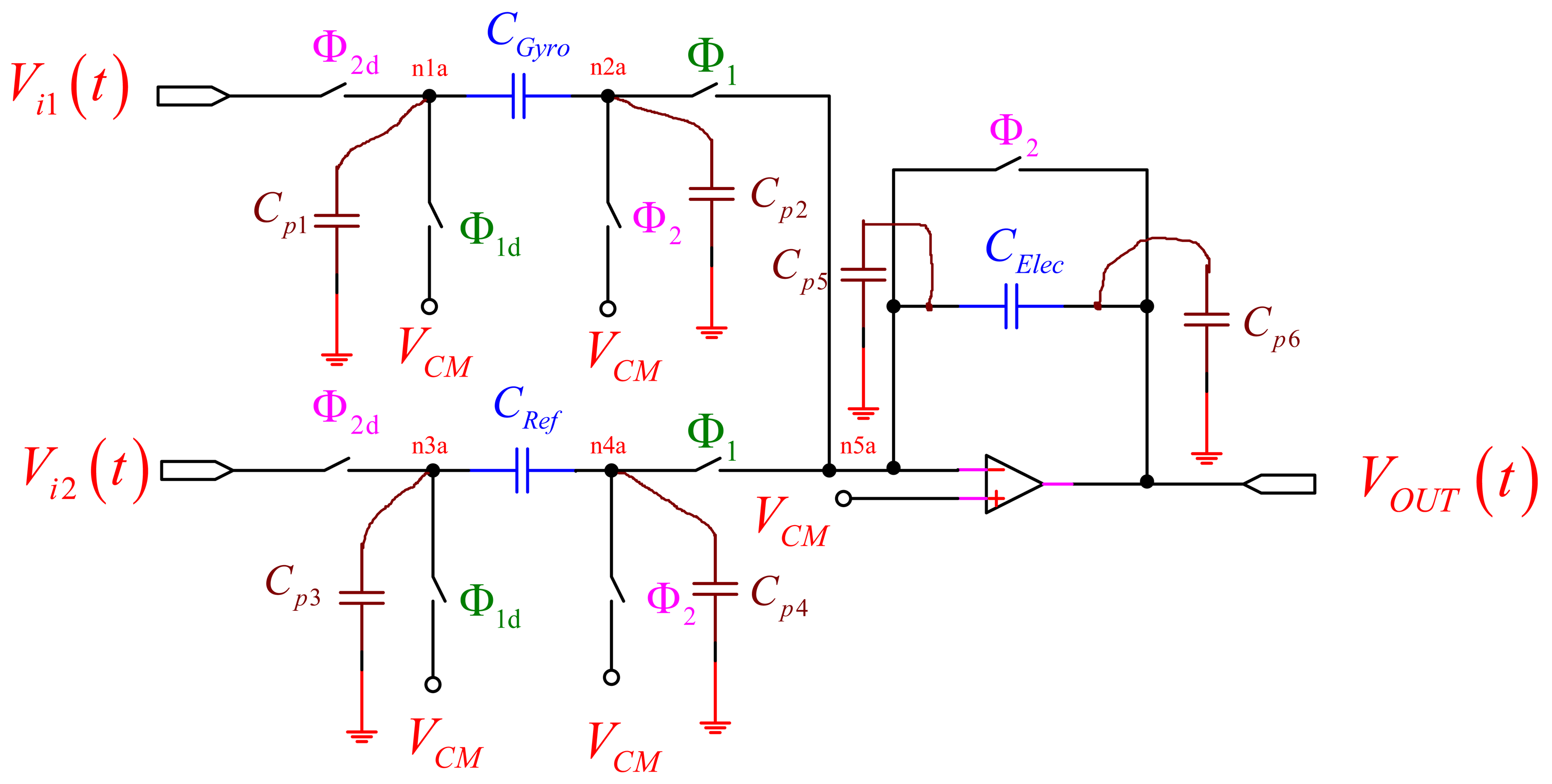
The on-chip sensing circuit uses the switched-capacitor sensing circuit that detects the capacitance change due to the deflection of the proof mass. During the sampling phase of a traditional switched-capacitor amplifier, it only samples the input, sets the output to zero, and provides no amplification. This raises concern about its stability, and reduces the open-loop gain. The capacitors used are known as double-poly capacitors. There also exists a substantial parasitic capacitance. In order to reduce the parasitic effect, we propose the PISC sensing circuit, as shown in Figure 1 [16,17]. Here, the “RESET” switches are only utilized for discharging the capacitors initially. The CGyro is capacitance of detection of the gyroscope, the CRef is initial capacitance of detection of the gyroscope and the CElec is amplification capacitance. VCM is common mode voltage, and its value is VDD/2. In this study, the VCM is set to 1.65 V.
At the beginning, the input signals voltages of the circuit are +1.65 V and −1.65 V. In order to maintain the cut-off condition for all the substrate-to-channel junctions, the substrate is usually connected to the most negative power supply in an NMOS circuit (the most positive in a PMOS circuit) [18]. Thus, we use the concept of voltage translation to change the input signal voltage. The input signal Vi1(t) changes to VDD, and the other Vi2(t) changes to zero.
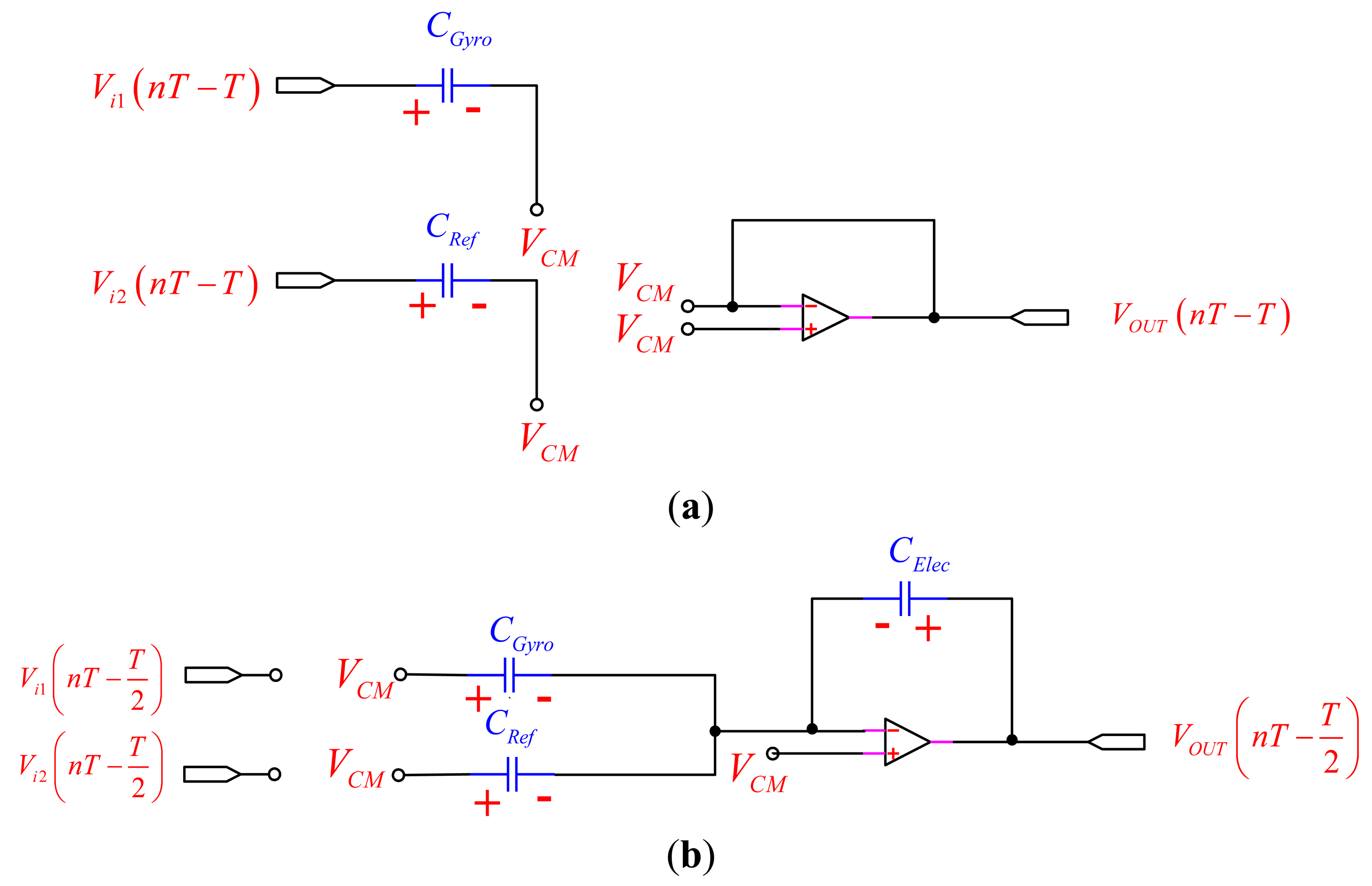
As shown in Figure 2(a), in the sampling mode, Φ2 is on and Φ1 is off, allowing the voltage across CGyro and CRef to track Vi1(t) and Vi2(t) while the operational amplifier (OP-amp) and CElec hold the previous value. In the transition to the amplification mode, the charge stored on CGyro and CRef are transferred to CElec through the virtual ground node, as shown in Figure 2(b).
The results in the transfer function for this switched-capacitor circuit are given by:
Note that Equation (1) represents its gain coefficient as the ratio of the difference capacitance and CElec. The z−1/2 represents a period delay and can be ignored [16]. The behavior of the circuit with respect to parasitic capacitances is plotted in Figure 3 [16].
Here, Cp1 is continuously being charged to Vi1(t) and discharged to the common mode (VCM). However, when Φ2 is turned on, the fact that Cp1 is also charged to Vi1(t − 1) does not affect the charge that is placed on CGyro. When Φ1 is turned on, Cp1 is discharged through the Φ1 switch attached to its node, and none of the discharging current passes through CGyro to affect the charge accumulating on CElec. Therefore, it does not affect the circuit operation. In addition, Cp2 is either connected to VCM through the Φ2 switch or to the virtual ground through the Φ1 switch. Since Cp2 always remains discharged, it does not affect the operation of the circuit. Similarly, the operations of Cp3 and Cp4 do not effect as Cp1 and Cp2. The effect of Cp5 on the transfer function is small since it is always connected to the virtual ground of the OP-amp. Finally, Cp6 is connected to the OP-amp output. Although it may affect the speed of the OP-amp, it would not affect the final settling point of the OP-amp output.
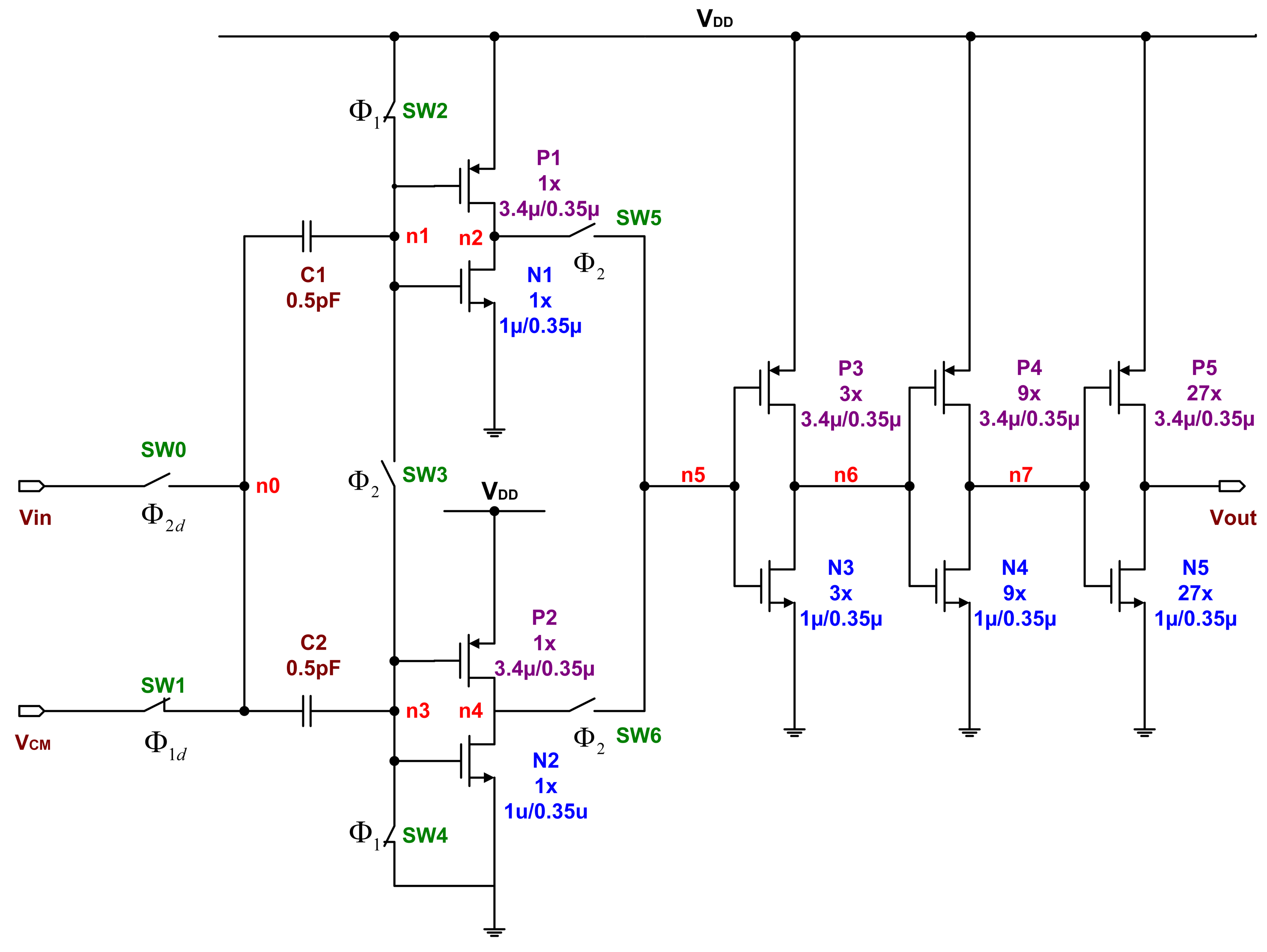
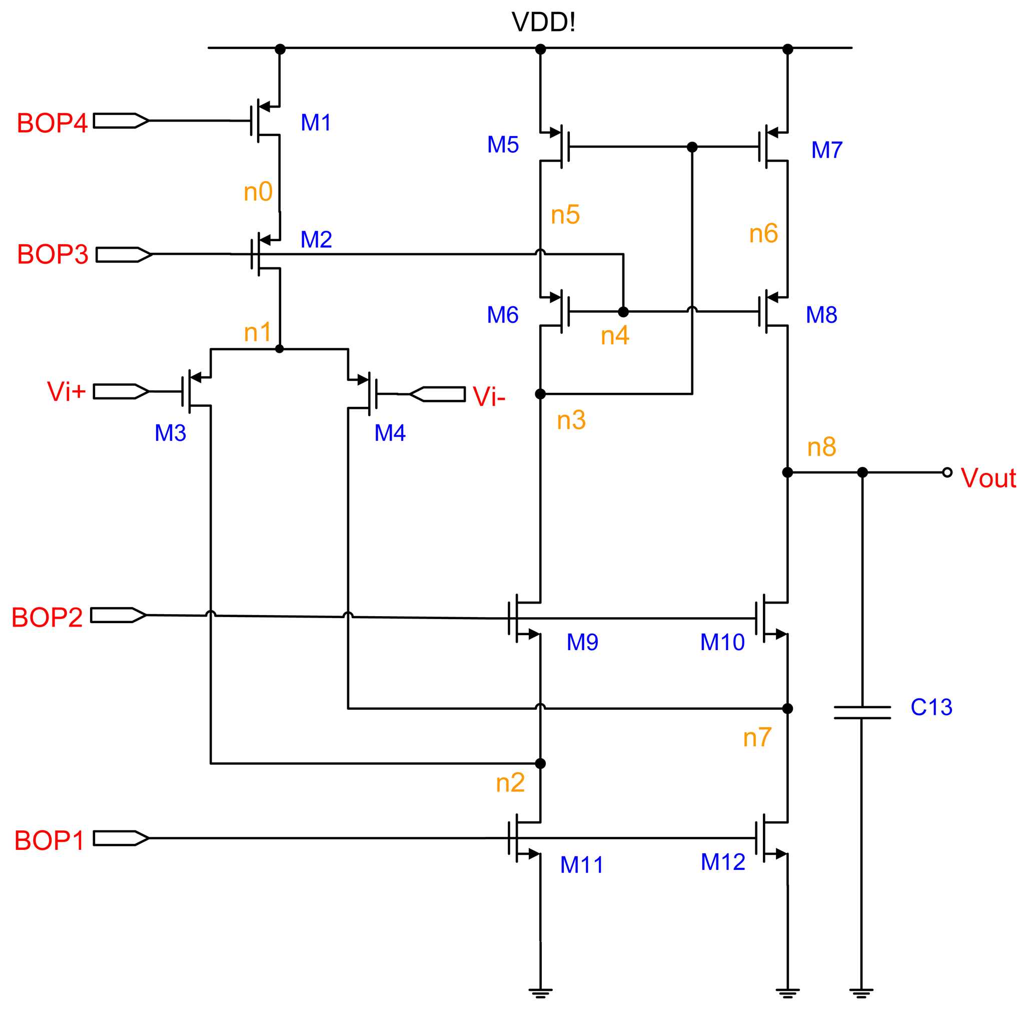
A switched-capacitor circuit is realized with basic building blocks such as the OP-amp, capacitors, switches, and non-overlapping clocks. The OP-amp circuit is shown in Figure 4. To improve the circuit stability, the OP-amp must provide a high enough stability margin. The folded-cascode OP-amp architecture is selected to provide the phase margin of 78.906°. The input differential pairs use large devices with a parallel symmetric layout for good matching, thereby reducing the input voltage offset and flicker (1/f) noise. To increase the phase margin of OP-amp, a large output compensation capacitor of up to 3.8 pF is used; it is made of double poly (poly1 and poly2). Table 1 provides a list of the device sizes.
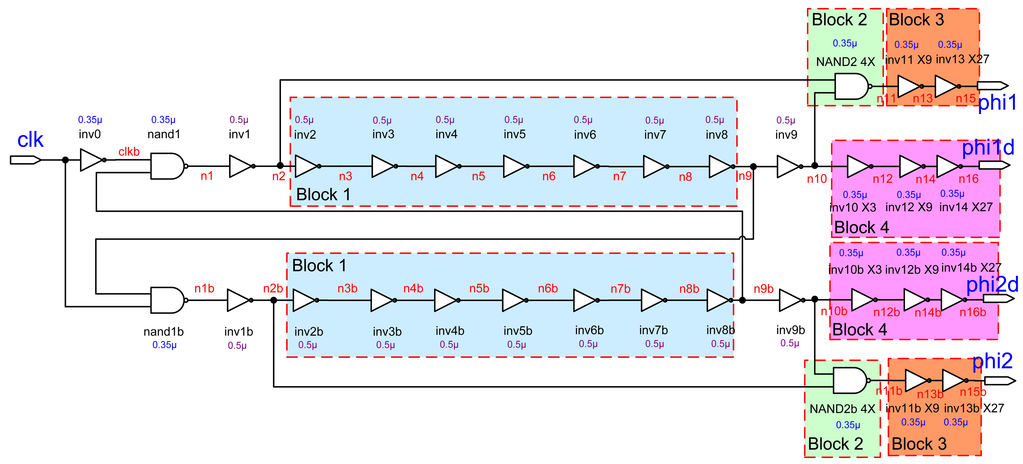
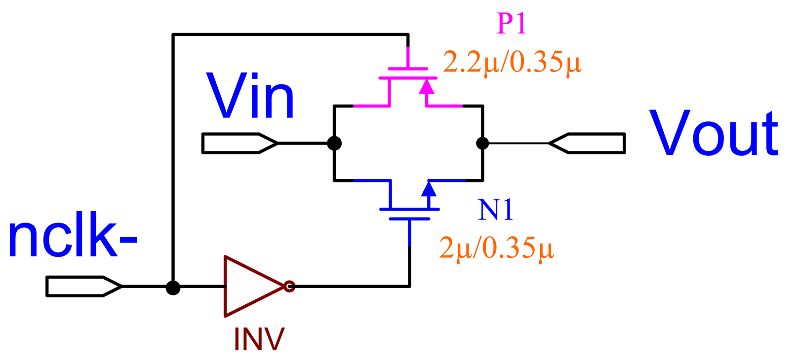
The requirements for switches used in this paper are that they have very high off resistance and low on resistance, and introduce no offset voltage when turned on. In order to achieve the full signal range of 0 to 3.3 V, we used a negative triggered CMOS transmission gate, as shown in Figure 5 [16]. To guarantee that the charge is not inadvertently lost, we adopt the non-overlapping clock, as shown in Figure 6, which is used to eliminate the clock feed-through influence [16,17]. It has two logic signals running at the same frequency and is changed in such a way that at no time are both signals high.
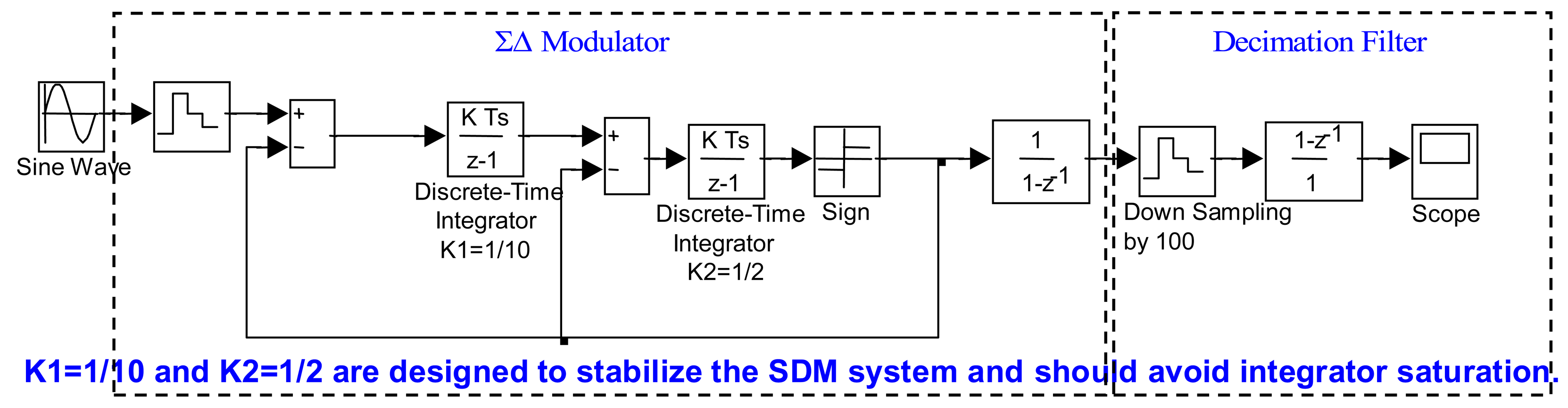
A sensing circuit usually requires an ADC. In general, the output voltage for the sensing circuit is weak and small. A high resolution ADC is necessary for acquiring such a feeble signal. The ΣΔ ADC is the best choice for this application. It uses the over-sampling principle, noise shaping and decimation filtering to achieve the high resolution. It consists of a ΣΔ modulator and a decimation filter. In addition, the ΣΔ ADC operates in the discrete-time domain and is implemented using the switch-capacitor circuit technique. The switch-capacitor circuit can only be realized in MOS devices, not in bipolar transistors. In other words, the sensing circuit fabricated in the digital CMOS process is suitable for generating the digital output using ΣΔ ADCs. The behavior simulation model shown in Figure 7 is adopted for the ΣΔ modulator design to avoid the integrator overload and to satisfy the system requirements. The design is the second order ΣΔ modulator with a one-bit quantizer. The decimation digital filter is implemented by down-sampling and a comb filter. The discrete-time integrator parameters of K1 and K2 for the ΣΔ modulator are 0.1 and 0.5, respectively.
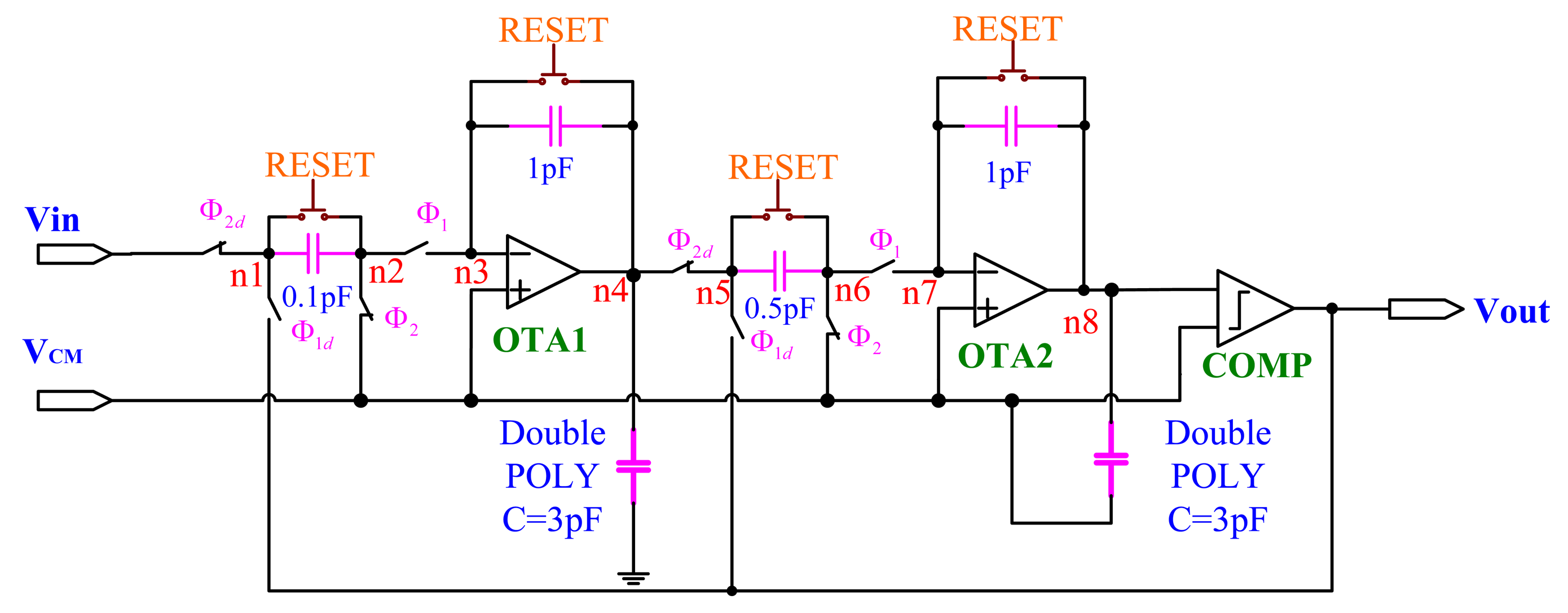
The circuit design for the ΣΔ modulator is shown in Figure 8. Here, “OTA1” and “OTA2” are folded-cascode OP-amps, as shown in Figure 4. The “COMP” indicates the comparator circuit, as shown in Figure 9. The “RESET” switches are only utilized for discharging the capacitors initially. The circuit is implemented using the switch-capacitor technique and controlled by a non-overlap clock circuit, as shown in Figure 6, which is used to eliminate the clock feed-through influence.
3. Simulation Results
In this paper, the simulation results for circuit design are the post-layout simulation results.
3.1. CRef Selection
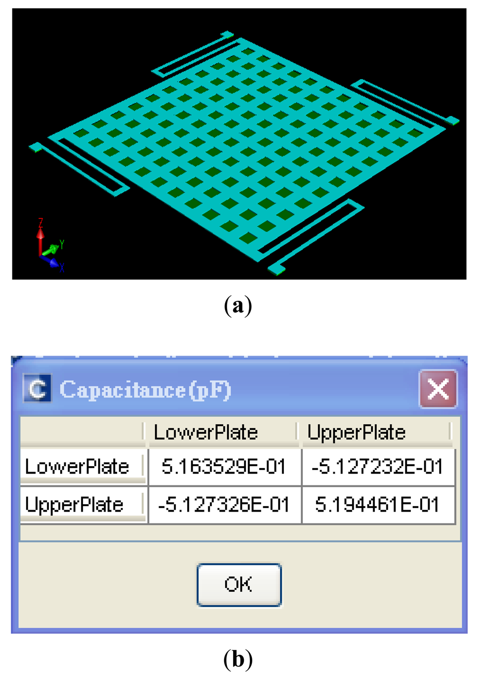
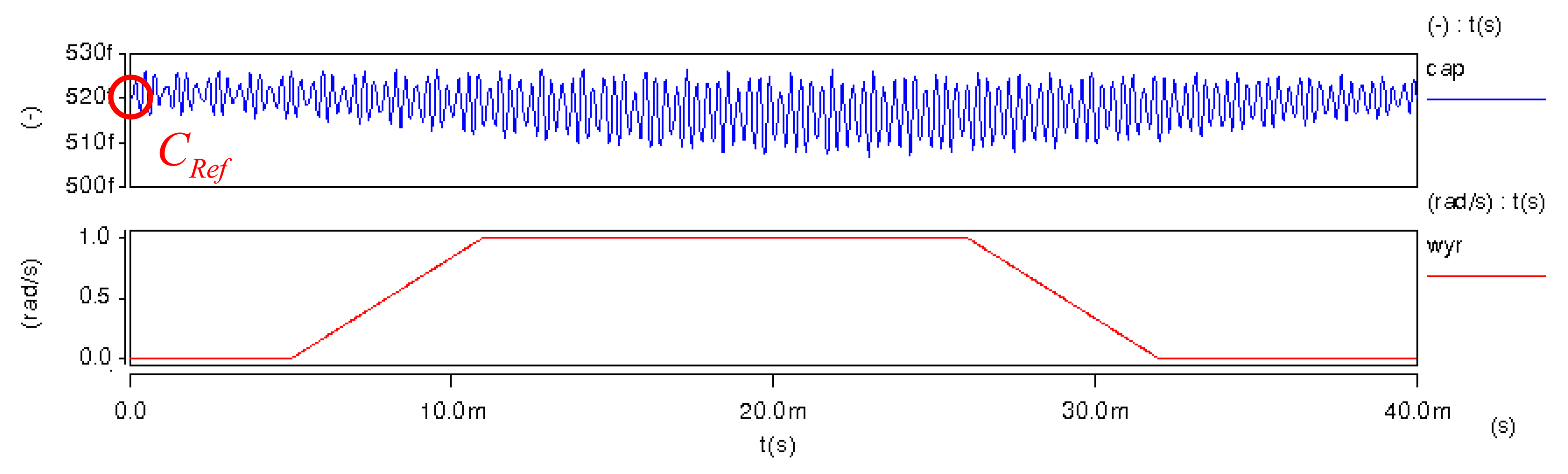
The CRef is the initial capacitance of detection for the gyroscope. The capacitance value is simulated using the CoventorWare FEM simulator. The simulator uses the solid model of the gyroscope (see Figure 10(a)) and its capacitance value is about 516 fF, as shown in Figure 10(b). In addition, we also use the ARCHITECT™ simulator to estimate CRef. It models the mechanical and electrical effects of these rough environments on the out-of-plane SGDG. In ARCHITECT™, we work in a schematic-driven environment using symbols to represent individual components or elements of components, as seen in Figure 11. Typically, these component models are parameterized. The simulation result of electrode capacitance (cap) for the transient analysis is shown in Figure 12. It can be found that the initial capacitance, CRef is about 519 fF when the sensing signal (wyr) is 1 rad/s. The capacitance is calculated to be about 499 fF by the formula. After comparing the three methods, we choose this value of about 500 fF for a convenient layout.
3.2. CElec Selection
In Table 2, the output voltage of CGyro = 500 fF is close to VCM (= 1.65 V) when CElec is 60 fF. Here, these output voltages are simulated by the HSPICE simulator. However, these values should be actually approached when CElec is 63 fF. But this time the layout is poor to achieve. Therefore, we choose CElec to be 60 fF.
3.3. Parasitic-Insensitive Switched-Capacitor Circuit
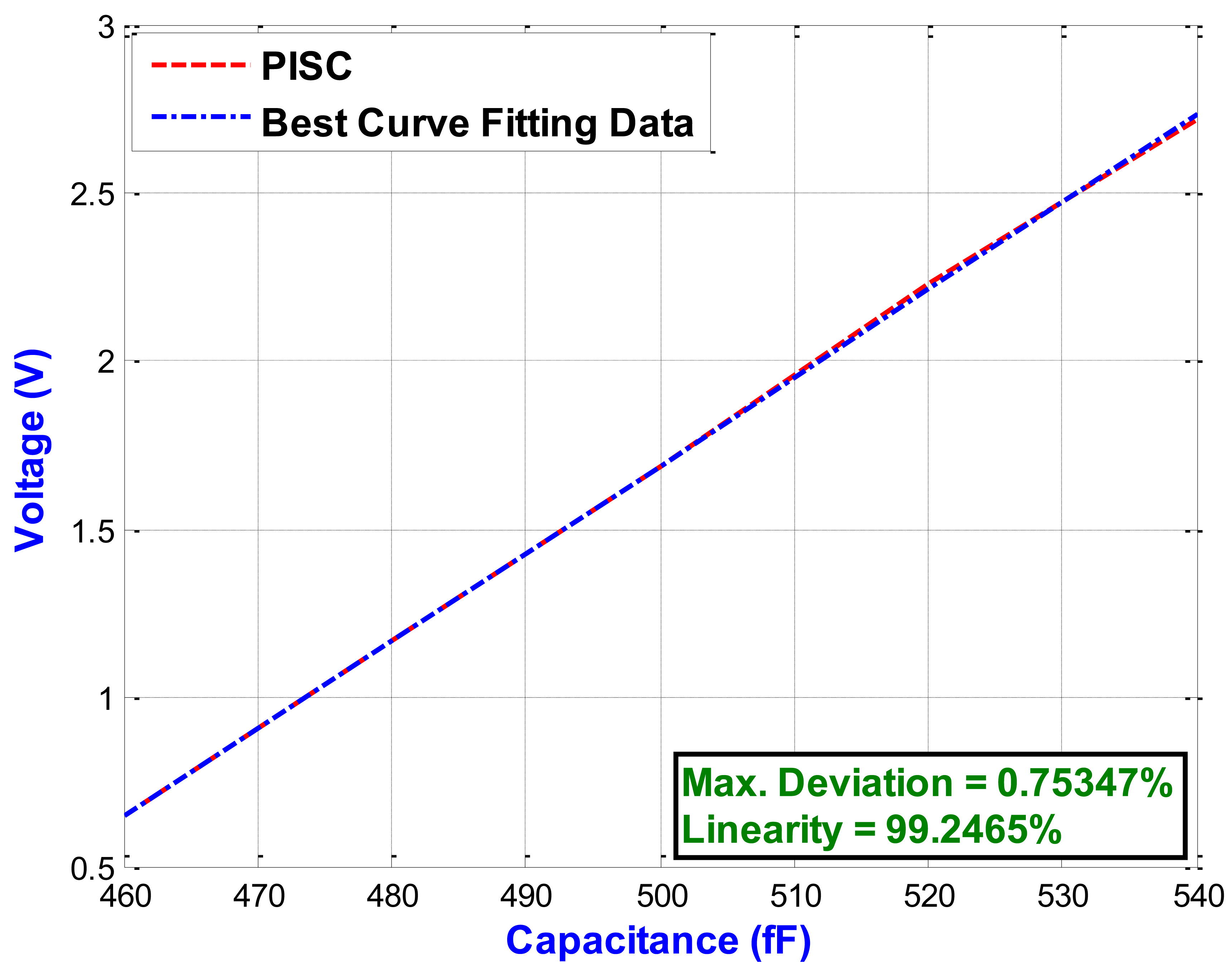
Figure 13 shows the C-V curves of the two capacitive sensing circuits, including the PISC circuit and simple non-inverting amplifier. The proposed PISC circuit has the higher dynamic voltage output and sensing range than those of the simple non-inverting circuit. Figure 14 illustrates the enlarging parts of the PISC circuit of Figure 13 between 460 fF and 540 fF.
The proposed PISC circuit has an ultra linearity of 99.2465%. The detailed specifications and comparisons of the two circuits are summarized in Table 3. It can be noted that the proposed PISC circuit has the higher capacitance sensitivity, lower power dissipation, and smaller noise floor, but its resolution and voltage offset are less than those of the simple non-inverting circuit. The main reason is that it uses more components than the simple non-inverting circuit.
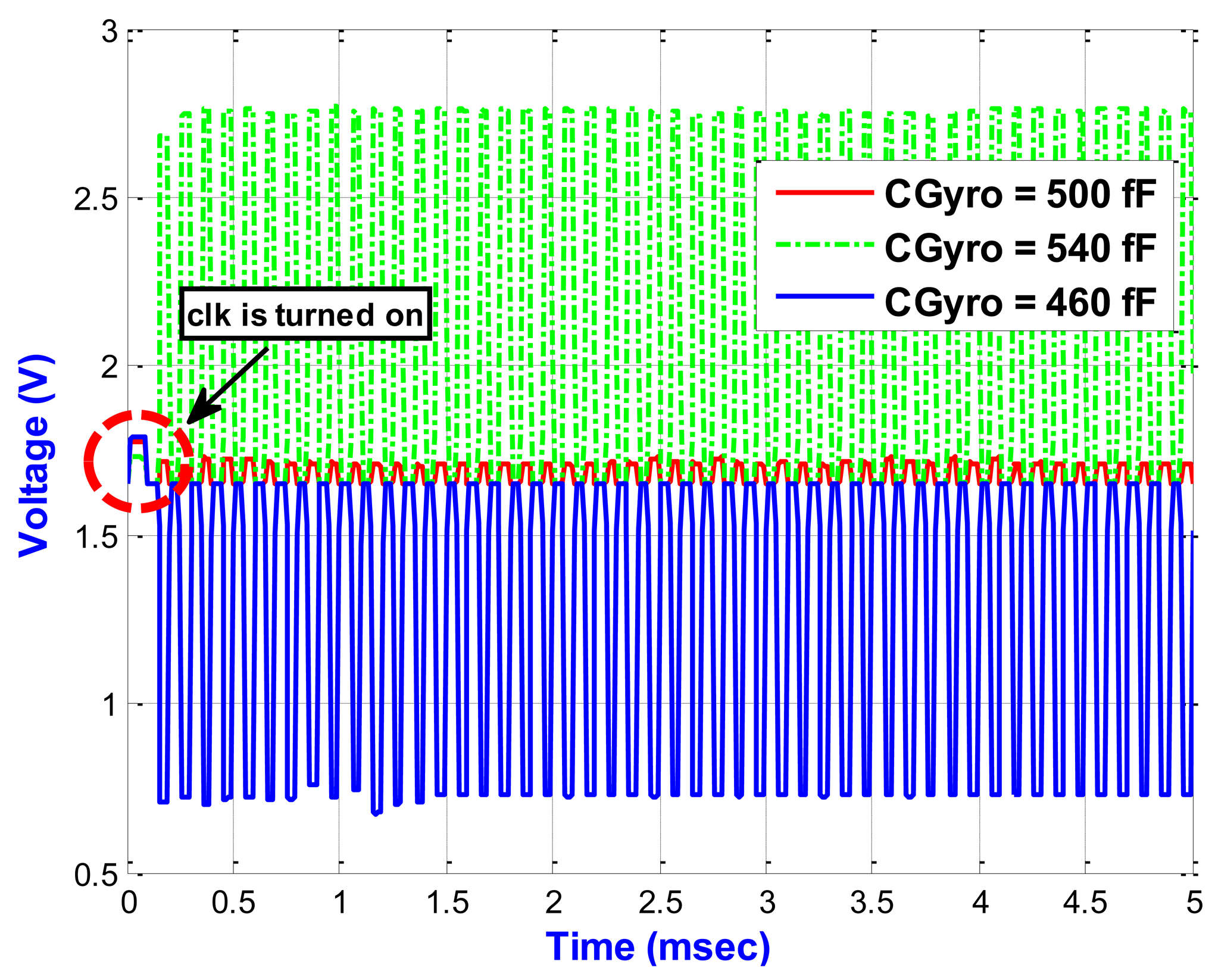
Figure 15 shows the output results of the proposed PISC circuit under different CGyro. When the time reaches 100 μs, the clk in Figure 6 is turned on. From the simulation results, we can see that the proposed PISC circuit starts sampling after clk is turned on. In addition, the PISC circuit with CGyro = 500 fF is mainly for the noise and offset signals. Thus, we can use signal processing to cancel the noise and offset, as shown in Figure 16.
Table 4 shows that the PISC circuit using signal processing has significantly smaller voltage offset and noise floor than those without using signal processing. Their improvement factors are 24.6% and 29.3%, respectively, compared to without using signal processing.
3.4. SDM (Sigma-Delta Modulator)
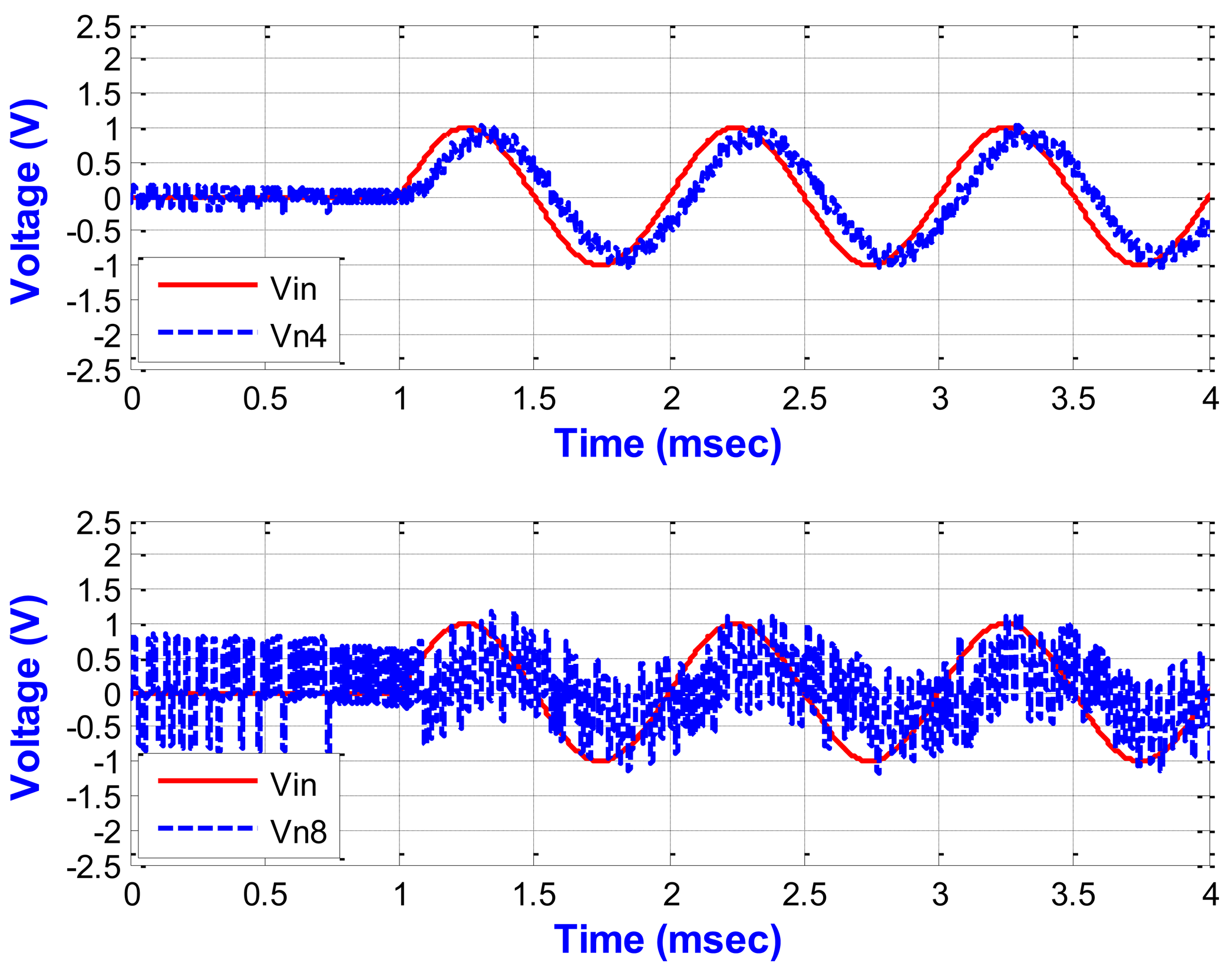
The simulation results of the SDM circuit simulated by HSPICE simulator from nodes of n4 and n8 in Figure 8 are shown in Figure 17 with a sinusoidal input.
Compared with the behavior simulation shown in Figure 7, they are almost the same. The bit-stream output of the ΣΔ modulator from the one-bit quantizer will be sent to the decimation filter to obtain the digital output.
3.5. Application (Combined Out-of-Plane SGDG in [21])
A single-gimbaled configuration is used to decouple the drive and sense modes of the gyroscope. Figure 18 shows the topology of the SGDG, which is a y-axis sensitive out-of-plane gyroscope. The gyroscope is driven in the drive-mode with three rows of symmetrical comb fingers. The main purpose is to increase the number of fingers to 206 pairs (see Figure 18), and to provide greater driving force, the amplitude of the driving displacement, and less thermo-mechanical noise. As depicted in Figure 18, four translational springs outside the frame constrain the degree-of-freedom (DOF), and hence the frame can be driven only along the x-axis. Inside the frame, another set of linear springs allows the proof mass to move solely along the z-axis. When an external angular rate is applied to the proof mass along the y-axis, the proof mass vibrates due to Coriolis force along the z-axis. The Coriolis force is sensed by four inner springs.
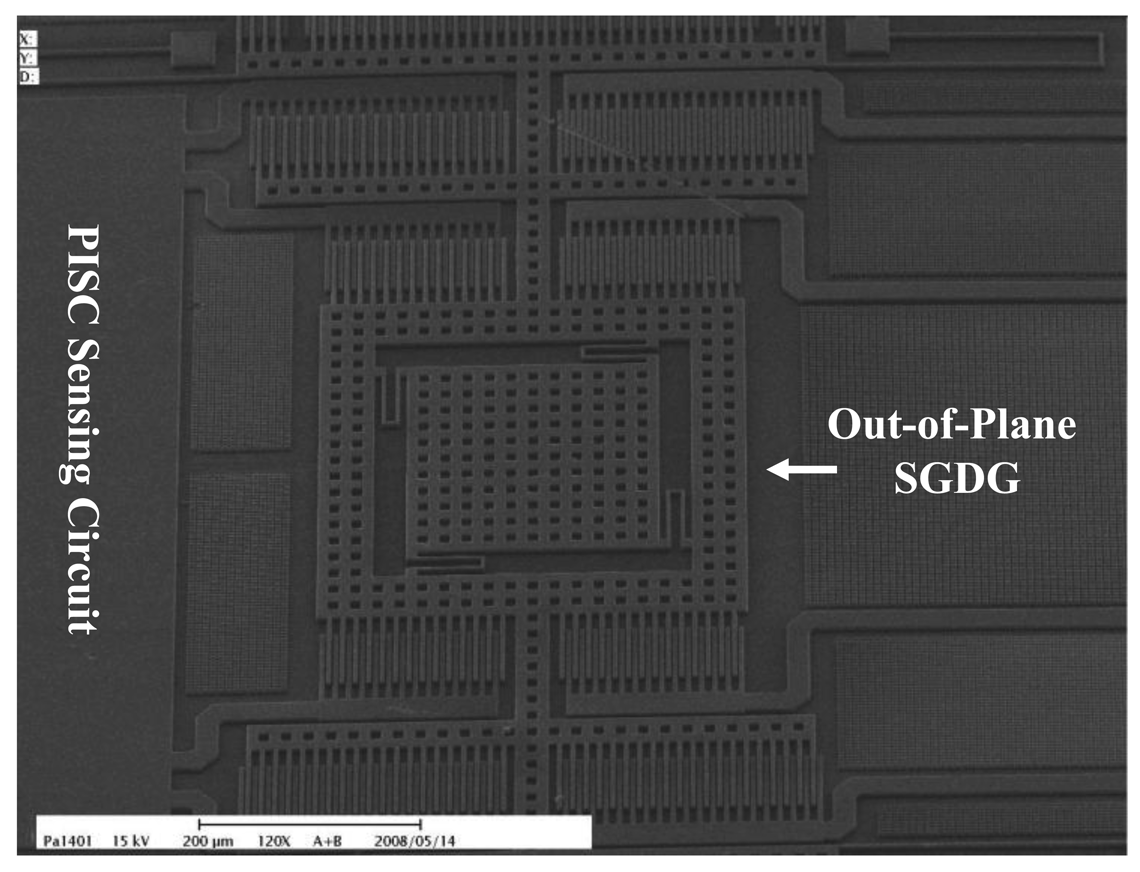
The frame and the proof mass are actuated by the electrostatic comb drives at the resonant frequency. The sense electrode under the proof mass detects the capacitance difference using the parallel plates. The gyroscope is designed as a symmetrical and decoupled gyroscope in order to achieve a high sensitivity. The springs are all identical in shape in two modes, the drive and sense modes, and have different mass values. However, due to spring constant difference in the drive and sense modes, and in order to cancel process variations in the resonant frequencies, the drive-mode has two symmetrical frequency tuning fingers. These fingers create the force in the drive-mode and may reduce the frequency in some ranges relative to the applied DC voltage. The top view of the gyroscope chip, shown in Figure 19, is 1.725 mm × 1.515 mm and contains the SGDG and PISC blocks. The PISC circuit is located on the left of Figure 19. To avoid the damage caused by etching silicon dioxide in the wet etch, the PISC circuit is placed 50 μm away from the out-of-plane SGDG. Except for the microstructure, the whole chip area is covered by the top metal layer, M4.
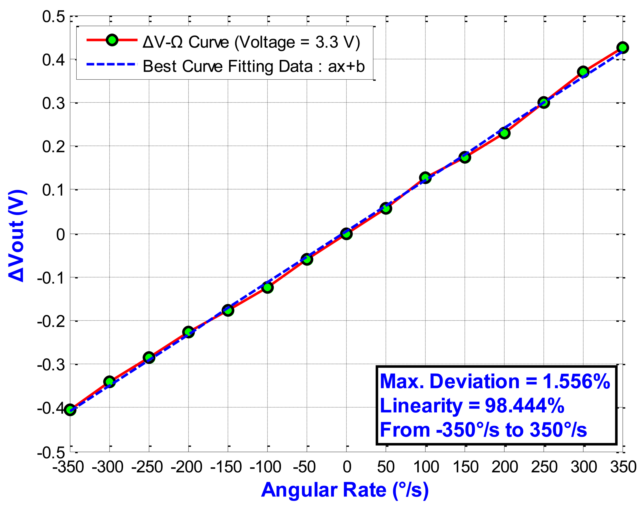
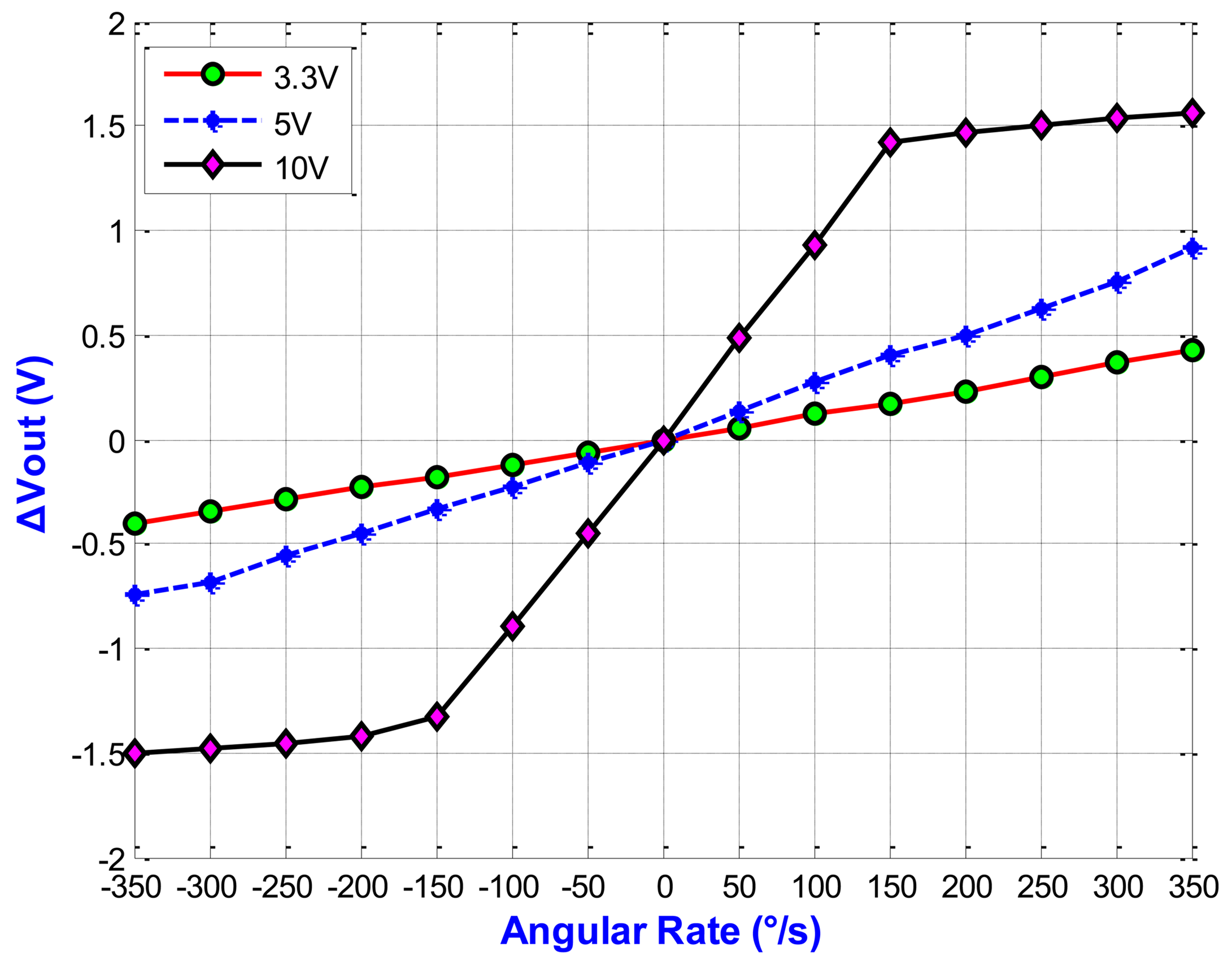
Figure 20 shows the output voltage of the gyroscope according to angular rate (VDriving = 3.3 V). Here, the VDriving means the driving voltage of the driving mode fingers. The sensitivity is 1.1866 mV/°/s and the linearity is 98.44% (with a full scale of 700 °/s). Figure 21 shows the output voltage versus the angular rate under different VDriving. For VDriving = 10 V, the sensitivity is 9.16 mV/°/s and the linearity is 99.16% (with a full scale of 300 °/s). The results of the out-of-plane gyroscope are summarized in Table 5.
4. Experimental Results
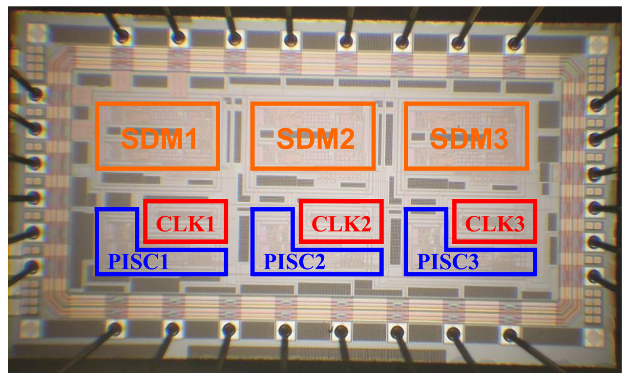
The proposed PISC circuit combined one-bit SDM circuit has been tested. The chip, shown in Figure 22, is 2.817 mm × 1.513 mm, and contains three PISCs, three CLKs, and three SDM blocks.
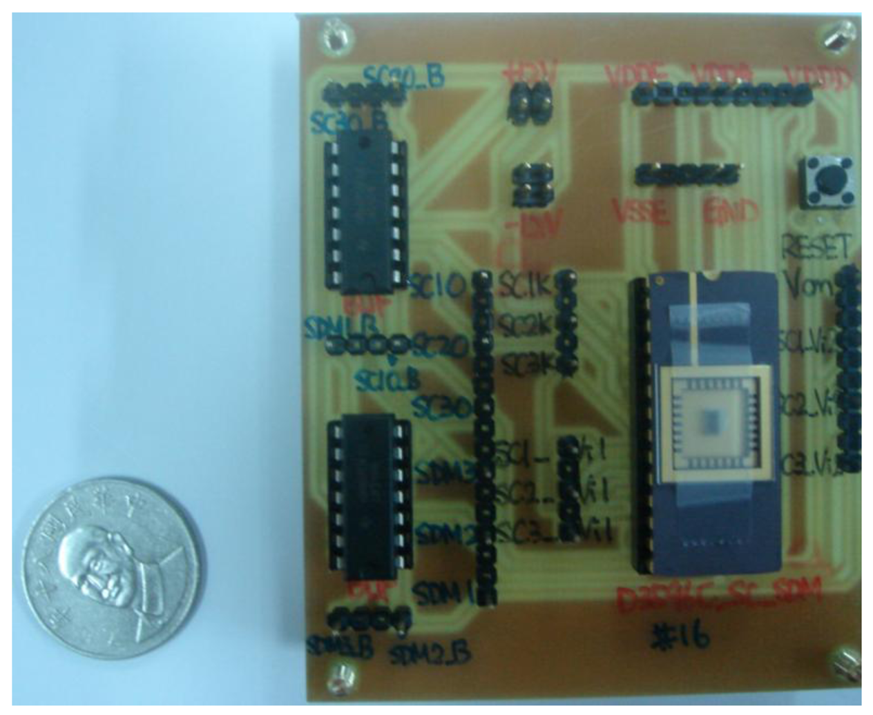
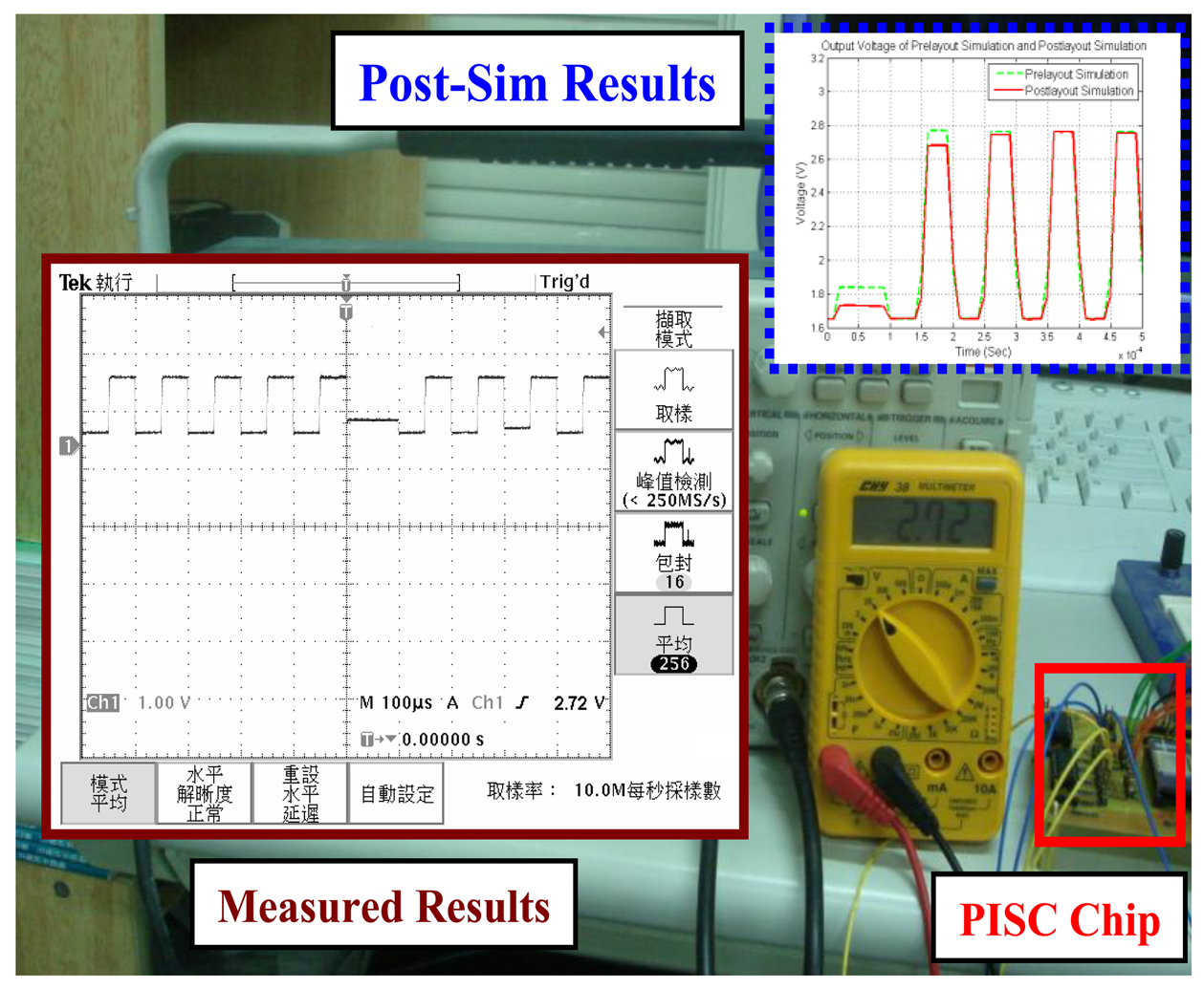
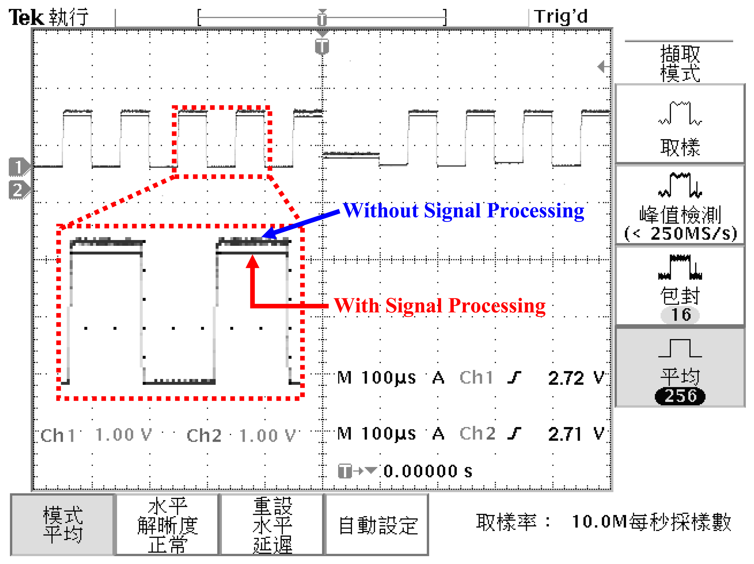
Here, the PISC1 means the PISC circuit has the CGyro = 500 fF, the PISC2 means the PISC circuit has the CGyro = 540 fF, and the PISC3 means the PISC circuit has the CGyro = 460 fF. CLK indicates the non-overlapping clock circuit. A photograph of the test PCB block is shown in Figure 23. The measured voltage result for the PISC2 circuit (CGyro = 540 fF) is 2.72 V, as shown in Figure 24. The pre- and post-layout simulation results are shown in the up-right corner in Figure 24. These results are very similar. Other results are summarized in Table 6. The experimental results of the PISC circuit using signal processing have significantly smaller voltage offset and noise floor than those without using signal processing, as shown in Figure 25.
Table 7 summarizes a comparison on the results of the proposed PISC circuit and other capacitive sensing circuits reported in the literature. It can be noted that the proposed PISC circuit has the smallest noise floor and chip area. The voltage offset is comparable to [11] but smaller than the remaining solutions listed in Table 7. The capacitive sensing circuits in [11] is simulation result. The resolution is comparable to [12] but smaller than other capacitive sensing circuits already presented in the literature. For standalone applications, the device gives an analog output and provides digital output with embedded one-bit ΣΔ ADC.
5. Conclusions
In this study, we present a novel PISC sensing circuit design in order to obtain high sensitivity and ultra linearity for an out-of-plane gyroscope. From the simulation results, we can see that the proposed PISC circuit has a good sensitivity of 9.16 mV/°/s and a high linearity of 99.16% in a wide dynamic range from −300 °/s to 300 °/s. The experimental results also show a good performance. In addition, the PISC circuit can use signal processing to cancel the offset and noise. Thus, this circuit is very suitable for gyroscope measurement.
Acknowledgments
The authors would like to thank the National Chip Implementation Center (CIC), Taiwan for chip fabrication. We are grateful to the National Center for High-performance Computing, Taiwan for computer time and facilities. This work is partially supported by National Science Council, Taiwan under Grant number NSC 100-2221-E-002-077-MY3.
References
- Chiou, J.C.; Lin, Y.J.; Shieh, L.J. Out-of-Plane CMOS-MEMS resonator with electrostatic driving and piezoresistive sensing. Proceedings of the 6th IEEE Conference on Nanotechnology, Cincinnati, OH, USA, 17–20 June 2006; pp. 929–932.
- Liu, J.; Du, K.; Wang, R.; Shi, Y. Research of meso-piezoresistive effect micromachined gyroscope. Proceedings of IEEE International Conference on Nano/Micro Engineered and Molecular Systems, Kaohsiung, Taiwan, 20–23 February 2011; pp. 1–4.
- Nakano, S.; Toriyama, T.; Sugiyama, S. Sensitivity analysis for a piezoresistive rotary movement micro gyroscope. Proceedings of the International Symposium on Micromechatronics and Human Science, Nagoya, Japan, 9–12 September 2001; pp. 87–92.
- Shi, Y.; Wang, R.; Du, K.; Liu, J. Research on micromachined gyroscope with electrostatic drive and meso-piezoresistive detection. Adv. Mater. Res. 2010, 154-155, 119–123. [Google Scholar]
- Song, Z.; Chen, X.; Huang, S.; Wang, Y.; Jiao, J.; Li, X. A high-sensitivity piezoresistive gyroscope with torsional actuation and axially-stressed detection. IEEE Sensors, Toronto, Canada, 22–24 October 2003; 1, pp. 457–460.
- Erismis, M.A. MEMS accelerometers and gyroscopes for inertial measurement units. M.S. Thesis, Graduate School of Natural and Applied Sciences, Middle East Technical University, Ankara, Turkey, 2004. [Google Scholar]
- Fang, R.; Lu, W.; Wang, G.; Tao, T.; Zhang, Y.; Chen, Z.; Yu, D. Capacitor mismatch auto-compensation for MEMS gyroscope differential capacitive sensing circuit. Proceedings of IEEE International Conference on Electron Devices and Solid-State Circuits, Tianjin, China, 17–18 November 2011; pp. 1–2.
- Lobur, M.; Holovatyy, A. Overview and analysis of readout circuits for capacitive sensing in MEMS gyroscopes (MEMS angular velocity sensors). Proceedings of the 5th International Conference on Perspective Technologies and Methods in MEMS Design, Polyana-Svalyava, Zakarpattya, Ukraine, 22–24 April 2009; pp. 161–163.
- Miskam, M.A.; Sidek, O.; Ruhaifi, A.Z. Analysis of capacitive microelectromechanical system accelerometer proposed with voltage reference in read-out circuit. J. Appl. Sci. 2009, 9, 1658–1667. [Google Scholar]
- Rödjegård, H.; Lööf, A. A differential charge-transfer readout circuit for multiple output capacitive sensors. Sens. Actuat. A Phys. 2005, 119, 309–315. [Google Scholar]
- Sadat, A.; Yuan, J.S.; Xie, H. Integrated wireless MEMS accelerometer for physiological activity monitoring. Proceedings of World Multi-Conference on Systemics, Cybernetics and Informatics, Orlando, FL, USA, 18–21 July 2004; pp. 1–6.
- Yin, L.; Liu, X.W.; Chen, W.P.; Zhou, Z.P. High resolution interface circuit for closed-loop accelerometer. J. Semicond. 2011, 32, 1–8. [Google Scholar]
- Zhou, K.; Sun, L.; Ge, F.; Yang, Z.; Yan, G. A capacitive readout circuit with DC sensing method for micromachined gyroscopes. Proceedings of the 7th IEEE International Conference on Nano/Micro Engineered and Molecular Systems, Kyoto, Japan, 5–8 March 2012; pp. 712–715.
- Senturia, S.D. Microsystem Design, 2nd ed.; Kluwer Academic Publishers: Boston, MA, USA, 2001. [Google Scholar]
- Boser, B.E. Electronics for micromachined inertial sensor. Proceedings of International Conference on Solid-State Sensor and Actuators, Chicago, IL, USA, 16–19 June 1997; pp. 1169–1172.
- Johns, D.A.; Martin, K. Analog Integrated Circuit Design; John Wiley & Sons: New York, NY, USA, 1997; pp. 394–406. [Google Scholar]
- Razavi, B. Design of Analog CMOS Integrated Circuits; McGraw-Hill Companies: New York, NY, USA, 2001; pp. 662–663. [Google Scholar]
- Sedra, A.S.; Smith, K.C. Microelectronic Circuits, 4th ed.; Oxford University Press: New York, NY, USA, 1998; pp. 941–944. [Google Scholar]
- Evans, I.; York, T. Microelectronic capacitance transducer for particle detection. IEEE Sens. J. 2004, 4, 364–372. [Google Scholar]
- Wongkomet, N. Position sensing for electrostatic micropositioners. Ph.D. Thesis, Department of Electrical Engineering and Computer Science, University of California, Berkeley, CA, USA, 1998. [Google Scholar]
- Chang, M.H.; Huang, H.P. Simulation and characterization of a CMOS-MEMS gyroscope with parasitic-insensitive sensing. Proceedings of IEEE International Conference on Advanced Robotics and its Social Impacts, Taipei, Taiwan, 23–25 August 2008; pp. 1067–1070.


| OP-amp | Sizes | |
|---|---|---|
| Components | Type | transistor: width/length/# of fingers capacitor: width/length/# of parallel/value |
| M1 | PMOS | 40 μm/1 μm/2 |
| M2 | PMOS | 40 μm/1 μm/2 |
| M3 | PMOS | 40 μm/2 μm/4 |
| M4 | PMOS | 40 μm/2 μm/4 |
| M5 | PMOS | 40 μm/2 μm/2 |
| M6 | PMOS | 40 μm/2 μm/2 |
| M7 | PMOS | 40 μm/2 μm/2 |
| M8 | PMOS | 40 μm/2 μm/2 |
| M9 | NMOS | 20 μm/1 μm/1 |
| M10 | NMOS | 20 μm/1 μm/1 |
| M11 | NMOS | 20 μm/2 μm/2 |
| M12 | NMOS | 20 μm/2 μm/2 |
| C13 | PIP | 2.1 μm/31.93 μm/9/3.8 pF |
| CGyro(fF) | CElec(fF) | |||||||||
|---|---|---|---|---|---|---|---|---|---|---|
| 10 | 20 | 30 | 40 | 50 | 60 | 70 | 80 | 90 | 100 | |
| 460 | 0.18 | 0.203 | 0.235 | 0.308 | 0.488 | 0.661 | 0.79 | 0.889 | 0.994 | 1.032 |
| 500 | 1.88 | 1.808 | 1.748 | 1.730 | 1.722 | 1.691 | 1.71 | 1.692 | 1.693 | 1.685 |
| 540 | 3.12 | 3.104 | 3.050 | 2.982 | 2.830 | 2.688 | 2.55 | 2.454 | 2.380 | 2.305 |
| Term | PISC | Simple Non-inverting Amplifier |
|---|---|---|
| Supply Voltage (V) | 3.3 | 3.3 |
| Power Dissipation (mW) | 2.4108 | 2.4392 |
| Dynamic Voltage Output (V) | 0.0445–3.2427 | 1.6752–3.2434 |
| ΔC Range (fF) | ±40 | 0–40 |
| Sensing Range (fF) | 440–540 | 0–40 |
| Capacitance Sensitivity (mV/fF) | 25.8938 | 24.9875 |
| Linearity (%) | 99.2465 | 98.5426 |
| Ideal Resolution (fF) | 0.01273 | 0.00962 |
| Voltage Offset (mV) | 1.9964 | 1.5534 |
| Noise Floor (μV/Hz1/2) (at 10 kHz) | 0.1564 | 4.6716 |
| Term | Without Signal Processing | With Signal Processing | Improvement Factor (%) |
|---|---|---|---|
| Voltage Offset (mV) | 1.9964 | 1.5053 | 24.6 |
| Noise Floor (μV/Hz1/2) (at 10 kHz) | 0.1564 | 0.1106 | 29.3 |
| Parameters | 3.3 V | 5 V | 10 V |
|---|---|---|---|
| Sensitivity (mV/°/s) | 1.1866 | 2.3882 | 9.16 |
| Dynamic Range (°/s) (Full Scale) | 700 | 600 | 300 |
| Linearity (%) | 98.44 | 98.28 | 99.16 |
| Term | Simulation Results | Experimental Results |
|---|---|---|
| Supply Voltage (V) | 3.3 | 3.3 |
| PISC1 (V) | 1.65–1.78 | 1.6–1.81 |
| PISC2 (V) | 1.65–2.78 | 1.6–2.8 |
| PISC3 (V) | 0.7–1.65 | 0.7–1.6 |
| [7] | [10] | [11] | [12] | [13] | [19] | This Work | |
|---|---|---|---|---|---|---|---|
| Process | 0.35 μm, CMOS | 0.8 μm, CMOS | 0.35 μm, CMOS | 2 μm, CMOS | 0.35 μm, CMOS | 0.8 μm, CMOS | 0.35 μm, CMOS |
| Application | Gyroscope | Accelerometer | Accelerometer | Accelerometer | Gyroscope | Transducer | Gyroscope |
| Architecture | Fully Differential | Fully Differential | Fully Differential | Switched Capacitor | DC Sensing | Differential | PISC |
| ADC | 7 bits SAR | None | 1 bit ΣΔ | None | None | None | 1 bit ΣΔ |
| Sensitivity | N.A. | 4 fF/m/s2 | N.A. | 0.122 V/m/s2 | N.A. | 40 mV/fF | 9.16 mV/°/s |
| Linearity (%) | N.A. | N.A. | N.A. | 99.95 | N.A. | N.A. | 99.16 |
| ΔC Range (fF) | ∼400 | N.A. | 0.13 | ∼1,800 | N.A. | 0.2 | ±40 |
| Capacitance Sensitivity (mV/fF) | N.A. | N.A. | ∼10 | 10 ∼ 50 | N.A. | 42 | 25.8938 |
| Resolution (fF) | 3.5 | 0.0255 | N.A. | <0.01 | 0.195 | 10 | 0.01273 |
| Voltage Offset (mV) | 8 | N.A. | 1 | N.A. | N.A. | 200 | 1.9964 |
| Noise Floor (μV/Hz1/2) | N.A. | 37 at 36 kHz | 0.2 at 500 kHz | 0.96 at 1 kHz | N.A. | N.A. | 0.1564 at 10 kHz |
| Power Dissipation (mW) | N.A. | N.A. | 5 at 3 V | N.A. | N.A. | N.A. | 2.2973 at 3.3 V |
| Chip Area (mm2) | 3.625 | 5.76 | N.A. | 15.2 | 1.44 | 14.62 | 1.421 |
| Simulation/Chip | C | C | S | C | C | C | C |
© 2013 by the authors; licensee MDPI, Basel, Switzerland. This article is an open access article distributed under the terms and conditions of the Creative Commons Attribution license (http://creativecommons.org/licenses/by/3.0/).
Share and Cite
Chang, M.-H.; Huang, H.-P. A Novel Offset Cancellation Based on Parasitic-Insensitive Switched-Capacitor Sensing Circuit for the Out-of-Plane Single-Gimbaled Decoupled CMOS-MEMS Gyroscope. Sensors 2013, 13, 3568-3587. https://doi.org/10.3390/s130303568
Chang M-H, Huang H-P. A Novel Offset Cancellation Based on Parasitic-Insensitive Switched-Capacitor Sensing Circuit for the Out-of-Plane Single-Gimbaled Decoupled CMOS-MEMS Gyroscope. Sensors. 2013; 13(3):3568-3587. https://doi.org/10.3390/s130303568
Chicago/Turabian StyleChang, Ming-Hui, and Han-Pang Huang. 2013. "A Novel Offset Cancellation Based on Parasitic-Insensitive Switched-Capacitor Sensing Circuit for the Out-of-Plane Single-Gimbaled Decoupled CMOS-MEMS Gyroscope" Sensors 13, no. 3: 3568-3587. https://doi.org/10.3390/s130303568