In-Plane Resonant Nano-Electro-Mechanical Sensors: A Comprehensive Study on Design, Fabrication and Characterization Challenges

Abstract
: The newly proposed in-plane resonant nano-electro-mechanical (IP R-NEM) sensor, that includes a doubly clamped suspended beam and two side electrodes, achieved a mass sensitivity of less than zepto g/Hz based on analytical and numerical analyses. The high frequency characterization and numerical/analytical studies of the fabricated sensor show that the high vacuum measurement environment will ease the resonance detection using the capacitance detection technique if only the thermoelsatic damping plays a dominant role for the total quality factor of the sensor. The usage of the intrinsic junction-less field-effect-transistor (JL FET) for the resonance detection of the sensor provides a more practical detection method for this sensor. As the second proposed sensor, the introduction of the monolithically integrated in-plane MOSFET with the suspended beam provides another solution for the ease of resonance frequency detection with similar operation to the junction-less transistor in the IP R-NEM sensor. The challenging fabrication technology for the in-plane resonant suspended gate field-effect-transistor (IP RSG-FET) sensor results in some post processing and simulation steps to fully explore and improve the direct current (DC) characteristics of the sensor for the consequent high frequency measurement. The results of modeling and characterization in this research provide a realistic guideline for these potential ultra-sensitive NEM sensors.
1. Introduction
The co-integration of micro/nano-electrical and micro/nano-mechanical devices is expected to lead to the development of future smart sensors [1]. Monolithically integrated micro/nano-electro-mechanical systems (MEMS/NEMS) and integrated circuits (ICs) even push smart sensors towards more advanced applications taking advantage of the benefits of both technologies [2,3]. Among different existing sensing methods for NEM sensors, the mass detection based sensors are very popular due to the higher resolution and accuracy of frequency measurement in response to very small changes in mass [4,5]. The usage of monolithically integrated metal-oxide-semiconductor field-effect-transistor (MOSFET) with NEM sensors eases the resonance detection of these sensors due to the shorter physical distance between the NEM sensor and transistor [6–8].
In this paper, first we propose an in-plane resonant nano-electro-mechanical (IP R-NEM) sensor based on silicon-on-insulator (SOI) technology. The uniform doping of the suspended beam and side electrodes of this sensor provide the opportunity of realizing a FET with no junctions and doping concentration gradients, a so-called junction-less field-effect-transistor (JL FET), with two side gates. Then, the suspended beam along with one side electrode is integrated with an in-plane MOSFET to realize the second NEM sensor named as in-plane resonant suspended gate FET (IP RSG-FET) sensor. In Section 2, we present the design, structure, analytical and numerical key parameters of both sensors. The modeling of the sensing process that consists of the functionalization and detection processes are discussed in Section 3, followed by the calculation of mass responsivity using analytical and numerical techniques. Section 4 presents the fabricated sensors followed by their fabrication processes. Finally, the direct current (DC) characteristics of the sensors are conducted for the consecutive high frequency characterization of the sensors in Section 5.
2. Design and Structure of Nano-Electro-Mechanical (NEM) Sensors
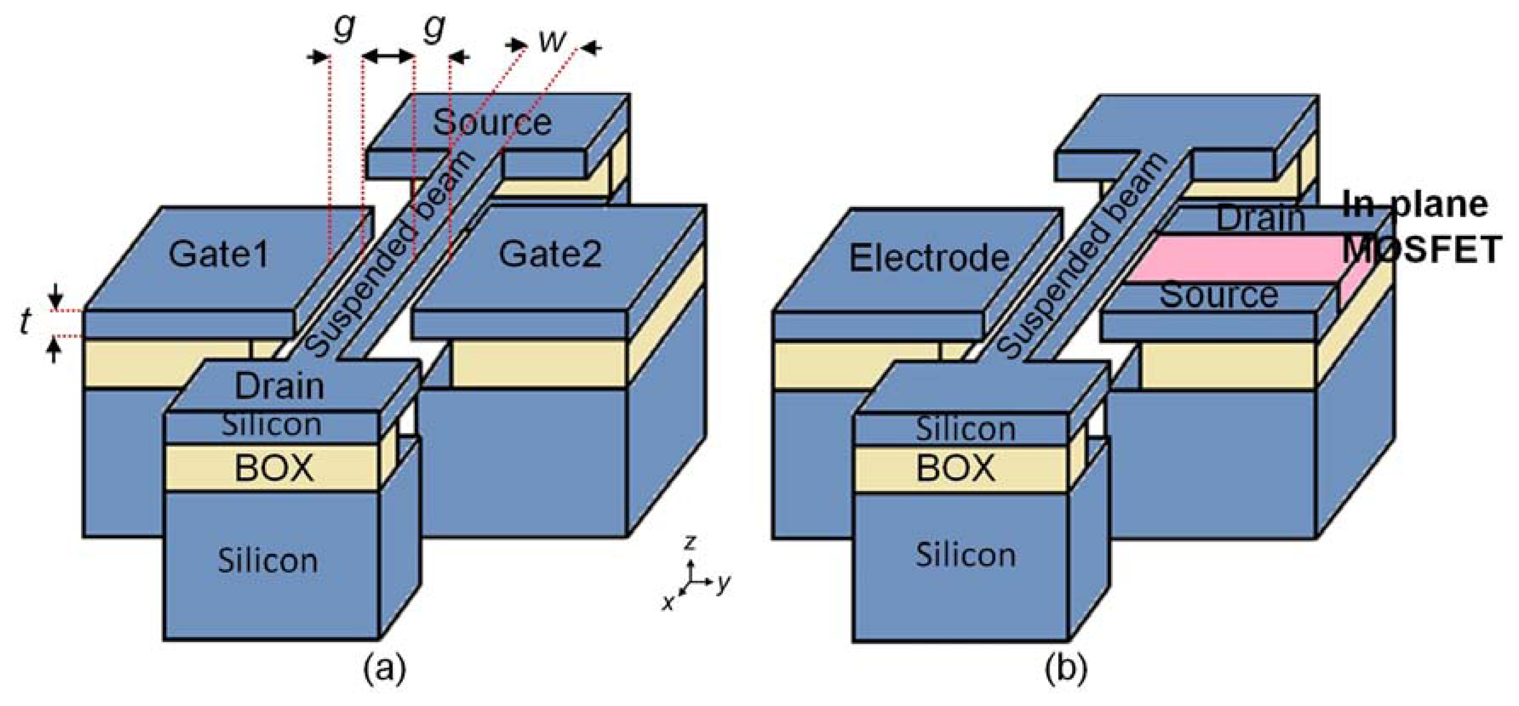
The IP R-NEM sensor consists of a suspended clamped-clamped (CC) beam and two side electrodes (Figure 1a). The sensor is fabricated based on SOI technology considering the uniform doping for the whole structure. The suspended beam is later considered as the laterally resonating channel for the JL FET. The CC beam is excited by an alternating current (AC) voltage due to the equality of its resonant frequency with the frequency of the AC voltage. The changes in the displacement of the CC beam cause changes in the current of the JL FET that is used for the detection of the resonance frequency. This is one possible detection method for the sensor besides the capacitance detection method. For the second sensor, an in-plane MOSFET is integrated with the suspended beam, IP RSG-FET sensor (Figure 1b). In this structure, the beam acts as the suspended gate for the MOSFET that moves laterally and induces current in the channel of the MOSFET. In both sensors, the adsorbed linker and target molecules on the surface of the beam changes its resonance frequency and as a result causes variation in the current of JL FET or MOSFET.
2.1. Analytical Calculations
The resonance frequency of the first lateral mode of the clamped-clamped beam is calculated by [9–11]:
In order to operate the NEM sensor with a safe margin, Vdc will be chosen to be well below the pull-in voltage and assumed that kb ≈ kbm and consequently fr ≈ f0.
Energy is dissipated from the resonator by different damping mechanisms. In general, the energy in the resonator is dissipated via the ambient, QAmbient (gas/liquid damping), through the anchors, QAnchor (anchor damping/loss), and its material itself, QThermoelastic (thermoelastic damping) [16]. QTotal is defined as the ratio of the total energy stored in the system to the energy dissipated or lost per cycle of vibration and is calculated as follows [16]:
QAmbient, is calculated by [17]:
The damping factor, b, is calculated as follows [18,19]:
The inverse quality factor due to the thermoelastic damping, , for dimensions down to nano-scale and the temperature above 100 K is calculated by [23]:
The anchor damping for nano-scale resonators in [24] is defined due to the tunneling of phonons between the beam and its anchors, which is calculated by [24]:
However, the anchor damping, QAnchor, in [25] is derived based on a two dimensional elastic theory as follows:
The parameters used for the calculation of QTotal and other key parameters such as resonant frequency, mass, and spring stiffness for the sensors are shown in Table 1. We assume sensors work at atmosphere and temperature of 300 K. QAnchor-phonon was not considered for the calculation of QTotal for the sensor as it was a few orders of magnitude larger than other components of QTotal and did not limit the total quality factor. As shown in Table 1, first QAmbient and then QAnchor are smaller than QThermoelastic and restrict QTotal. By using the vacuum and low temperature for working condition of the resonator, QAmbient and QThermoelastic will be reduced respectively and QAnchor plays the dominant role among the damping sources. The anchor damping can be reduced to zero by properly designing the sensor using a free-free beam. The details of this concept will be presented elsewhere.
2.2. Numerical Analysis
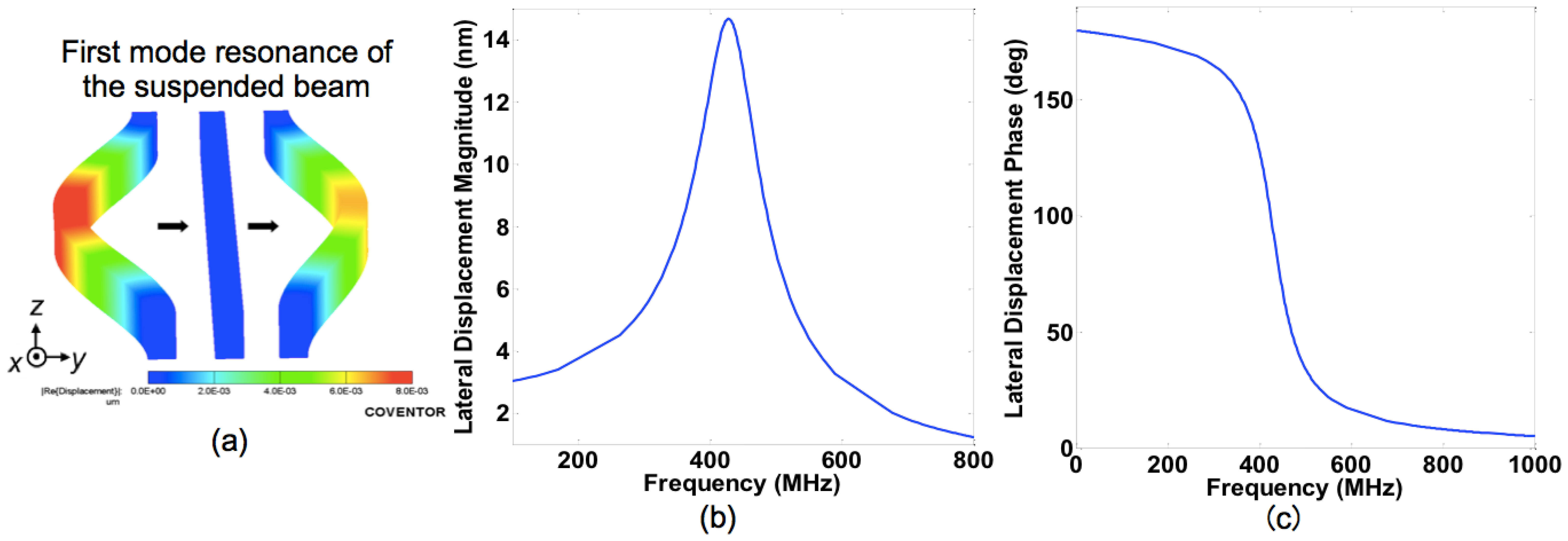
CoventorWare [27], was used for simulating the NEM sensors. This suite consists of a three dimensional finite-element-method (3D FEM) part including Designer and Analyzer and a circuit-level module, Architect. First, we conducted the 3D FEM analysis for the IP R-NEM sensor. Then, one of the electrodes in the IP R-NEM sensor was substituted with a lateral MOSFET in circuit-level modeling using Architect to realize the IP RSG-FET sensor. The first in-plane mode of the beam is obtained by using Analyzer at the frequency of 432.77 MHz as shown in Figure 2a. The magnitude and phase of the in-plane displacement versus frequency for the beam in the presence of a sinusoidal pressure load with the magnitude of 1 kPa are shown in Figure 2b,c, respectively. When the frequency of the applied pressure is equal to the resonance frequency of the beam, it resonates and shows a large peak for the displacement at the resonance frequency as shown in Figure 2b. Figure 2c shows also a change of 180 deg for the displacement of the beam at the resonance frequency. The derived numerical values including the resonance frequency, damping factor and quality factors are shown in Table 2, which are consistent with the analytical values in Table 1.
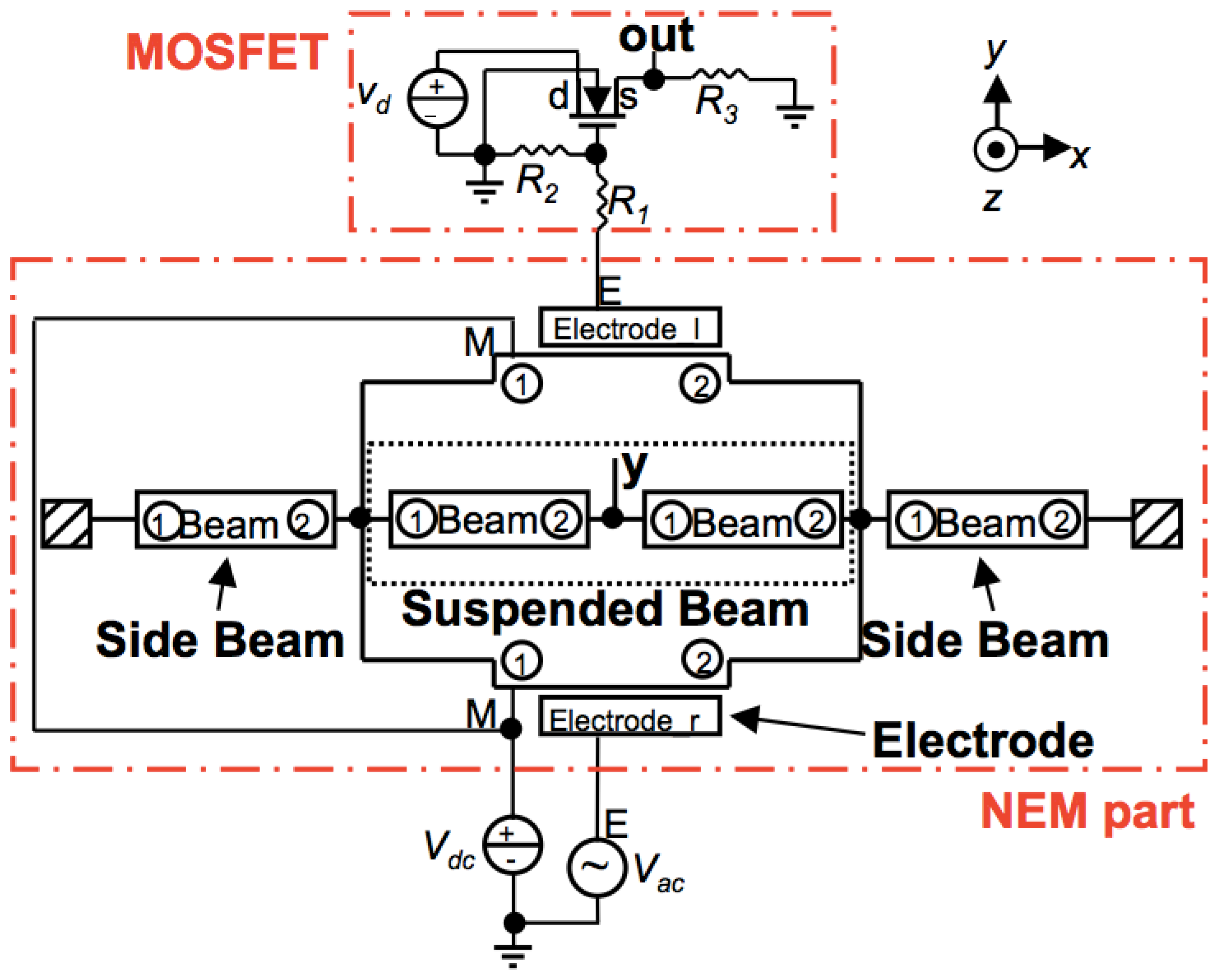
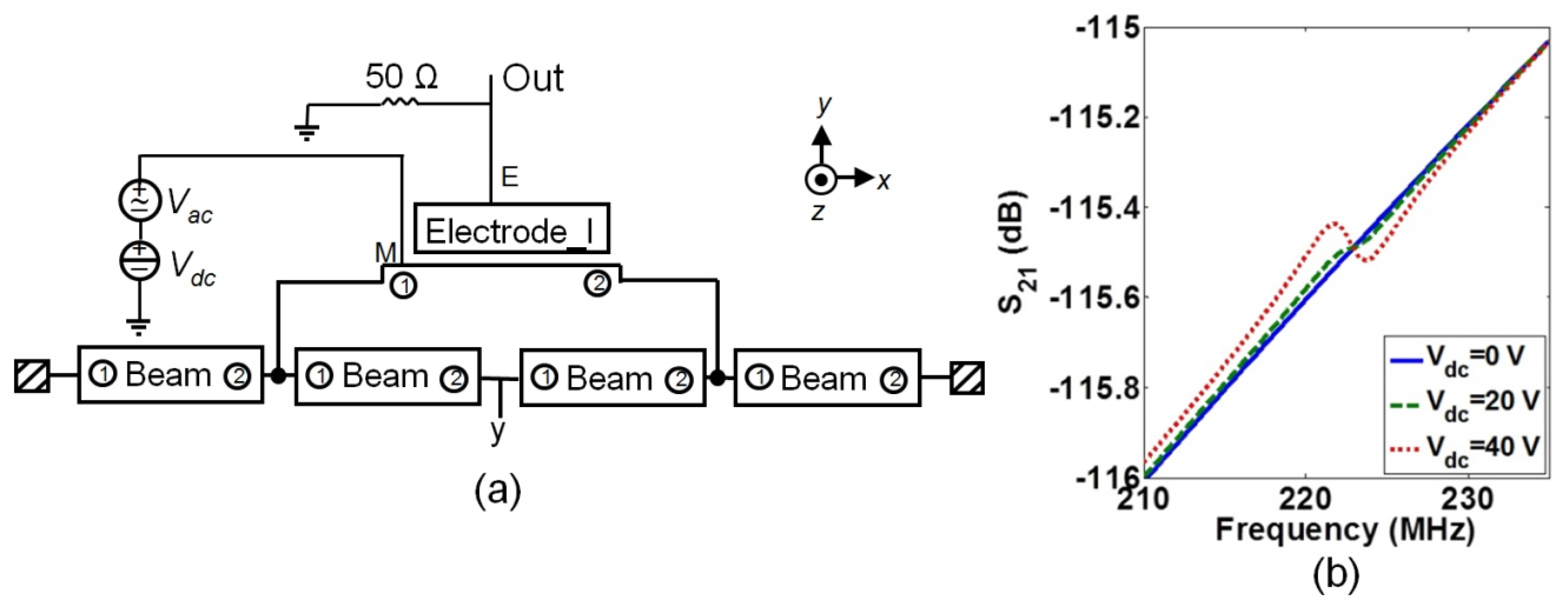
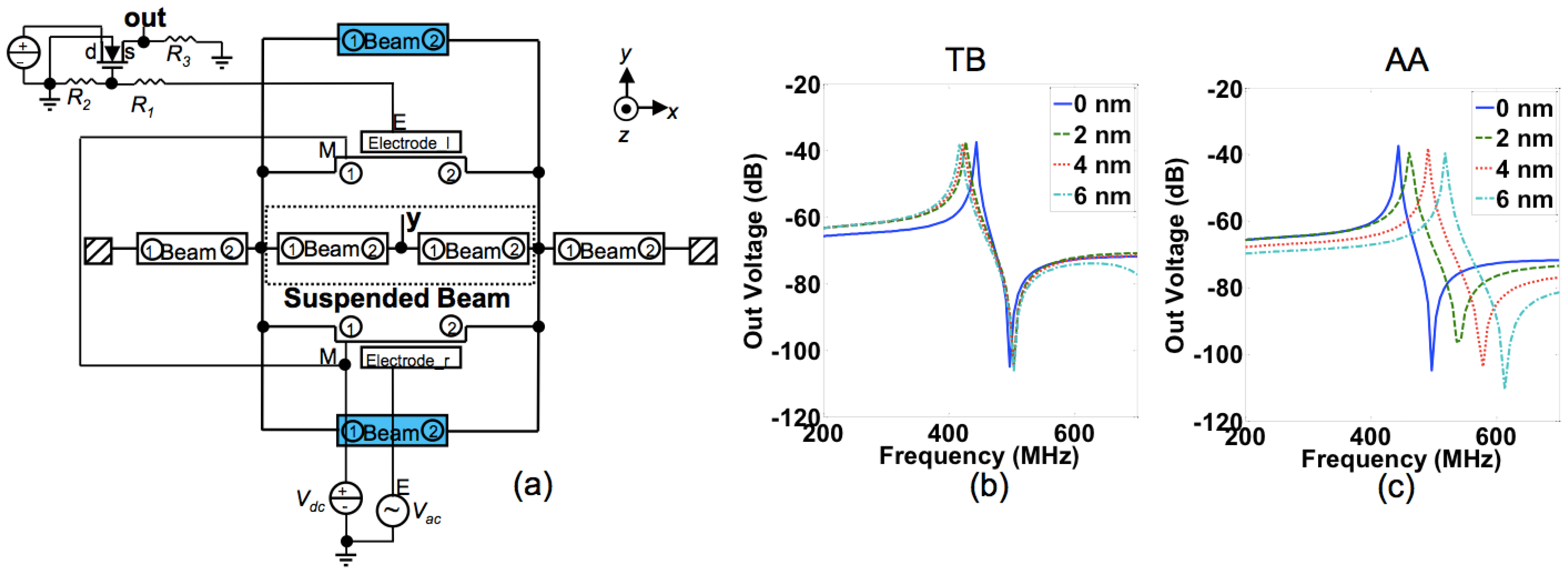
Architect was used to prepare a hybrid NEM-MOS circuit model to analyze the IP RSG-FET sensor. The hybrid circuit model in Figure 3 consists of a NEM part (a suspended beam and side electrodes) and a MOSFET. The suspended beam is modeled using two central beam components, to model the node at the center, with two side beam components to avoid the existing limitations of the software. A DC voltage is applied to the beam and an AC voltage is applied to the side electrode for biasing. The node ‘out’ in Figure 3 denotes the output voltage of the sensor. The values for resistance, R1 and R2, in this model were chosen with the smallest possible value to ensure the sensor resonance behavior remains valid. The n-type MOSFET has the 1 μm-channel length, which is the same as the length of the beam.
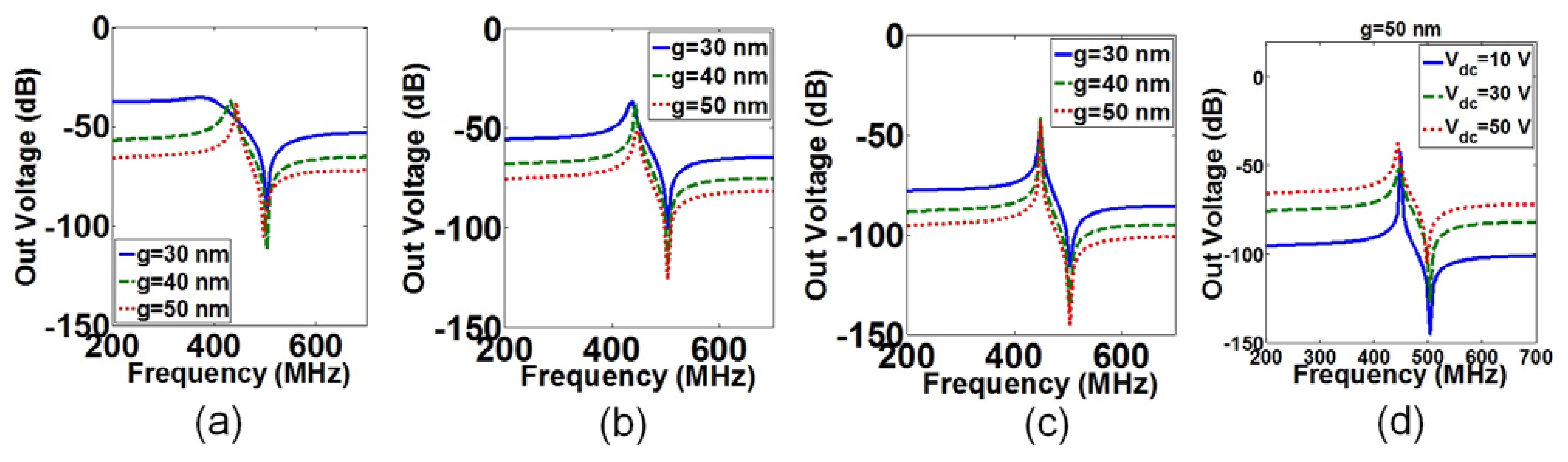
The gap was changed from 50 to 30 nm for three different DC voltages in order to investigate the effects of gap changes on the resonance frequency. The output voltage versus frequency for different gaps and voltages are shown in Figure 4, in which the left peaks present the resonance frequency while the right peaks denote the anti-resonance frequency [26]. Figure 4a shows that the resonance frequency shifts to lower frequencies by decreasing the gap at Vdc = 50 V. This is due to the fact that by reducing the gap, kbe in Equation (5) increases and results in smaller kb with respect to Equation (4) and consequently lower fr based on Equation (6). For Vdc = 30 V in Figure 4b, this effect is only visible when the gap reduced from 40 nm to 30 nm. By reducing the gap at Vdc = 10 V in Figure 4c, there will not be a shift for the resonance frequency as the effect of kbe on kb is smaller for smaller Vdc. Figure 4a–c shows that the widening of the resonance frequency spectrum is larger by reducing the gap in different voltages, which means a smaller QTotal. This fact is explained by the dominant effect of QAmbient in these results, since it was assumed that the sensor works in the atmosphere and at room temperature. By reducing the gap with respect to Equation (9), the damping factor increases and results in smaller QAmbient due to Equation (8). The output voltage versus the resonance frequency for g = 50 nm at Vdc = 10 V to 50 V are shown in Figure 4d. Figure 4d shows that by increasing Vdc from 10 V to 50 V, the resonance frequency decreased due to increasing of kbe in Equation (5) and causes reduction in kb and consequently reduction in the resonance frequency with respect to Equation (4). The reduction of the resonance frequency with increasing of Vdc is called spring softening [14]. Reduction in kb causes smaller QAmbient and wider resonance frequency spectrum similar to Figure 4a–c.
3. Sensing Process of Nano-Electro-Mechanical (NEM) Sensors
The sensing process of NEM sensors consists of two steps of functionalization and detection processes. The selective detection of particular biological or chemical molecules are possible by the functionalization of the surface of the suspended beam using various self-assembled monolayer (SAM) linker molecules, such as Amino-propyltrimethoxysilane (APTES) as a silane coupler, or alkene/alkyne-based molecules.
3.1. Analytical Calculations
Linker molecules are supposed to coat the surface homogeneously, for this reason, we have modeled these molecules simply by adding an extra surface coating layer onto the suspended beam. The surface functionalization processes are performed in reality either in liquid or in vapor that result in different surface coating configurations. We studied three coating configurations: top and bottom (TB), only top (OT) and all-around (AA) coating. For the TB configuration in Figure 5a two surface layers with the same thickness are considered on the top and bottom of the beam. This configuration is the suitable model to describe the coating in liquid as the molecular solution flows more freely above and under the beam rather than through the nano-scale gap between the suspended beam and the electrodes. We also considered the OT configuration (Figure 5b) for the case that the gap underneath the suspended beam is as small as the side gaps. The AA configuration shown in Figure 5c is also a likely case for the coating in vapor, as the vapor flow can go through narrow gaps more easily than the liquid flow. This configuration may also be applicable for the liquid phase if the side and bottom gaps are wide enough so the solution reaches all surfaces of the suspended beam easily. The total mechanical spring stiffness for the TB configuration, kb-TB, is given by [7]:
Equations (19–22) show both spring stiffness and mass will increase by increasing the thickness of the coating layer and affects the resonance frequency. To find out the dominant factor between them, the changing rates of mass, (Δmbl/mb), and spring stiffness, (Δkbl/kb), were considered as representative parameters in Table 3. Here Δmbl and Δkbl are changes of the mass and spring stiffness due to the linker molecules and a 1 nm-thick coating layer is used as an example for the calculations. Table 3 shows that by increasing the thickness of the coating layer in both OT and TB configurations the increase of mass is higher than that of the spring stiffness while for the AA configuration the spring stiffness plays the dominant role. According to the dominant parameter for each configuration in Table 3, the changes in resonance frequency, Δf0, will be positive or negative by considering Equation (1). Note that, Δf0 > 0 shows the increase in f0 by increasing the thickness of the coating layer in the AA configuration, while Δf0 < 0 presents the reduction of f0 by increasing the thickness of the coating layer in the OT and TB configurations. This effect is also validated using the simulation later. Previous studies [28,29] on micro-resonators, show that the deposition of coating materials and adsorption of an analyte can affect not only the mass but also the spring stiffness. This effect results in a change in the resonance frequency towards higher or lower values.
In order to model the sparse and random adsorption of target molecules to the functionalized surface we simply increased the density of the coating layer with various configurations because the target molecules will change the effective mass of the beam without much affecting the spring stiffness of the beam. By using this method, we are able to study the impact of solely the mass increase due to the adsorbed target molecules on the resonant frequency and evaluate the mass responsivity of the sensor for the detection process. The numerical analysis for the mass responsivity is given in the next section. Using Equation (6), the mass responsivity, S, is calculated as follows [30]:
By using the values in Table 1, S is calculated and equal to 0.007 zepto g/Hz, which is then compared with the numerical value in the next section. Considering several noise processes in the operation of a resonator, the changes of the mass due to the adsorbed molecules, Δmba, is calculated as follows [31]:
3.2. Numerical Analysis
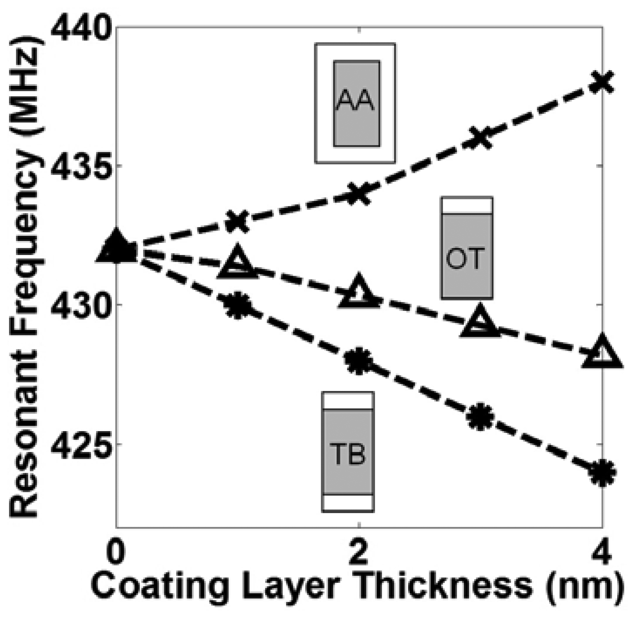
Various insulator/polymer materials were used for modeling the functionalization process of the IP R-NEM sensor by adding a coating layer in different configurations in Designer to realize a homogenous and dense SAM layer in reality. We assumed for the present 3D FEM simulation that both ends of the coating layer were not anchored. This assumption may cause some differences from the results of the analytical model in Table 3, which assume the coating layer was also doubly clamped. In reality, it depends on the details of the surface coating of the resonator at the clamping points whether or not the non-anchored model is more appropriate. Figure 6 shows the resonance frequency versus the coating layer thickness for the TB, OT and AA configurations. In Figure 6, the frequency decreases in the TB and OT configurations by increasing the coating layer thickness. This trend shows the dominant effect of mass on the resonance frequency, which is consistent with the results in Table 3. Change in the resonance frequency is lower for the OT configuration than the TB configuration, due to its smaller mass value of the coating layer. Higher resonance frequencies for the OT configuration are explained by the smaller mass of the coating layer for the OT configuration than that of the TB configuration. On the contrary, the resonance frequency increases by increasing the coating layer thickness in Figure 6, as expected from Table 3 because of the dominant effect of the spring stiffness enhancement for the AA configuration.
To study the impact of adding the coating layer on the output voltage of the designed IP RSG-FET sensor, we introduced the coating layer onto the beam in our circuit model by adding extra beam components as shown in Figure 7a. The same assumption of non-anchored ends for the coating layer is also applied here. Figure 7b,c shows the output voltage versus frequency calculated with different coating layer thicknesses of the TB and AA configurations. The frequency spectra of the output voltage shift to low frequencies by increasing the thickness of the coating layer for the TB configuration (Figure 7b) while the trend is reverse for the AA configuration (Figure 7c). These results show the effect of the mass change is dominant for the TB configuration and the effect of the spring stiffness change is dominant for the AA configuration as explained previously in this section. These results are consistent with the previous 3D simulation results in Figure 6.
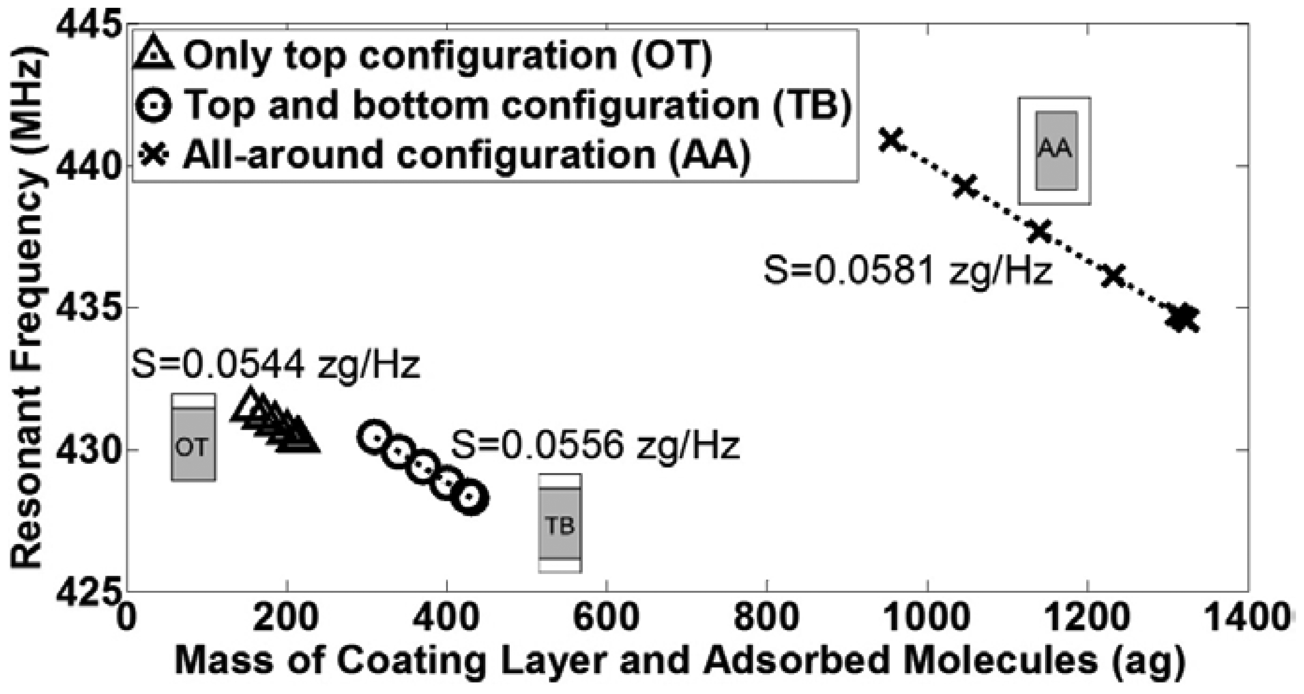
The density of the added coating layer in different configurations for the functionalization process has been increased to model the adsorbed target molecules for the detection process. The resonant frequency for all coating configurations versus the total mass of the surface coating layer (2 nm-thick) and the adsorbed target molecules are shown in Figure 8. Regardless of the different coating schemes, the increase in the mass due to the adsorbed molecules decreases the resonant frequency linearly. The inverse slope of the resonant frequency versus mass shows the mass responsivity, S. Figure 8 shows virtually the same S values of 0.05 zeptogram/Hz for all configurations regardless of modified resonant frequency with different functionalization schemes and independent of the surface area of the beam that is used for adsorption. The calculated numerical value for S is one order of magnitude larger than the calculated analytical value in the previous section. This fact can be explained due to the assumption of non-anchored coating layer as well as the difference between the analytical and numerical values for the resonance frequency.
A few of the most recent research works on mass detection based NEM sensors using a CC beam with different materials [4,12,30,32,33], are given in Table 4. The proposed NEM sensors in this paper show higher sensitivity than that of the stated sensors in Table 4.
4. Fabrication of Nano-Electro-Mechanical (NEM) Sensors
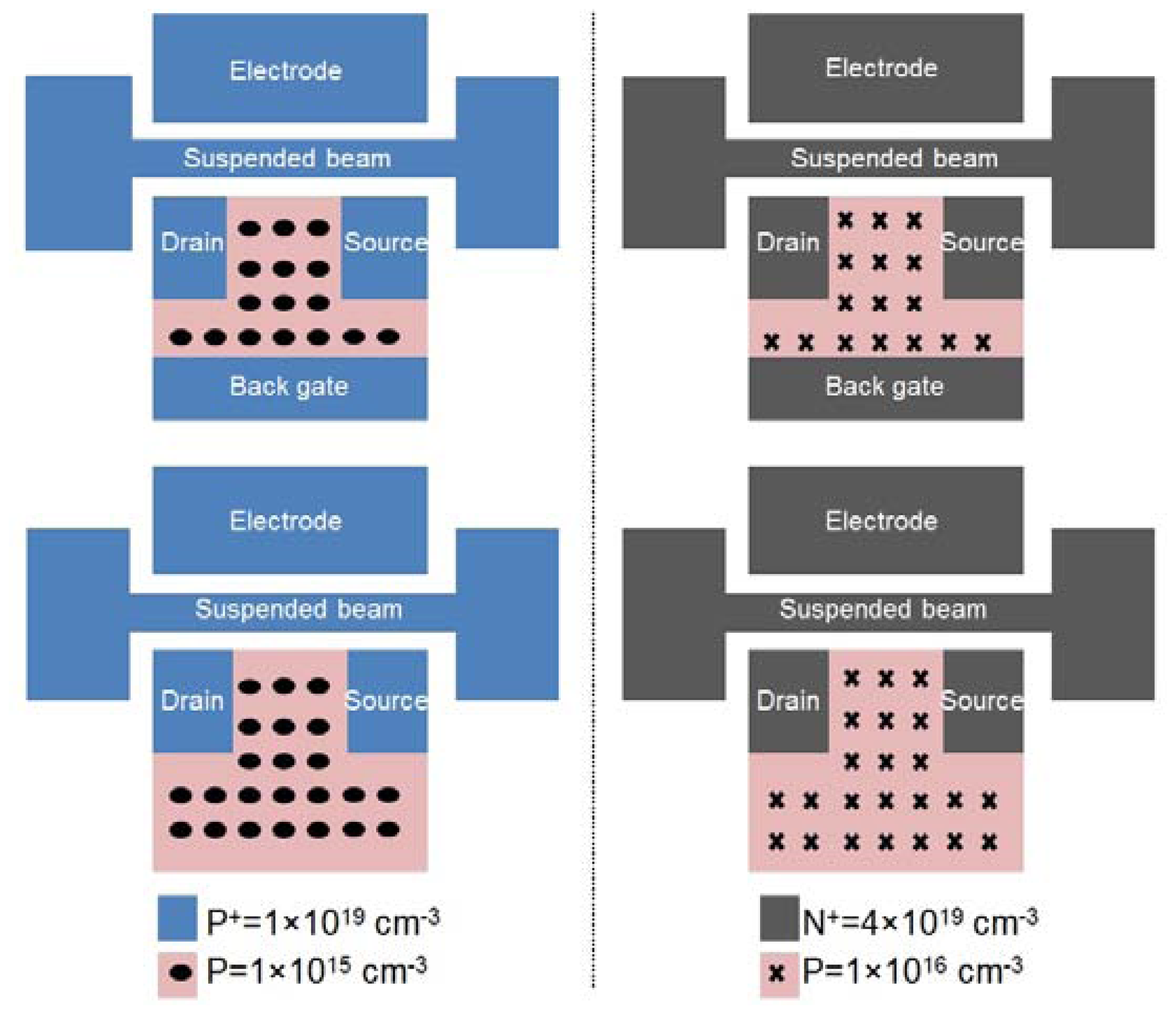
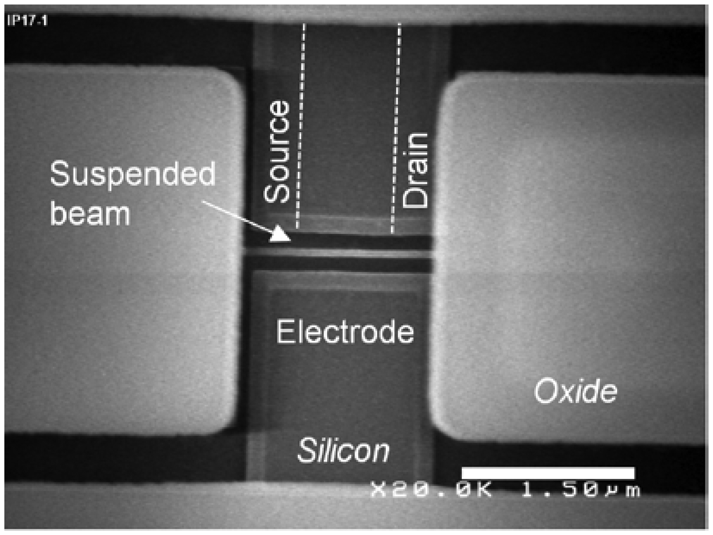
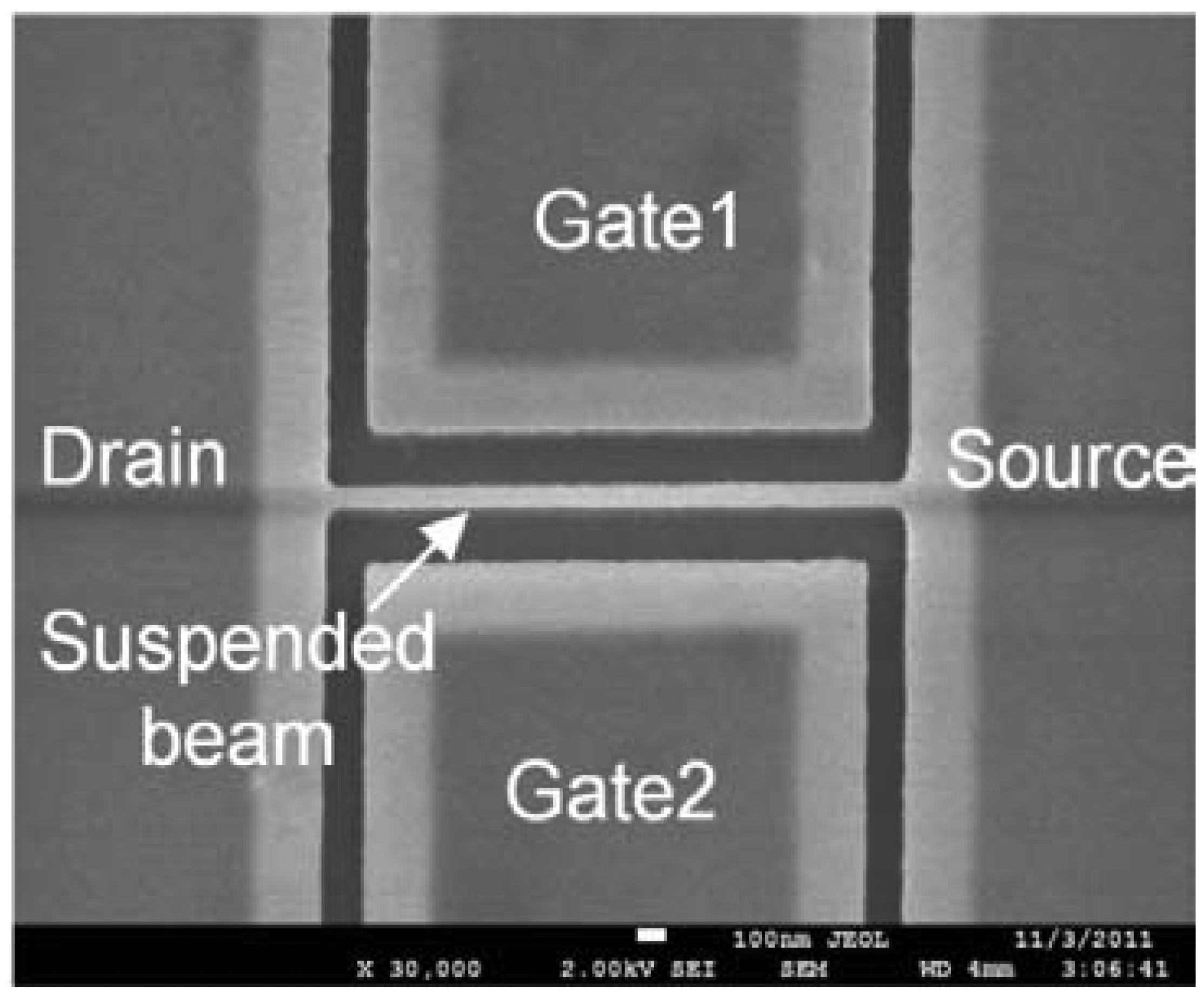
The IP R-NEM sensor was fabricated on an SOI platform. The thickness of the SOI and buried oxide (BOX) layers for this sensor are 40 nm and 145 nm, respectively. P-type doping of P = 1015 cm−3 is considered for the SOI wafer. First, the SOI wafer was implanted with the doping of P+ = 1019 cm−3. Then the heavily-doped silicon was patterned and the beam was released using vapor hydrofluoric (HF). A 15 nm-layer of thermal oxide was grown on the surface of the patterned silicon, especially around the suspended beam for passivation and minimizing of the silicon surface states [34]. After that, poly silicon was deposited to fill the etched area around the beam to protect the beam from further processing steps. Contact holes above the silicon pads are opened by etching poly silicon with the etch stop layer of thermal oxide. Then, oxide is deposited and contact holes are patterned in this layer. Aluminium (Al) is deposited and patterned for contact pads and wiring afterwards. Finally, a window is opened in oxide and poly silicon above the beam for the suspension of the beam using xenon difluoride (XeF2). The scanning electron microscope (SEM) image of the sensor is shown in Figure 9. The same fabrication steps of the IP R-NEM sensor applied for the IP RSG-FET sensor except considering two values of p-type doping, P = 1015 cm−3 and P = 1016 cm−3, for the SOI wafers. Moreover, during the implantation steps with different dopings of P+ = 1019 cm−3 and N+ = 4 × 1019 cm−3, the channels of the MOSFETs were protected by resist. The top view schematics in Figure 10 show the doping strategies for IP RSG-FET sensors. The SEM view of the sensor is shown in Figure 11.
5. Direct Current (DC) and High Frequency Characterization of Nano-Electro-Mechanical (NEM) Sensors
The detection of resonance frequency is the bottleneck of nano-electro-mechanical (NEM) resonators due to the need of good signal to noise/background ratio (SNR/SBR) to single out very small output signals [35]. For this reason, several high frequency techniques were applied for the NEM sensors to investigate the best resonance frequency detection method for the sensors with the current designs.
5.1. Characterization of In-Plane Resonant Nano-Electro-Mechanical (IP R-NEM) Sensor
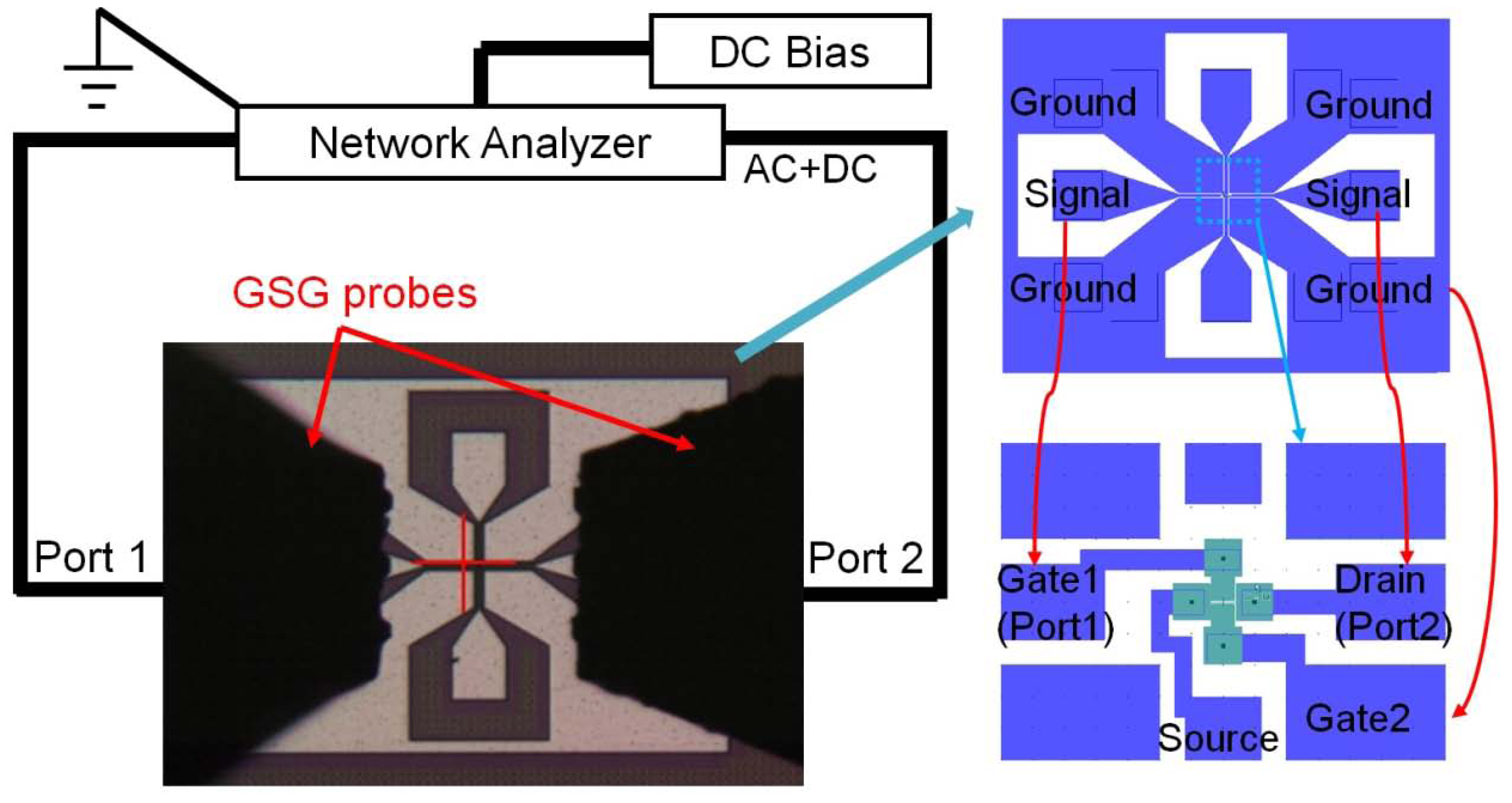
For the radio frequency (RF) characterization of the IP R-NEM sensor, Cascade SUMMIT 12000B probe station was used. The S-parameters for the sensor were measured using an Agilent E8361A PNA network analyzer. Ground-signal-ground (GSG) probes with the pitch of 150 μm were used for the measurement. The characterization setup is shown in Figure 12. The two-port calibration was done at the end of GSG probes. The RF characterization was done for the beam with w = 135 nm, g = 80 nm and l = 2,000 nm that has a resonance frequency of 285 MHz based on the numerical analysis. The AC voltage with the power of −10 dBmWatt, IF bandwidth of 500 Hz and number of point of 601 were applied. The DC voltage is applied to the beam using the Agilent semiconductor device analyzer B1500. The measurement was done in the atmosphere and at room temperature.
It was not easy to distinguish the resonance peak in the transmission signal, S21, from the background noise signal for this device. In order to explain this effect, the IP R-NEM sensor with the current dimensions is compared to the 14-MHz in-plane NEM resonator by Durand et al. [36]. Their resonator consists of a vibrating gate and a resonant suspended gate MOSFET (RSG-MOSFET) that is fabricated using silicon-on-nothing (SON) technology. The vibrating gate has the dimensions of w = 165 nm, t = 400 nm, g = 120 nm and l = 10 μm and measured parameters for the RSG-MOSFET resonator are: f0 = 14.43 MHz, Rx = 736 kΩ and QTotal = 700. The electrical setup for the capacitive detection of the RSG-MOSFET resonator is similar to the setup for the IP R-NEM sensor in Figure 12 and it showed 2 dB-magnitude peak for the transmission signal. The Rx for the IP R-NEM sensor that works in the atmosphere is 100 times higher than that of the RSG-MOSFET using Equation (16). Due to this fact, the IP R-NEM sensor shows higher signal drop across the resistance and consequently smaller output signal than the 2 dB-magnitude transmission signal of the capacitive detection for the RSG-MOSFET. This reason explains the difficulty in distinguishing the resonance peak with very small magnitude from the back ground noise signal.
The circuit-level simulation of an IP R-NEM sensor with one side electrode in Figure 13a was done to confirm the previous comparison between the IP R-NEM sensor and RSG-MOSFET. Figure 13b shows the very small magnitude of S21 in the presence of different applied Vdc that is consistent with our previous explanation. In order to reduce Rx and improve the transmission signal for the sensor, the measurement should be done in high vacuum, same as the RSG-MOSFET. It is important to note, that the lower working pressure reduces Rx if QTotal is mainly dominated by air damping, QAmbient. For example, QTotal for the NEM sensor with w = 135 nm and l = 2,000 nm is dominated by anchor doping, QAnchor, and its Rx is not reduced much by using high vacuum. Use of different measurement techniques such as lock-in measurement [37–39], is a good option for the measurement of these devices.
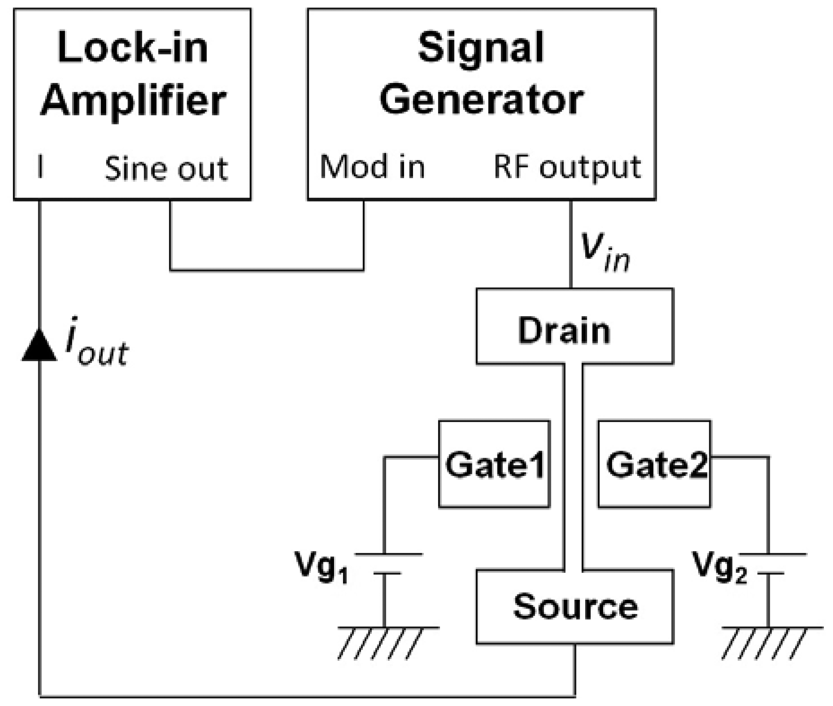
We have applied a down-mixing technique [40,41] for the RF characterization of the IP R-NEM sensor due to the above mentioned difficulties in the RF characterization of the sensor using a network analyzer. This current technique takes advantage of the intrinsic gain of the integrated JL transistor [42] within the IP R-NEM sensor. The measurement setup is shown in Figure 14.
By applying different voltage to gates, Vg1 and Vg2, the strongest current modulation due to the movement of the beam will be achieved. The signal generator in Figure 14 was used to apply a frequency modulation carrier signal, vin, to drain. The measurements were done at high vacuum (10−6 mbar) and room temperature. The lock-in amplifier was used to detect the output current signal, iout, from source. The output current, iout, is defined by [40]:
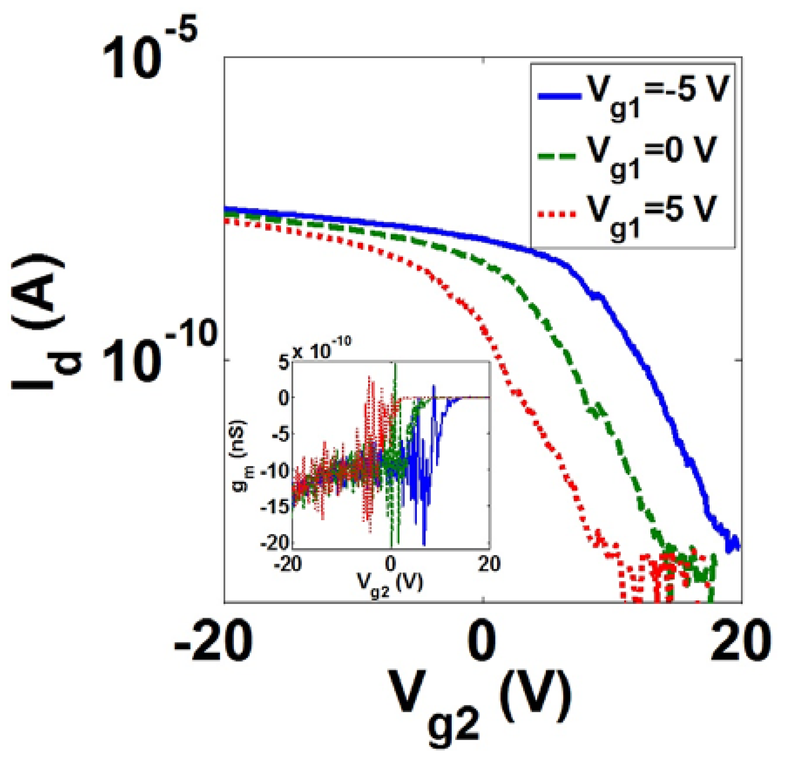
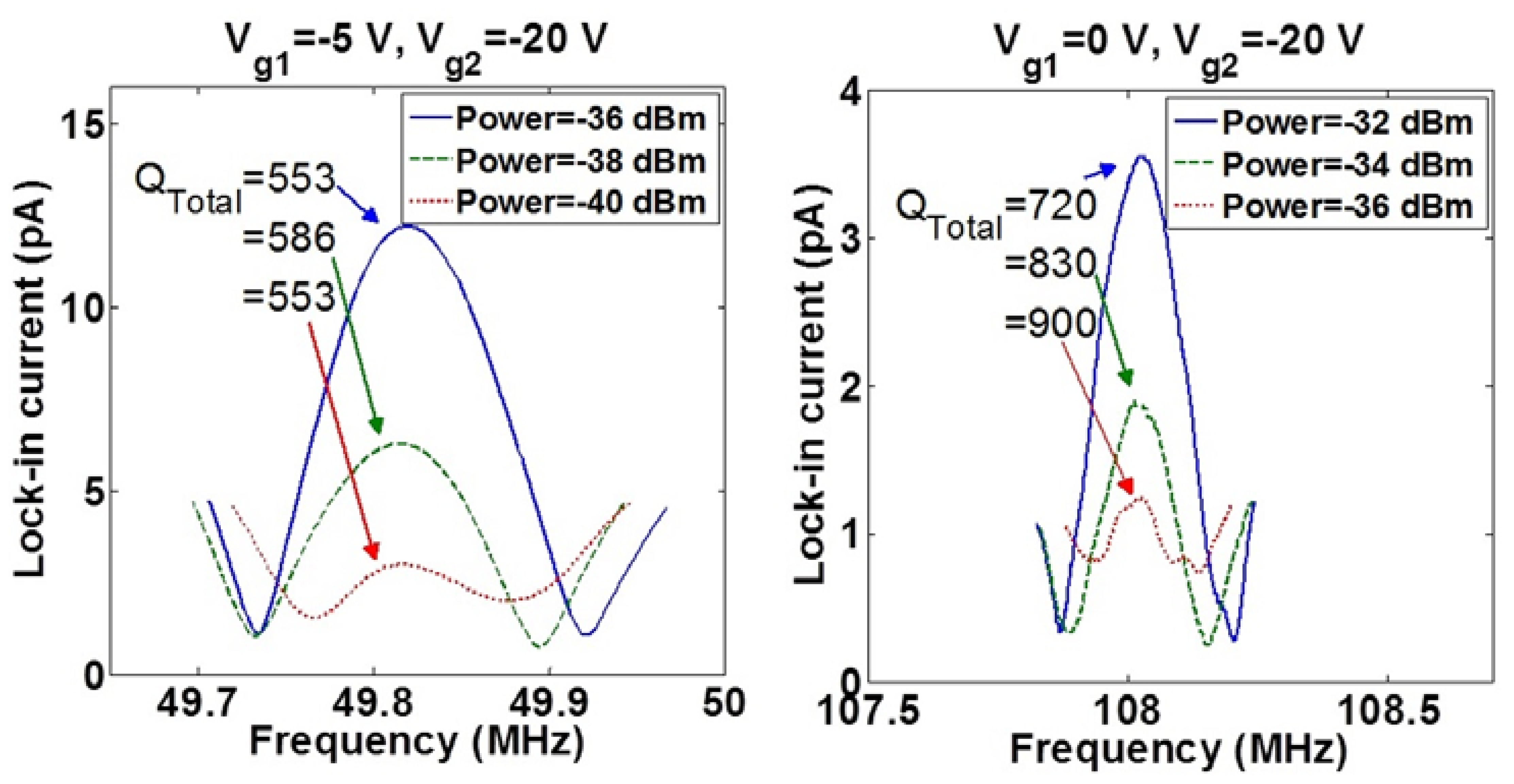
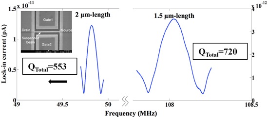
Figure 15 shows the impact of applying different voltages to gates of the sensor l = 1.5 μm, w = 45 nm and t = 40 nm on its Id-Vg and gm-Vg (inset of Figure 15) characteristics. The asymmetrical applied voltages of Vg1 = −20 V and Vg2 = −5 V provides higher ON-current as well as high gm.
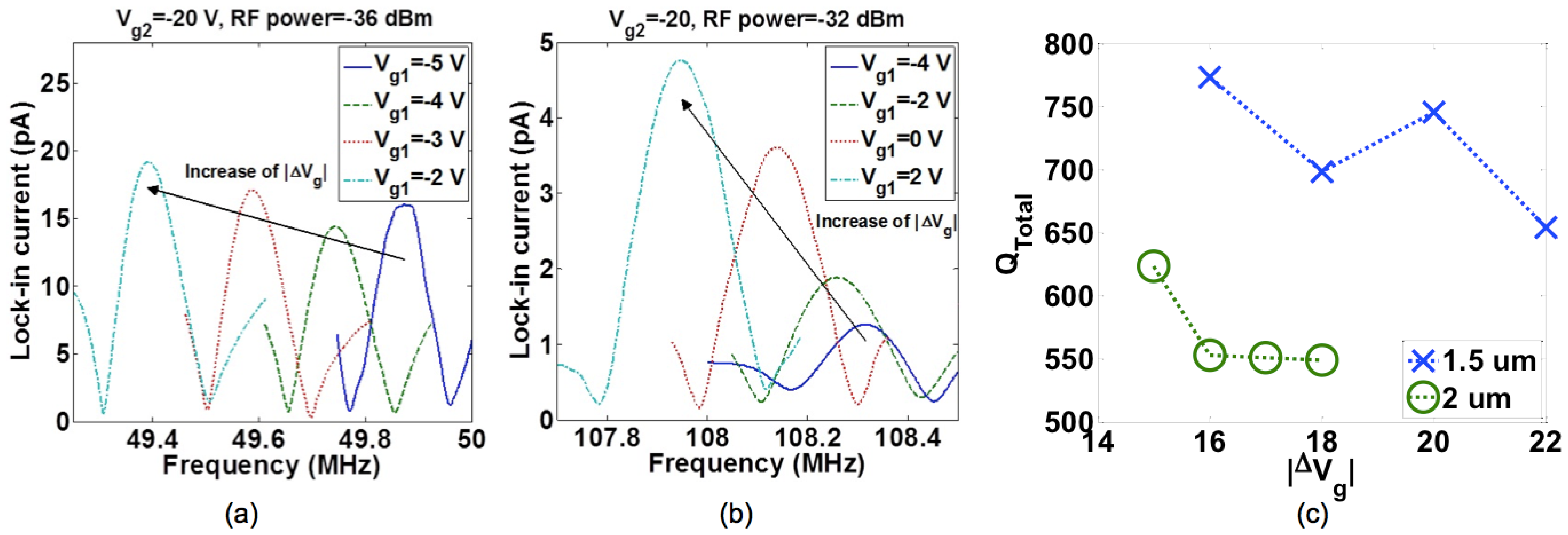
The lock-in current versus frequency of two sensors with l = 1.5 and 2 μm are shown in Figure 16. The measured f0 and QTotal are less than the analytical values of f0 = 158.98 MHz and QTotal = 9,762 for l = 1.5 μm and f0 = 89.42 MHz and QTotal = 23,141 for l = 2 μm considering a 15 nm-silicon dioxide (SiO2) layer around the beam. These differences can be explained due to changes of dimensions of the suspended beam from the original designed values. In order to investigate the impact of gates' bias voltages on the resonance frequency, Vg2 was fixed to −20 V while Vg1 was changed. The lock-in current of both sensors versus frequency characteristics by changing Vg1 are shown in Figure 17a,b. In both devices, an increase in |ΔVg = Vg2 − Vg1| causes an increase in the electrical spring stiffness and reduces the total spring stiffness, which leads to the reduction of the resonance frequency so called softening effect. The QTotal of both sensors versus |ΔVg| are shown in Figure 17c. The reduction of QTotal by increasing |ΔVg| can be seen for both sensors especially for the shorter length beam due to the higher applied voltages. The lock-in current versus the frequency of resonators for various RF powers are shown in Figure 18. This figure shows the stability of the resonance frequency of sensors by increasing the RF power. However, the 2 μm length sensor shows the reduction of QTotal by increasing the RF power. This is due to the fact that by increasing the power, the temperature of the beam and consequently QThermoelastic will increase. Higher value for QThermoelastic leads to the dominancy of this factor in the total quality factor and the reduction of QTotal with respect to Equation (7). The dependence of the resonance frequency of the resonator to the value of applied RF power and |ΔVg| shows the necessity of doing the measurement at low temperatures. The reason for the increasing temperature in the beam may be explained by the existence of the thermal oxide layer around the beam. This is due to the fact that oxide has smaller thermal conductivity in comparison with silicon, which results in less dissipation of heat to the environment. For this reason, the fabrication of a suspended beam without thermal oxide will improve this temperature dependency. Applying the same measurement technique for the functionalized sensor will be done in the future.
5.2. Characterization of In-plane Resonant Suspended Gate Field-Effect-Transistor (IP RSG-FET) Sensor
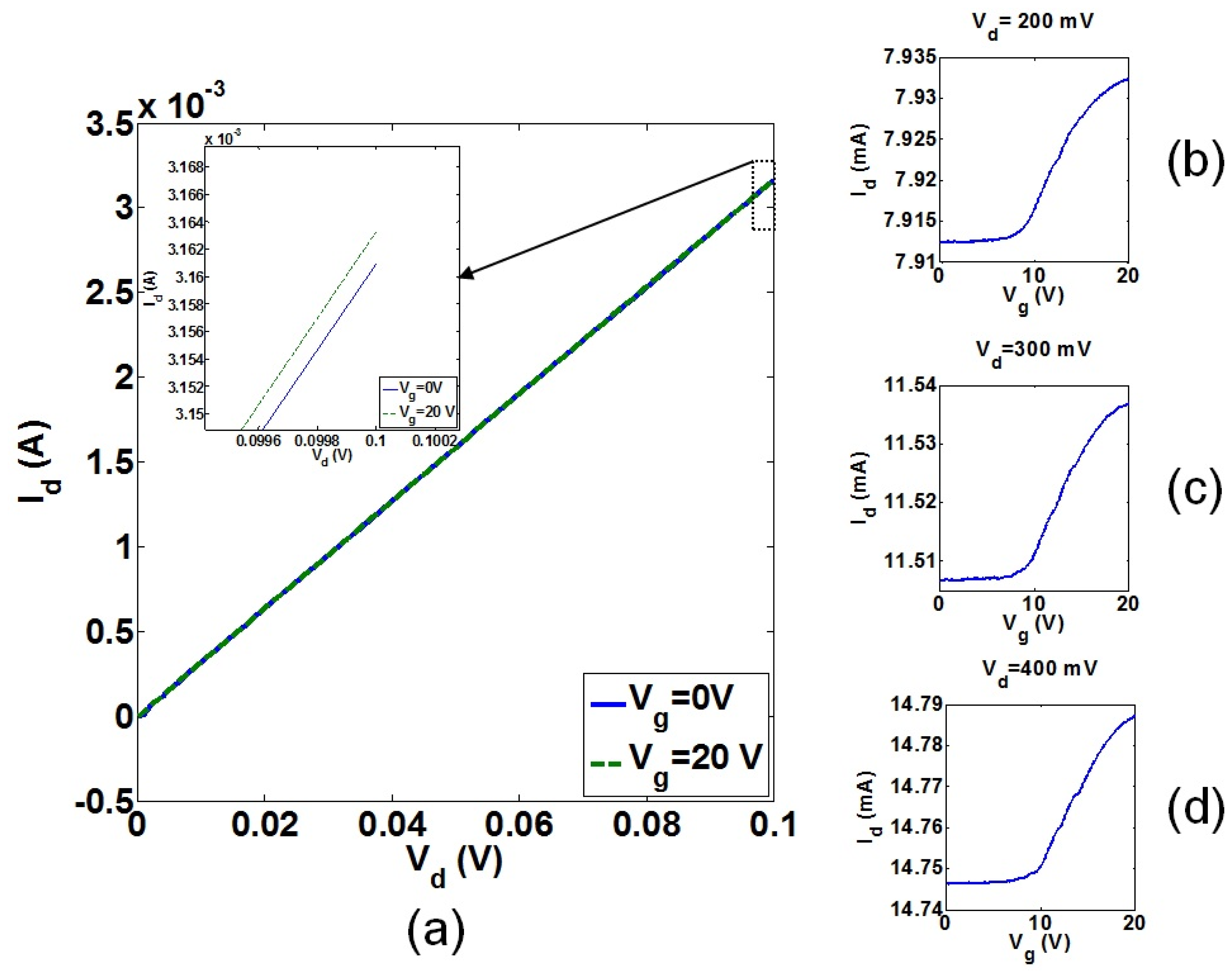
As discussed before, a MOSFET is integrated with the beam for the IP RSG-FET sensor to improve the magnitude of the transmission signal in which the output signal from the NEM structure is amplified by the intrinsic gain of MOSFET [26,36], gm × ro, where ro is the output resistance of MOSFET. Similar to JL FET detection method for the IP R-NEM sensor, by optimizing the applied bias voltages in DC characteristics of the MOSFET, the maximum value for gm is achieved that amplifies the output signal of the MOSFET as much as possible. Based on the fabrication technology, after the implantation and drive-in steps for dopants, there is an estimated lateral diffusion length of 100 nm. The voltage of 0–0.1 V was applied to drain, Vd, for the enhancement-mode n-channel MOSFET (N+/P/N+-type) with channel length, lC, of 1,250 nm, l = 2,000 nm, w = 135 nm and g = 80 nm. The drain current-drain voltage, Id-Vd, characteristics of the MOSFET with different applied voltages to the suspended beam, Vg = 0 and 20 V, are shown in Figure 19a. Figure 19a shows the very small control of gate over the channel. The drain current-gate voltage, Id-Vg, characteristics of the MOSFET is shown in Figure 19b–d for Vd in the range of 200 to 400 mV. Figure 19b–d show the OFF-current in the order of raA and a very small ON/OFF current ratio. The current in Figure 19b–d increases by increasing Vd, which shows the strong impact of drain over the channel. The threshold voltage, Vt, of 9 V in Figure 19b–d is much larger than the analytically calculated value of Vt = 1.75 V for the conventional long n-channel MOSFET. This difference in the threshold voltages cannot be explained due to the drain-induced-barrier-lowering (DIBL) effect which should cause the reduction in the threshold voltage [42]. The same order of OFF-current has been found also for the depletion-mode p-channel MOSFET (P+/P/P+-type) with the same dimensions of the n-channel MOSFET.
In order to investigate the origin of high OFF-current, the leakage of the n-channel MOSFET from source and drain to the back gate was measured. The leakage current was in the order of 10−4 A for both drain and source and 1 μm-distance of back gate from source and drain shows the dopants diffusion of source and drain towards the back gate is more than the previously stated 100 nm. The value of diffusion length that gives this level of leakage current was found by simulating the device in ATLAS 3D [44]. The simulation results showed that by considering the dopant diffusion of 400 nm and a negative charge of −1 × 1012 cm−3 in the interface of the oxide layer and silicon beam, the same Id-Vg characteristics for the MOSFET in Figure 19 will be achieved. In order to isolate the source and drain as much as possible, a trench is milled between them using focused ion beam (FIB), which improved the Id-Vg characteristics negligibly. Designing of MOSFETs with a longer channel length may be a solution to avoid the issue of high OFF-current in these sensors.
6. Conclusions
In this paper we have presented the design, simulation, fabrication and characterization of in-plane resonant nano-electro-mechanical (NEM) sensors. These sensors are based on the mass detection principle and can be used as a bio/chemical sensor. The proposed sensors were designed and simulated using both three dimensional finite-element-method (3D FEM) simulation and hybrid nano-electro-mechanical metal-oxide-semiconductor (NEM-MOS) circuit simulation. The surface of the suspended beam should be functionalized for adsorption of target molecules. The linker and target molecules of the sensing process have been modeled by adding extra layers to the beam in different configurations for investigating the extreme mass responsivity of 0.05 zepto g/Hz for the sensors. The in-plane resonant nano-electro-mechanical (IP R-NEM) and in-plane resonant suspended gate field-effect-transistor (IP RSG-FET) sensors were fabricated successfully. The radio frequency (RF) characterization of the IP R-NEM senor was investigated in different analytical and numerical levels to clarify the best characterization method for the sensors with current specifications. Down-mixing technique was successfully applied for the RF characterization of the IP R-NEM sensors as the suitable high frequency characterization technique. Due to the challenges of the newly proposed fabrication technology of the IP RSG-FET senor, some post processing and simulations were done to investigate and improve the direct current (DC) characteristic of this sensor. The numerical analysis shows the impact of the lateral diffusion of source/drain dopants and also the possible trapped charges in the surface of the vertical channel of the MOSFET on the DC characteristics of the sensor. Further post-processing and design optimization should be conducted to improve or avoid the discussed challenges for IP RSG-FET sensors.
Acknowledgments
This work is financially supported by EUFP7 project NEMSIC (Hybrid nano-electro-mechanical/integrated circuit systems for sensing and power management applications). The authors sincerely acknowledge Cecilia Dupré, and Eric Ollier (CEA-Léti), Dimitrios Tsamados (Synopsys), Adrian Mihai Ionescu and Sebastian T Bartsh (EPFL), Cornel Cobianu (Honywell Romania), Silvia Armini, and Vlamidir Cherman (IMEC-BE) for their invaluable contribution and discussion throughout the project.
Conflict of Interest
The authors declare no conflict of interest.
References
- Brand, O. Fabrication Technology. In Advanced Micro and Nanosystems; Brand, O., Fedder, G.K., Eds.; Wiley-VCH Verlag GmbH & Co. KGaA: Weinheim, Germany, 2005; Volume 2, pp. 1–67. [Google Scholar]
- Ollier, E.; Duraffourg, L.; Delaye, M.T.; Grange, H.; Deneuville, S.; Bernos, J.; Dianoux, R.; Marchi, F.; Renaud, D.; Baron, T.; et al. NEMS Devices for Accelerometers Compatible with Thin SOI Technology. Proceedings of 2nd IEEE International Conference of Nano/Micro Engineered and Molecular Systems, Bangkok, Thailand, 16–19 January 2007; pp. 180–185.
- Ollier, E.; Duraffourg, L.; Colinet, E.; Durand, C.; Renaud, D.; Royet, A.S.; Renaux, P.; Casset, F.; Robert, P. Lateral MOSFET Transistor with Movable Gate for NEMS Devices Compatible with In-IC Integration. Proceedings of 3rd IEEE International Conference of Nano/Micro Engineered and Molecular Systems, Sanya, China, 6–9 January 2008; pp. 764–769.
- Yang, Y.T.; Callegari, C.; Feng, X.L.; Ekinci, K.L.; Roukes, M.L. Zeptogram-scale nanomechanical mass sensing. Nano Lett. 2006, 6, 583–586. [Google Scholar]
- Hassani, F.A.; Cobianu, C.; Armini, S.; Petrescu, V.; Merken, P.; Tsamados, D.; Ionescu, A.M.; Tsuchiya, Y.; Mizuta, H. Design and Analysis of an In-Plane Resonant Nano-Electro-Mechanical Sensor for Sub-Attogram-Level Molecular Mass-Detection. Proceedings of International Conference of Solid State Devices and Materials, Sendai, Japan, 7–9 October 2009.
- Koumela, A.; Mercier, D.; Marcoux, C.; Purcell, S.T. Performances of Suspended Silicon Nanowire Resonators for Time Reference Applications. Proceedings of IEEE International Frequency Control Symposium, Baltimore, MD, USA, 21–24 May 2012; pp. 1–4.
- Hassani, F.A.; Cobianu, C.; Armini, S.; Petrescu, V.; Merken, P.; Tsamados, D.; Ionescu, A.M.; Tsuchiya, Y.; Mizuta, H. Numerical analysis of zeptogram/Hz-level mass responsivity for in-plane resonant nano-electro-mechanical sensors. Microelectron. Eng. 2011, 88, 2879–2884. [Google Scholar]
- Colinet, E.; Durand, C.; Duraffourg, L.; Audebert, P.; Dumas, G.; Casset, F.; Ollier, E.; Ancey, P.; Carpentier, J.-F.; Buchaillot, L.; Ionescu, A.M. Ultra-sensitive capacitive detection based on SGMOSFET compatible with front-end CMOS process. IEEE J. Solid-State Circuits 2009, 44, 247–257. [Google Scholar]
- Clenland, A.N.; Roukes, M.L. Fabrication of high frequency nanometer scale mechanical resonators from bulk Si crystals. Appl. Phys. Lett. 1996, 69, 2653–2655. [Google Scholar]
- Al_Khusheiny, M.; Majlis, B. Aluminum Based Two-Port-Clamped-Clamped Resonators. Proceedings of IEEE International Conference of Semiconductor Electronics, Kuala Lumpur, Malaysia, 29 October–1 December 2006; pp. 188–192.
- Rao, S.S. Mechanical Vibrations; Pearson Prentice Hall-Pearson Education, Inc.: Upper Saddle River, NJ, USA, 2004; pp. 611–613. [Google Scholar]
- Ekinci, K.L.; Huang, X.M.; Roukes, M.L. Ultrasensitive nanoelectromechanical mass detection. Appl. Phys. Lett. 2004, 84, 4469–4471. [Google Scholar]
- Nathanson, H.C.; Newell, W.E.; Wickstrom, R.A.; Davis, J.R.J. The resonant gate transistor. IEEE Trans. Electron. Dev. 1967, 14, 117–133. [Google Scholar]
- Pacheco, S.; Zurcher, P.; Young, S.; Weston, D.; Dauksher, W. RF MEMS Resonator for CMOS Back-End-of-Line Integration. Proceedings of Topical Meeting Silicon Monolithic Integrated Circuits in RF Systems, 8–10 September 2004; pp. 203–206.
- Bannon, F.D.; Clark, J.R.; Nguyen, C.T.-C. High-Q HF microelectromechanical filters. IEEE J. Solid-State Circuits 2000, 35, 512–526. [Google Scholar]
- Chouvion, B. Vibration Transmission and Support Loss in MEMS Sensors. Ph.D. Thesis, University of Nottingham, Nottingham, UK, January 2010. [Google Scholar]
- Beeby, S.; Ensell, G.; Kraft, M.; White, N. Inertial Sensors. In MEMS Mechanical Sensors; Artech House Inc.: Norwood, WV, USA, 2004; pp. 173–211. [Google Scholar]
- Berny, A. Substrate Effects in Squeeze Film Damping of Lateral Parallel-Plate Sensing MEMS Structures. Available online: http://www-bsac.eecs.berkeley.edu/∼pister/245/project/Berny.pdf (accessed on 19 July 2013).
- Brotz, J. Damping in CMOS-MEMS Resonators.; Master's Project Report; Carnegie Mellon University: Pittsburgh, PA, USA; June; 2004. [Google Scholar]
- Ekinci, K.L.; Roukes, M.L. Nanoelectromechanical systems. Rev. Sci. Instr. 2005, 76, 061101:1–061101:12. [Google Scholar]
- Karabacak, D.M.; Yakhot, V.; Ekinci, K.L. High-Frequency nanofluidics: An experimental study using nanomechanical resonators. Phys. Rev. Lett. 2007, 98, 254505:1–254505:4. [Google Scholar]
- Veijola, T.; Kuisma, H.; Lahdenpera, J.; Ryhanen, T. Equivalent-circuit model of the squeezed gas film in a silicon accelerometer. Sens. Actuators A-Phys. 1995, 48, 239–248. [Google Scholar]
- Lifshitz, R.; Roukes, M.L. Thermoelastic damping in micro- and nanomechanical systems. Phys. Rev. B 2000, 61, 5600–5609. [Google Scholar]
- Wilson-Rae, I. Intrinsic dissipation in nanomechanical resonators due to phonon tunneling. Phys. Rev. B 2008, 77, 245418:1–245418:32. [Google Scholar]
- Haoa, Z.; Erbil, A.; Ayazi, F. An analytical model for support loss in micromachined beam resonators with in-plane flexural vibrations. Sens. Actuators A 2003, 109, 156–164. [Google Scholar]
- Abelé, N. Design and Fabrication of Suspended-Gate MOSFETs for MEMS Resonator, Switch and Memory Applications. Ph.D. Thesis, Institute of Microelectronics and Microsys-tems (IMM) Electronics Laboratories (LEG) and Center of MicroNano Technology (CMI), Lausanne, Switzerland, June 2007. [Google Scholar]
- CoventorWare. Available online: http://www.coventor.com/products/coventorware/ (accessed on 19 July 2013).
- Courcimault, C.G.; Allen, M.G. High-Q Mechanical Tuning of MEMS Resonators Using a Metal Deposition-Annealing Technique. Proceedings of 13th International Conference of Solid-State Sensors, Actuators and Microsystems, Seoul, Korea, 5–9 June 2005; pp. 875–878.
- Crego-Calama, M.; Brongersma, S.; Karabacak, D. A low-power integrated electronic nose system. Sens. Rev. 2012, 32, 72–76. [Google Scholar]
- Feng, X.L.; White, C.J.; Hajimiri, A.; Roukes, M.L. A self-sustaining ultrahigh-frequency nanoelectromechanical oscillator. Nature Nanotech. 2008, 3, 342–346. [Google Scholar]
- Ekinci, K.L.; Yang, Y.T.; Roukes, M.L. Ultimate limits to inertial mass sensing based upon nanoelectromechanical systems. J. Appl. Phys. 2004, 95, 2682–2689. [Google Scholar]
- Peng, H.B.; Chang, C.W.; Aloni, S.; Yuzvinsky, T.D.; Zettl, A. Ultrahigh frequency nano-tube resonators. Phys. Rev. Lett. 2006, 97, 087203:1–087203:4. [Google Scholar]
- Feng, X.L.; He, R.; Yang, P.; Roukes, M.L. Very high frequency silicon nanowire elec-tromechanical resonators. Nano Lett. 2007, 7, 1953–1959. [Google Scholar]
- Black, D.J.; Mattzela, J.; Ho, T.; Wang, Y.; Lew, K.-K.; Redwing, J.; Mayer, T.S. Plasma-assisted oxidation for surface passivation of silicon nanowires. NSF EE REU PENN STATE Ann. Res. J. 2004, 2, 121–128. [Google Scholar]
- Ollier, E.; Dupré, C.; Arndt, G.; Arcamone, J.; Vizioz, C.; Duraffourg, L.; Sage, E.; Koumela, A.; Hentz, S.; Cibrario, G.; et al. Ultra-Scaled High-Frequency Single-Crystal Si NEMS Resonators and Their Front-End Co-Integration with CMOS for High Sensitivity Applications. Proceedings of 25th IEEE International Conference of Micro Electro Mechanical Systems, Paris, France, 29 January–2 February 2012; pp. 1368–1371.
- Durand, C.; Casset, F.; Renaux, P.; Abelé, N.; Legrand, B.; Renaud, D.; Ollier, E.; Ancey, P.; Ionescu, A.M.; Buchaillot, L. In-plane silicon-on-nothing nanometer-scale resonant suspended gate MOSFET for in-IC integration perspectives. IEEE Electron Dev. Lett. 2008, 29, 494–496. [Google Scholar]
- Bartsch, S.T.; Grogg, D.; Lovera, A.; Tsamados, D.; Ayoz, S.; Ionescu, A.M. Resonant-Body Fin-FETs with Sub-nW Power Consumption. Proceedings of IEEE International Electron Devices Meeting, San Francisco, CA, USA, 6–8 December 2010; pp. 761–764.
- Arun, A.; Campidelli, S.; Filoramo, A.; Derycke, V.; Salet, P.; Ionescu, A.M.; Goffman, M.F. SWNT array resonant gate MOS transistor. Nanotechnology 2011. [Google Scholar] [CrossRef]
- Zhu, R.; Wang, D.; Xiang, S.; Zhou, Z.; Ye, X. Piezoelectric characterization of a single zinc oxide nanowire using a nanoelectromechanical oscillator. Nanotechnology 2008. [Google Scholar] [CrossRef]
- Bartsch, S.T.; Rusu, A.; Ionescu, A.M. A single active nanoelectromechanical tuning fork front-end radio-frequency receiver. Nanotechnology 2012, 23, 225501–225507. [Google Scholar]
- Gouttenoire, V.; Barois, T.; Perisanu, S.; Leclercq, J.L.; Purcell, S.T.; Vincent, P.; Ayari, A. Digital and FM demodulation of a doubly clamped single-walled carbon-nanotube oscillator: towards a nanotube cell phone. Small 2010, 6, 1060–1065. [Google Scholar]
- Tsividis, Y. Operation and Modeling of the MOS Transistor; McGraw-Hill Inc.: New York, NY, USA, 1987. [Google Scholar]
- Bartsch, S.T.; Dupré, C.; Ollier, E.; Ionescu, A.M. Resonant-Body Silicon Nanowire Field Effect Transistor without Junctions. Proceedings of IEEE International Electron Devices Meeting, San Francisco, CA, USA, 10–13 December 2012; pp. 1521–1524.
- Silvaco. Available online: http://www.silvaco.com/content/kbase/atlas_detailed_overview.pdf (accessed on 19 July 2013).


| Parameters Used for Calculations | Analytical Values | |||
|---|---|---|---|---|
| Dimensions | Silicon Properties | Ambient Properties | Key Quantities | Quality Factors |
| t = 100 nm | E= 130.18 GPa | ε0 = 8.85 × 10⁻¹² F/m | f0 = 384.95 MHz | QAmbient = 2,086 |
| w = 50 nm | p = 2,331 kg/m3 | μ0 = 1.86 × 10⁻⁵ kg/(m.s) | mb = 8.56 fg | QThermoelastic = 868,352 |
| l = 1 μm | α′ = 2.616 × 10⁻⁶ 1/K | μ = 1.259 × 10⁻⁶ kg/(m.s) | kbm = 50.08 N/m | QAnchor = 4,998 |
| g = 50 nm | C = 700 J/(kg.K) | Pn = P0 = Patm = 101,325 Pa | Vp = 45.41 V | QTotal = 1,469 |
| χ = 0.86 cm2/s | λn = λ0 = λatm = 68 nm | b = 9.926 × 10⁻¹² (N.s)/m | ||
| ϑ = 0.33 | T0 = 300 K | |||
| Other Parameters | ||||
| β0 = 1.5056, X0 = −0.983 | ||||
| Numerical Values | |
|---|---|
| Key Quantities | Quality Factors |
| f0 = 432.47 MHz b = 9.075 × 10⁻¹² (N.s)/m Vp = 56.95 V | QAmbient = 2,563 QThermoelastic = 680,633 QAnchor = 3,154 QTotal = 1,411 |
| Configuration | Δmbl/mb | Δkbl/kb | Dominant Parameter | Δf0 |
|---|---|---|---|---|
| OT | 0.81% | 0.51% | mb | <0 |
| TB | 1.75% | 1.07% | mb | <0 |
| AA | 5.60% | 7.90% | kb | >0 |
| Reference | Material | Frequency (Hz) | QTotal | Temperature | Medium | Mass Responsivity or Detection Limit |
|---|---|---|---|---|---|---|
| [12] | SiC | 32.8 M | 3,000 | 17 K | Ultra High Vacuum | 2.53 atto g |
| [30] | SiC | 428 M | 2,500 | 22 K | Vacuum | 0.27 zepto g/Hz |
| [4] | SiC | 190 M | 5,000 | 300 K | Ultra High Vacuum (<10-10 Torr) | 0.86 zepto g/Hz |
| [32] | Carbon nano-tube (Fe-coated) | 470 M | 15 | 300 K | Vacuum (10−6 Torr) | ∼1 atto g |
| [33] | Silicon nano-wire (Metallized) | 200 M | 2,000 | 25 K | Vacuum | 0.71 zepto g/Hz |
| Nano-electro-mechanical (NEM) sensors in this paper | Silicon | Analytical | 300 K | Atmosphere | Analytical | |
| 384.95 M | 1469 | 0.007 zepto g/Hz | ||||
| Numerical | Numerical | |||||
| 432.47 M | 1411 | 0.05 zepto g/Hz | ||||
© 2013 by the authors; licensee MDPI, Basel, Switzerland. This article is an open access article distributed under the terms and conditions of the Creative Commons Attribution license (http://creativecommons.org/licenses/by/3.0/).
Share and Cite
Hassani, F.A.; Tsuchiya, Y.; Mizuta, H. In-Plane Resonant Nano-Electro-Mechanical Sensors: A Comprehensive Study on Design, Fabrication and Characterization Challenges. Sensors 2013, 13, 9364-9387. https://doi.org/10.3390/s130709364
Hassani FA, Tsuchiya Y, Mizuta H. In-Plane Resonant Nano-Electro-Mechanical Sensors: A Comprehensive Study on Design, Fabrication and Characterization Challenges. Sensors. 2013; 13(7):9364-9387. https://doi.org/10.3390/s130709364
Chicago/Turabian StyleHassani, Faezeh Arab, Yoshishige Tsuchiya, and Hiroshi Mizuta. 2013. "In-Plane Resonant Nano-Electro-Mechanical Sensors: A Comprehensive Study on Design, Fabrication and Characterization Challenges" Sensors 13, no. 7: 9364-9387. https://doi.org/10.3390/s130709364