
Tilted Orientation of Photochromic Dyes with Guest-Host Effect of Liquid Crystalline Polymer Matrix for Electrical UV Sensing

Abstract
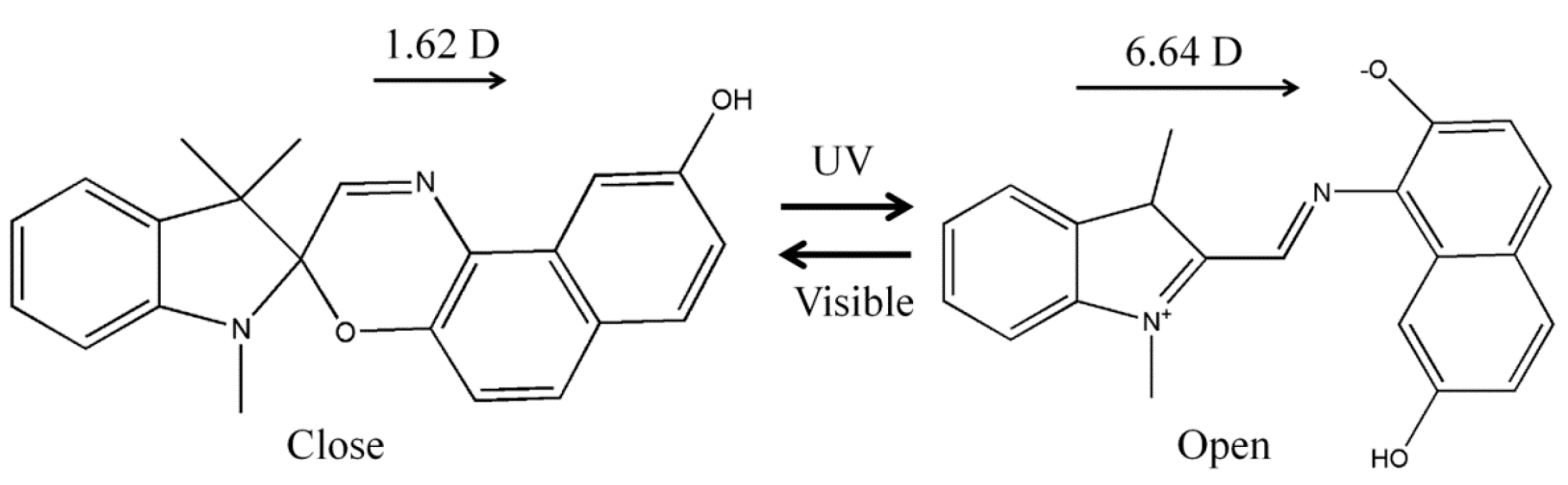
:1. Introduction
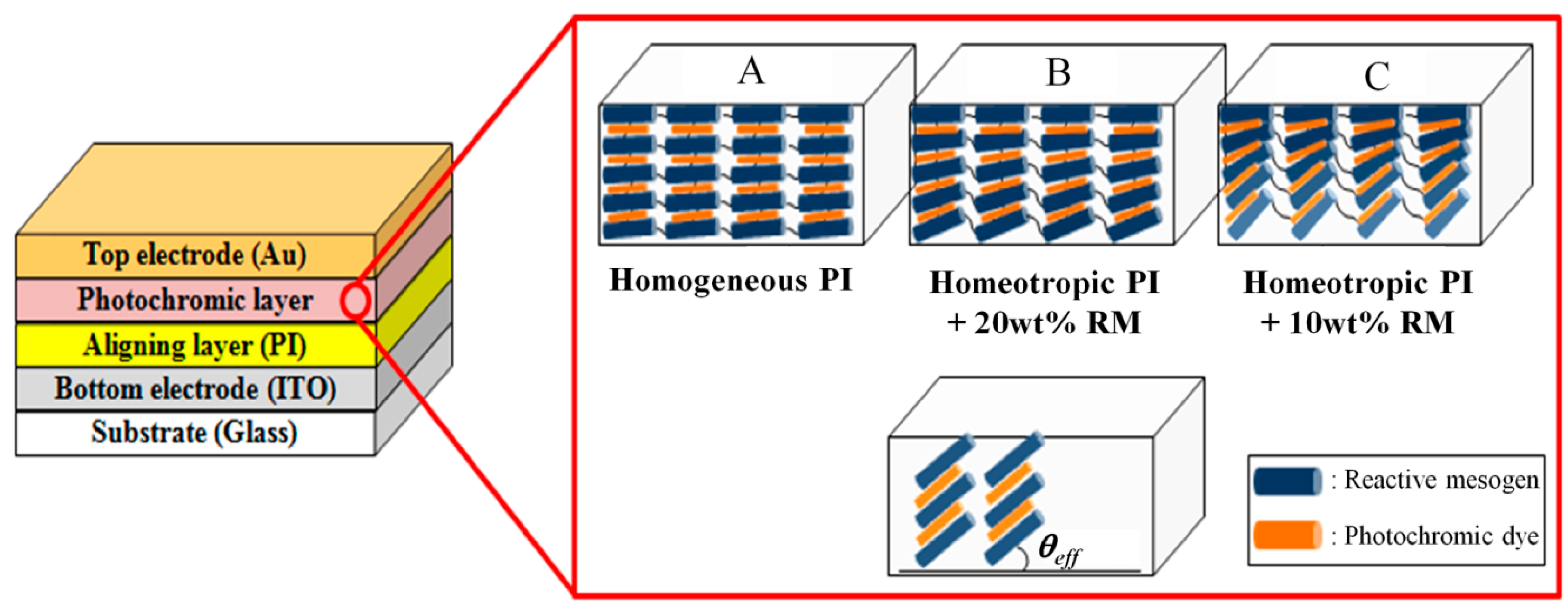
2. Operation Scheme and Experimental Procedure
2.1. Materials and Film Preparation

2.2. Orientation Control with Alignment Layer

2.3. MIM Structure for Electrical Measurement
3. Results and Discussion
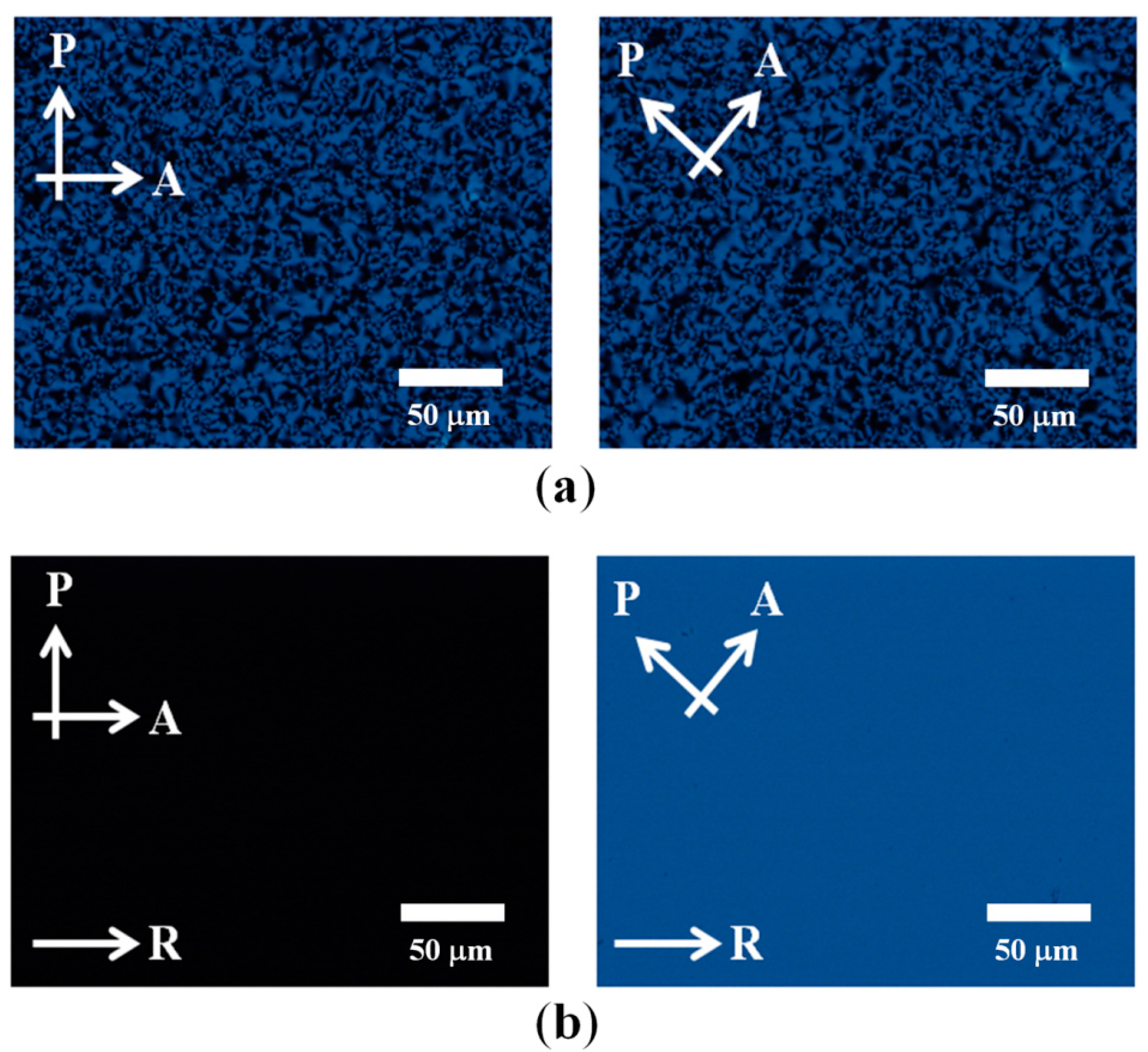
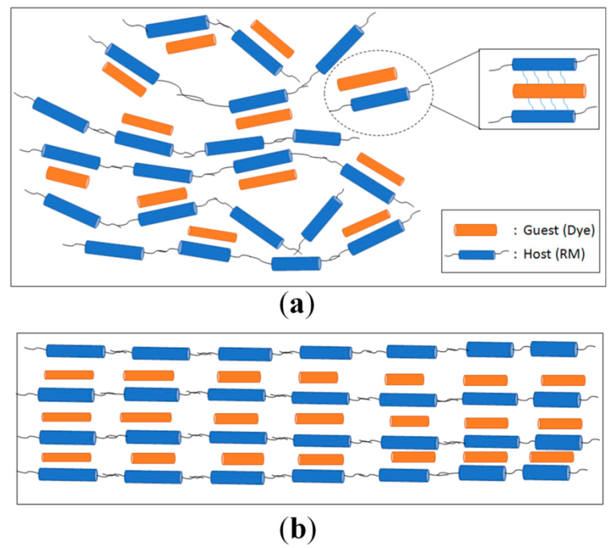
3.1. Control of Photochromic Dye Orientation by Guest-Host Effect


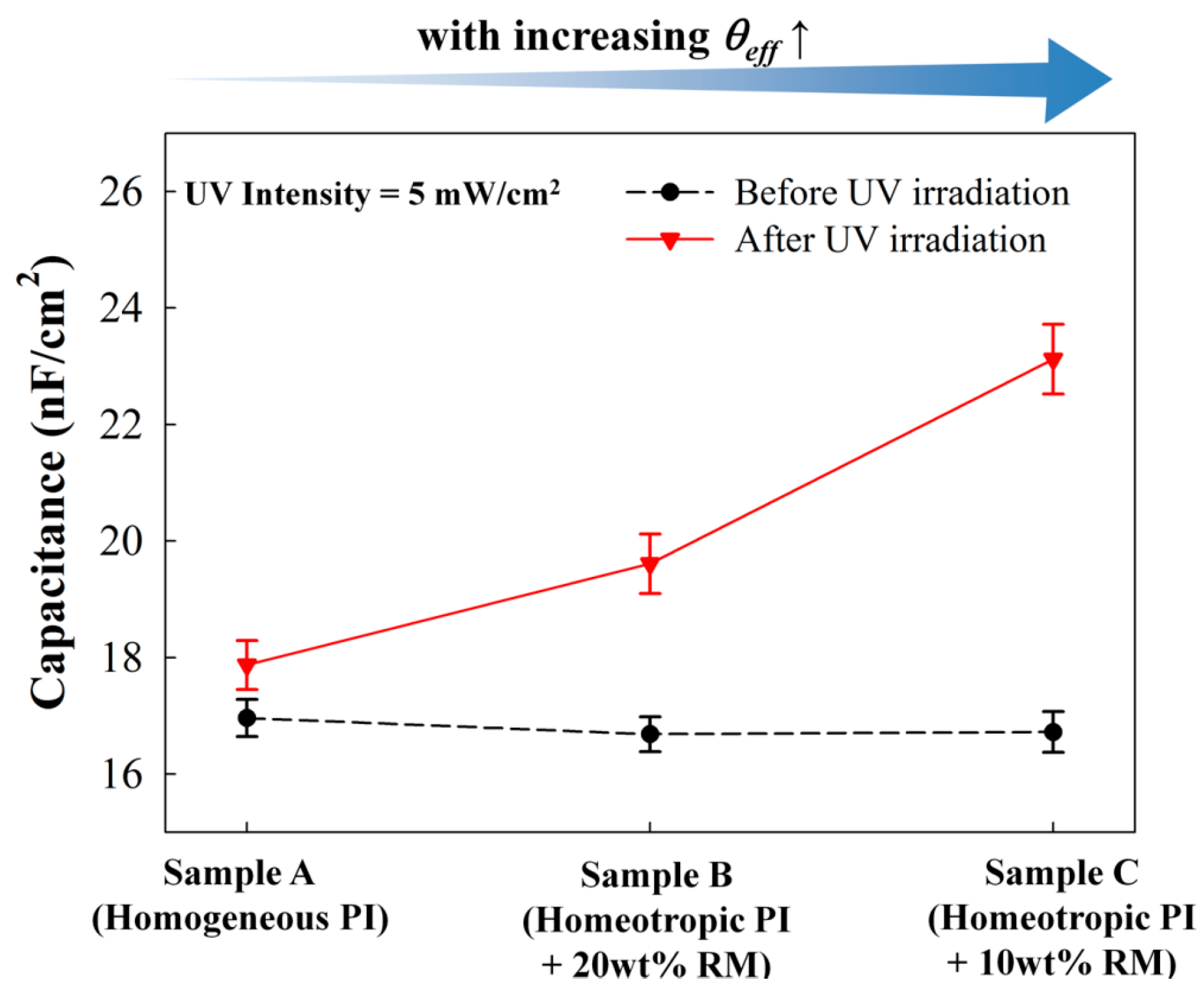
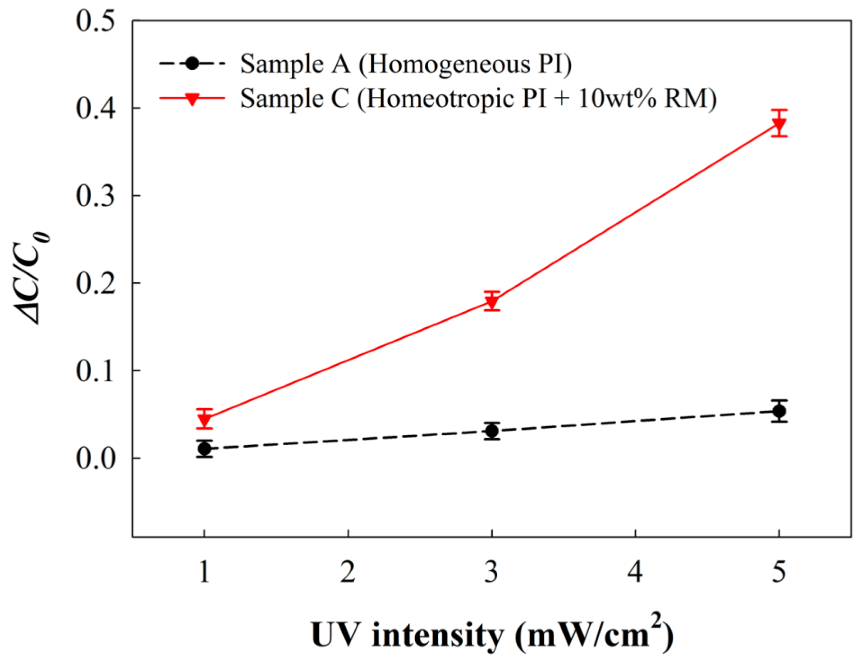
3.2. UV Intensity Sensing by the Capacitance Variation Measurement


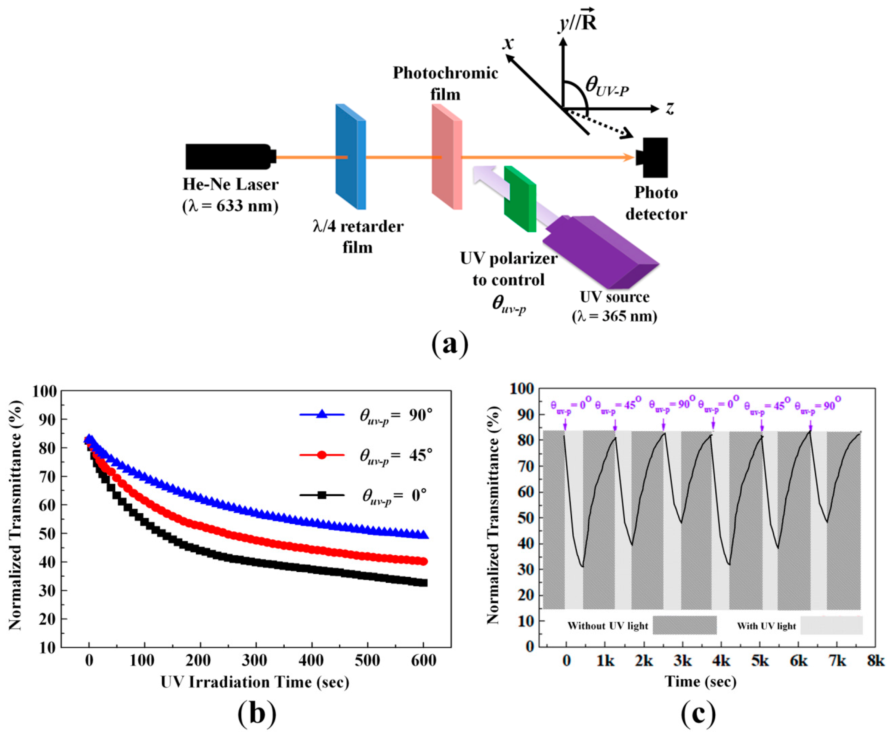
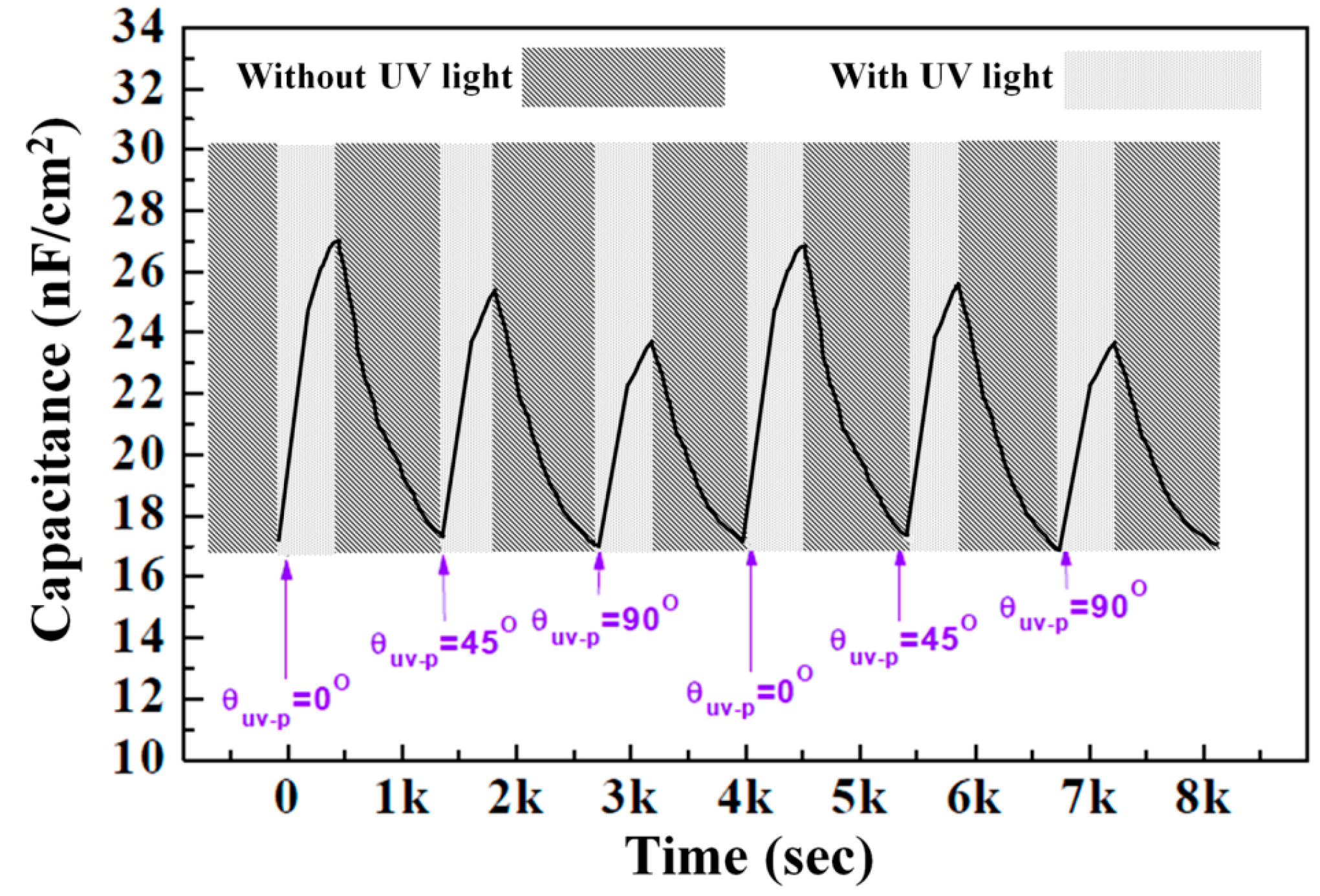
3.3. Polarization-Dependent Capacitance Variation for UV Polarization Measurement


4. Conclusions
Acknowledgments
Author Contributions
Conflicts of Interest
References
- Waynant, R.W.; Ediger, M. Electro-Optics Handbook; McGraw-Hill: New York, NY, USA, 1994; pp. 15.1–15.37. [Google Scholar]
- Phan, D.-T.; Chung, G.-S. Characteristics of SAW UV sensors based on a ZnO/Si structure using third harmonic mode. Curr. Appl. Phys. 2012, 12, 210–213. [Google Scholar] [CrossRef]
- Baltakesmez, A.; Tekmen, S.; Koc, P.; Tuzemen, S.; Meral, K.; Onganer, Y. UV-visible detector and LED based n-ZnO/p-Si heterojunction formed by electrodeposition. AIP Adv. 2013, 3. [Google Scholar] [CrossRef]
- Bayat, K.; Vygranenko, Y.; Sazonov, A.; Baroughi, M.F. Design, fabrication and characterization of an a-Si: H-based UV detector for sunburn applications. Semicond. Sci. Technol. 2006, 21, 1699–1702. [Google Scholar] [CrossRef]
- Tu, M.-L.; Su, Y.-K.; Chang, S.-J.; Chuang, R.W. GaN UV photodetector by using transparency antimony doped tin oxide electrode. J. Cryst. Growth 2007, 298, 744–747. [Google Scholar] [CrossRef]
- Lin, C.R.; Wei, D.H.; BenDao, M.K.; Chen, W.E.; Liu, T.Y. Development of high performance UV detector using nanocrystalline diamond thin film. Int. J. Photoenergy 2014, 2014. [Google Scholar] [CrossRef]
- Amin, M.; Manzoor, U.; Islam, M.; Bhatti, A.S.; Shah, N.A. Synthesis of ZnO nanostructures for low temperature CO and UV sensing. Sensors 2012, 12, 13842–13851. [Google Scholar] [CrossRef] [PubMed]
- Palais, J.C. Fiber Optic Communications, 4th ed.; Prentice-Hall: Englewood Cliffs, NJ, USA, 1998; pp. 87–93. [Google Scholar]
- Kim, S.-H.; Suh, H.-J.; Cui, J.-Z.; Gal, Y.-S.; Jin, S.-H.; Koh, K. Crystalline-state photochromism and thermochromism of new spiroxazine. Dyes Pigment. 2002, 53, 251–256. [Google Scholar] [CrossRef]
- Irie, M.; Fukaminato, T.; Matsuda, K.; Kobatake, S. Photochromism of diarylethene molecules and crystals: Memories, switches, and actuators. Chem. Rev. 2014, 114, 12174–12277. [Google Scholar] [CrossRef] [PubMed]
- Kawata, S.; Kawata, Y. Three dimensional optical data storage using photochromic materials. Chem. Rev. 2000, 100, 1777–1788. [Google Scholar] [CrossRef] [PubMed]
- Péreza, G.B.; Huertaa, F.L.; Aguirrea, S.M.; Mixcóatla, J.C.; Merinoa, R.P.; Morales, R.L.; Moreno, O.P. Fabrication and characterization of an optical fiber pH sensor using sol–gel deposited TiO2 film doped with organic dyes. Sens. Actuators B Chem. 2006, 120, 74–78. [Google Scholar] [CrossRef]
- Zhu, M.-Q.; Zhu, L.; Han, J.J.; Wu, W.; Hurst, J.K.; Li, A.D.Q. Spiropyran-based photochromic polymer nanoparticles with optically switchable luminescence. J. Am. Chem. Soc. 2006, 128, 4303–4309. [Google Scholar] [CrossRef] [PubMed]
- Ready, J. Fundamentals of photonics. In Optical Detectors and Human Vision; SPIE: Saint Paul, MN, USA, 1999; pp. 211–248. [Google Scholar]
- Ock, K.; Jo, N.; Kim, J.; Kim, S.; Koh, K. Thin film optical waveguide type UV sensor using a photochromic molecular device, spirooxazine. Synth. Met. 2001, 117, 131–133. [Google Scholar] [CrossRef]
- Shen, Q.; Wang, L.; Liu, S.; Cao, Y.; Gan, L.; Guo, X.; Steigerwald, M.L.; Shuai, Z.; Liu, Z.; Nuckolls, C. Photoactive gate dielectrics. Adv. Mater. 2010, 22, 3282–3287. [Google Scholar] [CrossRef] [PubMed]
- Zhang, H.; Guo, X.; Hui, J.; Hu, S.; Xu, W.; Zhu, D. Interface engineering of semiconductor/dielectric heterojunctions toward functional organic thin film transistor. Nano Lett. 2011, 11, 4939–4946. [Google Scholar] [CrossRef] [PubMed]
- Xie, X.; Mistlberger, G.; Bakker, E. Reversible photodynamic chloride-selective sensor based on photochromic spiropyran. J. Am. Chem. Soc. 2012, 134, 16929–16932. [Google Scholar] [CrossRef] [PubMed]
- Guo, X.; Huang, L.; O’Brien, S.; Kim, P.; Nuckolls, C. Directing and sensing changes in molecular conformation on individual carbon nanotube field effect transistors. J. Am. Chem. Soc. 2005, 127, 15045–15047. [Google Scholar] [CrossRef] [PubMed]
- Shao, N.; Zhang, Y.; Cheung, S.; Yang, R.; Chan, W.; Mo, T.; Li, K.; Liu, F. Copper ion-selective fluorescent sensor based on the inner filter effect using a spiropyran derivative. Anal. Chem. 2005, 77, 7294–7303. [Google Scholar] [CrossRef] [PubMed]
- Zhu, S.; Li, M.; Sheng, L.; Chen, P.; Zhang, Y.; Zhang, S.X.-A. A spirooxazine derivative as a highly sensitive cyanide sensor by means of UV-visible difference spectroscopy. Analyst 2012, 137, 5581–5585. [Google Scholar] [CrossRef] [PubMed]
- Jang, S.-W.; Son, S.-J.; Kim, D.-E.; Kwon, D.-H.; Kim, S.-H.; Lee, Y.-H.; Kang, S.-W. UV-sensitive photo functional device using evanescent field absorption between SU-8 polymer optical waveguide and photochromic dye. IEEE Photonics Technol. Lett. 2006, 18, 82–84. [Google Scholar] [CrossRef]
- Berkovic, G.; Krongauz, V.; Weiss, V. Spiropyrans and spirooxazines for memories and switches. Chem. Rev. 2000, 100, 1741–1753. [Google Scholar] [CrossRef] [PubMed]
- Tomasulo, M.; Sortino, S.; White, A.J.P.; Raymo, F.M. Fast and stable photochromic oxazines. J. Org. Chem. 2005, 70, 8180–8189. [Google Scholar] [CrossRef] [PubMed]
- Tomasulo, M.; Sortino, S.; Raymo, F.M. A fast and stable photochromic switch based on the opening and closing of an oxazine ring. Org. Lett. 2005, 7, 1109–1112. [Google Scholar] [CrossRef] [PubMed]
- Ku, C.-J.; Reyes, P.; Duan, Z.; Hong, W.-C.; Li, R.; Lu, Y. Mgx Zn1−xO Thin film transistor-based UV photodetector with enhanced photoresponse. J. Electron. Mater. 2015, 44, 3471–3476. [Google Scholar] [CrossRef]
- Chang, S.; Ju, B.-K.; Yakuphanoglu, F. Ultraviolet and visible light detection characteristics of amorphous indium gallium zinc oxide thin film transistor for photodetector applications. Int. J. Adv. Smart Converg. 2012, 1, 61–64. [Google Scholar] [CrossRef]
- Lee, K.W.; Heo, K.Y.; Kim, H.J. Photosensitivity of solution-based indium gallium zinc oxide single-walled carbon nanotubes blend thin film transistors. Appl. Phys. Lett. 2009, 94. [Google Scholar] [CrossRef]
- Wang, W.J.; Shan, C.X.; Zhu, H.; Ma, F.Y.; Shen, D.Z.; Fan, X.W.; Choy, K.L. Metal-insulator-semiconductor-insulator-metal structured titanium dioxide ultraviolet photodetector. J. Phys. D Appl. Phys. 2010, 43. [Google Scholar] [CrossRef]
- Lee, C.-J.; Kwon, Y.-J.; Won, C.-H.; Lee, J.-H.; Hahm, S.-H. Dual-wavelength sensitive AlGaN/GaN metal-insulator-semiconductor-insulator-metal ultraviolet sensor with balanced ultraviolet/visible rejection ratios. Appl. Phys. Lett. 2013, 103. [Google Scholar] [CrossRef]
- Xue, H.; Kong, X.; Liu, Z.; Liu, C.; Zhou, J.; Chen, W.; Ruan, S.; Xu, Q. TiO2 based metal-semiconductor-metal ultraviolet photodetectors. Appl. Phys. Lett. 2007, 90. [Google Scholar] [CrossRef]
- Selman, A.M.; Hassan, Z. Effects of variations in precursor concentration on the growth of rutile TiO2 nanorods on Si substrate with fabricated fast-response metal-semiconductor-metal UV detector. Opt. Mater. 2015, 44, 37–47. [Google Scholar] [CrossRef]
- Chen, G.Y.; Wang, Z. Towards extremely sensitive ultraviolet-light sensors employing photochromic optical microfiber. J. Sens. 2015, 2015. [Google Scholar] [CrossRef]
- Oh, S.-W.; Lee, D.-J.; Park, M.-K.; Park, K.H.; Lee, J.-H.; Kim, B.K.; Kim, H.-R. Enhancement of viewing angle properties of a single-domain fringe-field switching mode using zero pretilt alignment. J. Phys. D Appl. Phys. 2015, 48. [Google Scholar] [CrossRef]
- Yaroschchuk, O.; Kyrychenko, V.; Tao, D.; Chigrinov, V.; Kwok, H.S.; Hasebe, H.; Takatsu, H. Stabilization of liquid crystal photo aligning layers by reactive mesogens. Appl. Phys. Lett. 2009, 95. [Google Scholar] [CrossRef]
- Ishinabe, T.; Miyashita, T.; Uchida, T. Novel wide viewing angle polarizer with high achromaticity. SID Int. Symp. Dig. Tech. 2000, 31, 1094–1097. [Google Scholar] [CrossRef]
- Chung, H.-K.; Lee, W.-K.; Park, H.-G.; Lee, H.M.; Jeong, H.-C.; Cho, M.-C.; Seo, D.-S. Polarized UV cured reactive mesogens for fast switching and low voltage driving liquid crystal device. Opt. Express 2014, 22, 21551–21559. [Google Scholar] [CrossRef] [PubMed]
- Lee, Y.-J.; Baek, J.-H.; Kim, Y.; Heo, J.U.; Yu, C.-J.; Kim, J.-H. Enhanced surface anchoring energy for the photo-alignment layer with reactive mesogens for fast response time of liquid crystal displays. J. Phys. D Appl. Phys. 2013, 46. [Google Scholar] [CrossRef]
- Seo, D.S.; Araya, K.; Yoshida, N.; Nishikawa, M.; Yabe, Y.; Kobayashi, S. Effect of the polymer tilt angle for generation of pretilt angle in nematic liquid crystal on rubbed polyimide surfaces. Jpn. J. Appl. Phys. 1995, 34. [Google Scholar] [CrossRef]
- Kim, K.H.; Baek, J.I.; Cheong, B.H.; Choi, H.Y.; Shin, S.T.; Kim, J.C.; Yoon, T.H. Pretilt angle control and multidomain alignment of liquid crystals by using polyimide mixed with liquid crystalline prepolymer. Appl. Phys. Lett. 2010, 96. [Google Scholar] [CrossRef]
- Kamiya, T.; Saito, F.; Wada, O.; Yajima, H. Femtosecond Technology from Basic Research to Application Prospects; Springer Series in Photonics: Heidelberg, Germany, 1999; pp. 390–397. [Google Scholar]
- Klajn, R. Spiropyran-based dynamic materials. Chem. Soc. Rev. 2014, 43, 148–184. [Google Scholar] [CrossRef] [PubMed]
- Hanemann, T.; Haase, W. Orientational behavior of Stilbene dyes in nematic liquid crystals. Mol. Cryst. Liq. Cryst. 1993, 231, 119–127. [Google Scholar] [CrossRef]
- Schmidt, H.W. Dichroic dyes and liquid crystalline side chain polymers. Angew. Chem. Int. Ed. 1989, 101, 964–970. [Google Scholar] [CrossRef]
- Peeters, E.; Lub, J.; Steenbakkers, J.A.M.; Broer, D.J. High-contrast thin film polarizers by photo-crosslinking of smectic Guest-Host systems. Adv. Mater. 2006, 18, 2412–2417. [Google Scholar] [CrossRef]
- Zhao, X.; Boussaid, F.; Bermak, A.; Chigrinov, V.G. High-resolution thin “guest-host” micropolarizer arrays for visible imaging polarimetry. Opt. Express 2011, 19, 5565–5573. [Google Scholar] [CrossRef] [PubMed]
- Yaroshchuk, O.; Reznikov, Y. Photoalignment of liquid crystals: Basics and current trends. J. Mater. Chem. 2012, 22, 286–300. [Google Scholar] [CrossRef]
- Lee, Y.-J.; Kim, Y.-K.; Jo, S.I.; Gwag, J.S.; Yu, C.-J.; Kim, J.-H. Surface-controlled patterned vertical alignment mode with reactive mesogen. Opt. Express. 2009, 17, 10298–10303. [Google Scholar] [CrossRef] [PubMed]
- Lee, Y.-J.; Yu, C.-J.; Kim, Y.-K.; Jo, S.I.; Kim, J.-H. Direct image of a molecular orientation of a liquid crystal using directional polymerization of photo reactive mesogen. Appl. Phys. Lett. 2011, 98. [Google Scholar] [CrossRef]
- Park, H.-G.; Lee, H.M.; Jeong, H.-C.; Seo, D.-S. Fast switching of liquid crystals on transferred reactive mesogens film via soft imprinting method. RSC Adv. 2014, 4, 34610–34614. [Google Scholar] [CrossRef]
- Moon, Y.-K.; Kim, T.-M.; Choi, M.-G.; Jeong, J.-H.; Lee, Y.-J.; Yu, C.-J.; Kim, Y.M.; Kim, J.-H. Control of liquid crystal pre-tilt angle using reactive mesogen. SID Int. Symp. Dig. Tech. 2011, 42, 1630–1632. [Google Scholar] [CrossRef]
- Kim, S.M.; Cho, I.Y.; Kim, W.I.; Jeong, K.-U.; Lee, S.H.; Lee, G.D.; Son, J.; Lyu, J.-J.; Kim, K.H. Surface-Modification on Vertical Alignment Layer Using UV-Curable Reactive Mesogens. Jpn. J. Appl. Phys. 2009, 48. [Google Scholar] [CrossRef]
- Moon, Y.-K.; Lee, Y.-J.; Jo, S.I.; Kim, Y.; Heo, J.U.; Baek, J.-H.; Kang, S.-G.; Yu, C.-J.; Kim, J.-H. Effects of surface modification with reactive mesogen on the anchoring strength of liquid crystals. J. Appl. Phys. 2013, 113. [Google Scholar] [CrossRef]
- Lin, J.-S. Interaction between dispersed photochromic compound and polymer matrix. Eur. Polym. J. 2003, 39, 1693–1700. [Google Scholar] [CrossRef]
- Li, Y.; Zhang, H.; Qi, C.; Guo, X. Light-driven photochromism-induced reversible switching in P3HT-spiropyran hybrid transistors. J. Mater. Chem. 2012, 22, 4261–4265. [Google Scholar] [CrossRef]
- Aghamohammadi, M.; Rödel, R.; Zschieschang, U.; Ocal, C.; Boschker, H.; Weitz, R.T.; Barrena, E.; Klauk, H. Threshold-voltage shifts in organic transistors due to self-assembled monolayers at the dielectric: Evidence for electronic coupling and dipolar effects. ACS Appl. Mater. Interfaces 2015, 7, 22775–22785. [Google Scholar] [CrossRef] [PubMed]
© 2015 by the authors; licensee MDPI, Basel, Switzerland. This article is an open access article distributed under the terms and conditions of the Creative Commons by Attribution (CC-BY) license (http://creativecommons.org/licenses/by/4.0/).
Share and Cite
Ranjkesh, A.; Park, M.-K.; Park, D.H.; Park, J.-S.; Choi, J.-C.; Kim, S.-H.; Kim, H.-R. Tilted Orientation of Photochromic Dyes with Guest-Host Effect of Liquid Crystalline Polymer Matrix for Electrical UV Sensing. Sensors 2016, 16, 38. https://doi.org/10.3390/s16010038
Ranjkesh A, Park M-K, Park DH, Park J-S, Choi J-C, Kim S-H, Kim H-R. Tilted Orientation of Photochromic Dyes with Guest-Host Effect of Liquid Crystalline Polymer Matrix for Electrical UV Sensing. Sensors. 2016; 16(1):38. https://doi.org/10.3390/s16010038
Chicago/Turabian StyleRanjkesh, Amid, Min-Kyu Park, Do Hyuk Park, Ji-Sub Park, Jun-Chan Choi, Sung-Hoon Kim, and Hak-Rin Kim. 2016. "Tilted Orientation of Photochromic Dyes with Guest-Host Effect of Liquid Crystalline Polymer Matrix for Electrical UV Sensing" Sensors 16, no. 1: 38. https://doi.org/10.3390/s16010038