A First Step Towards a Microfabricated Thin-Film Sensor Array on the Basis of Chalcogenide Glass Materials

Abstract
:Introduction
Experimental
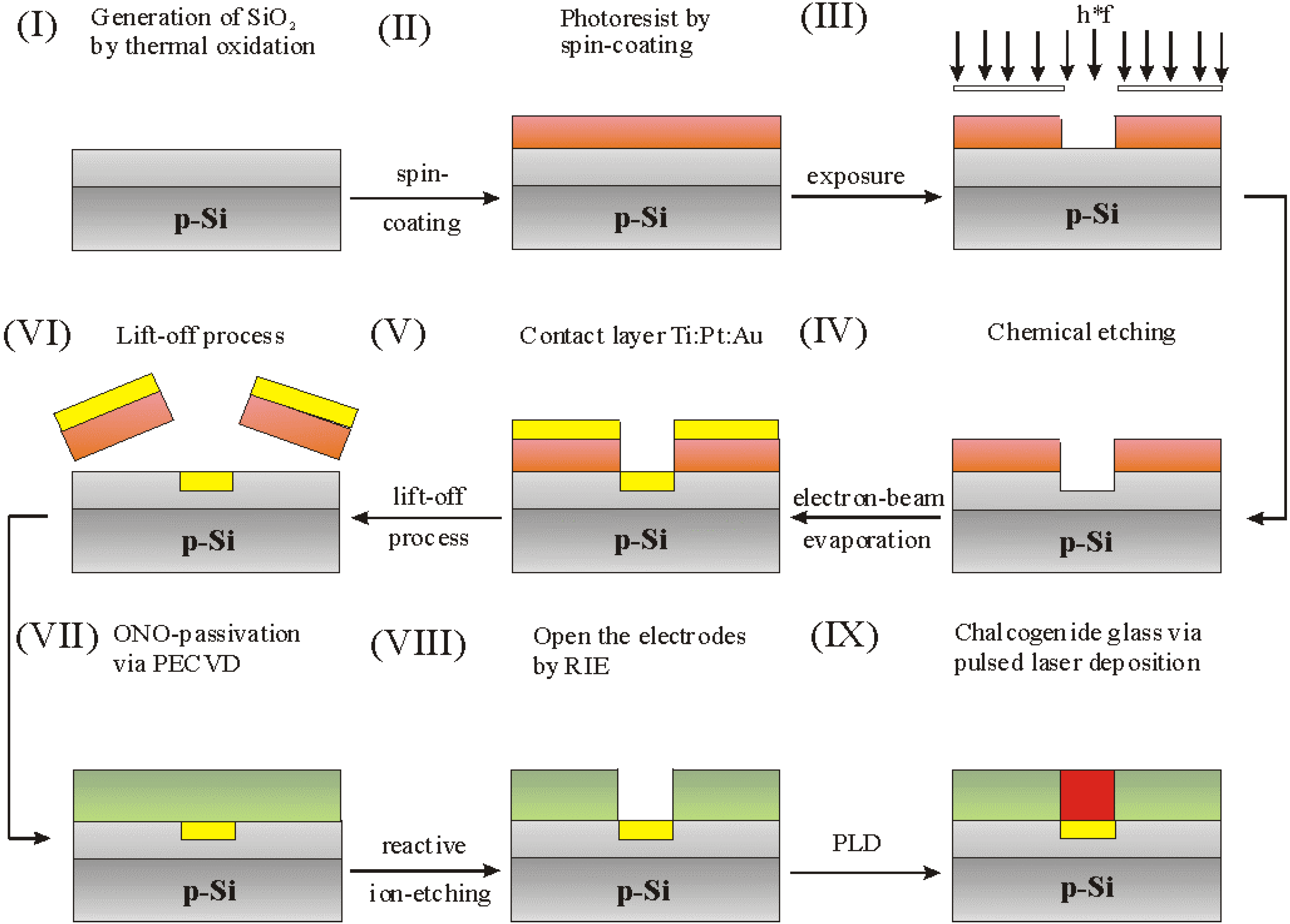
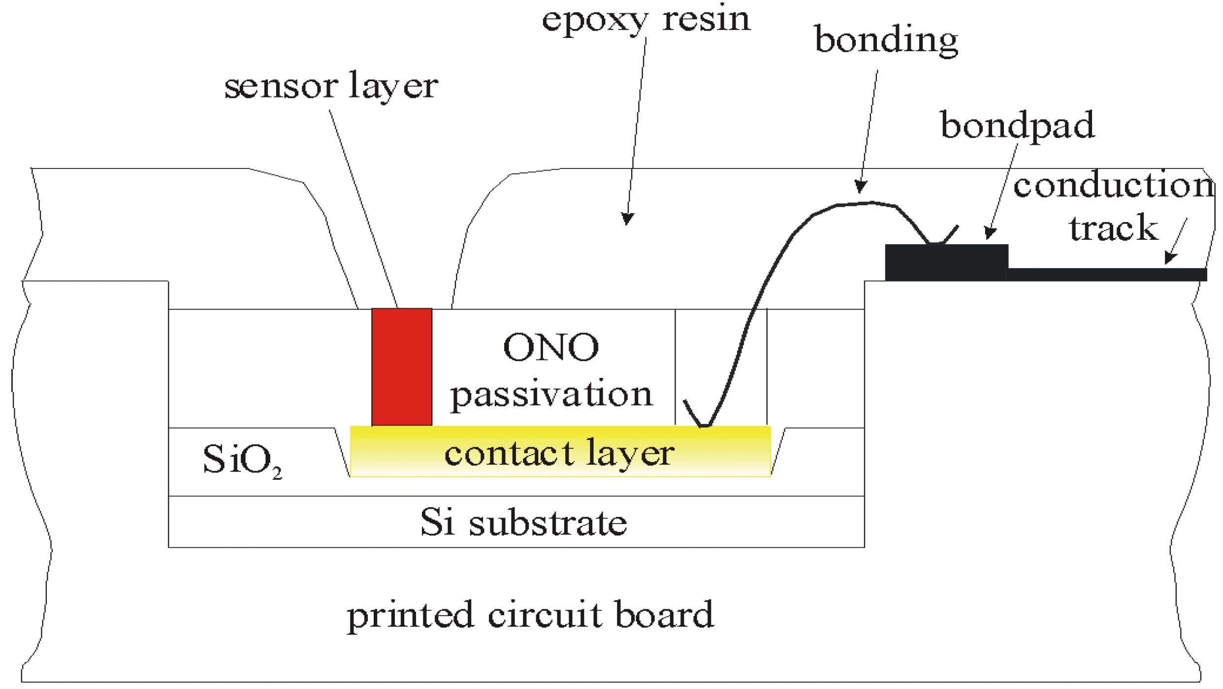
Fabrication of the Chalcogenide Glass-Based Thin-Film Sensor Array


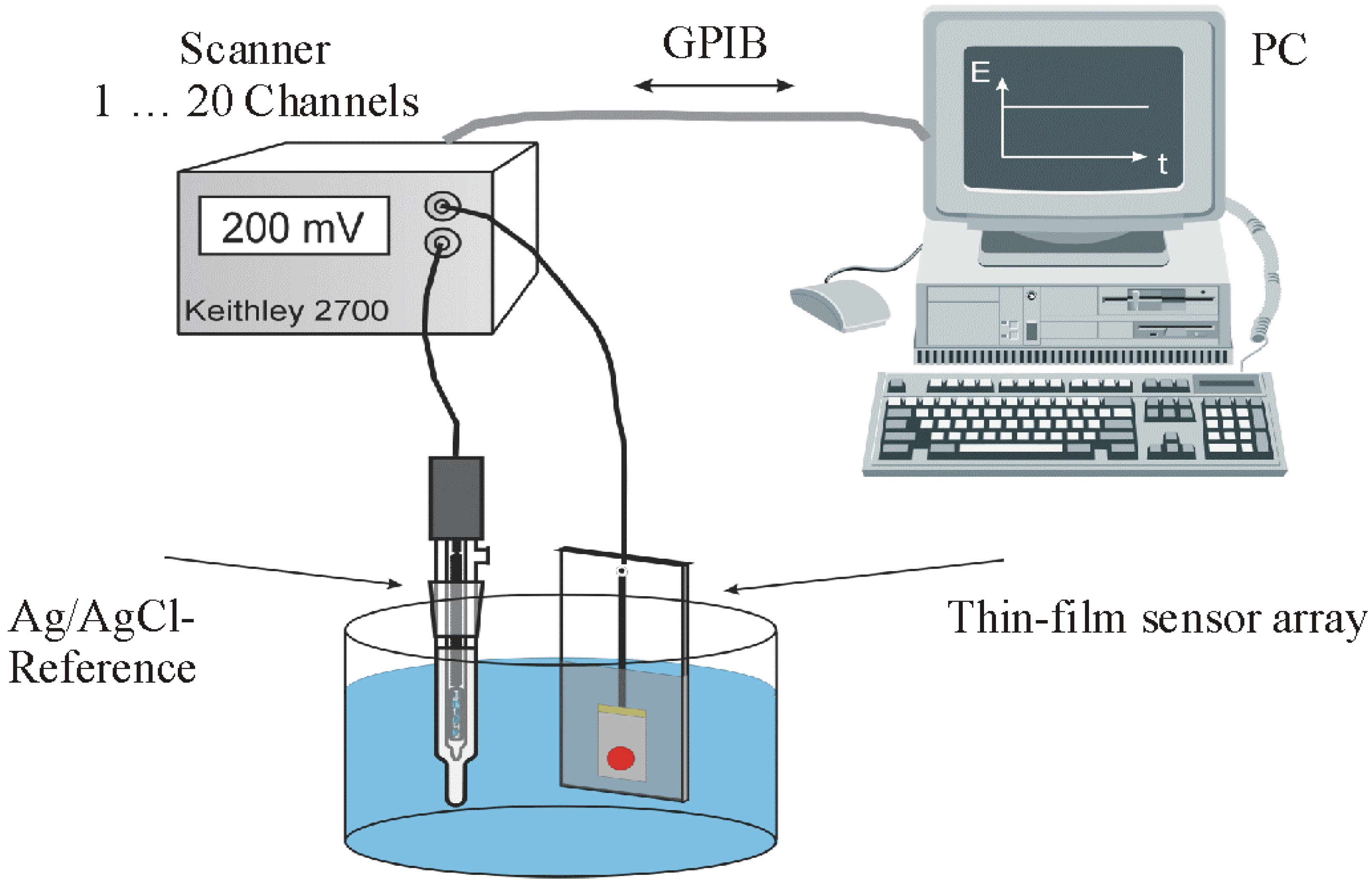
Physical and Electrochemical Characterization of the Chalcogenide Glass-Based Thin-Film Sensor Array

Results and Discussion
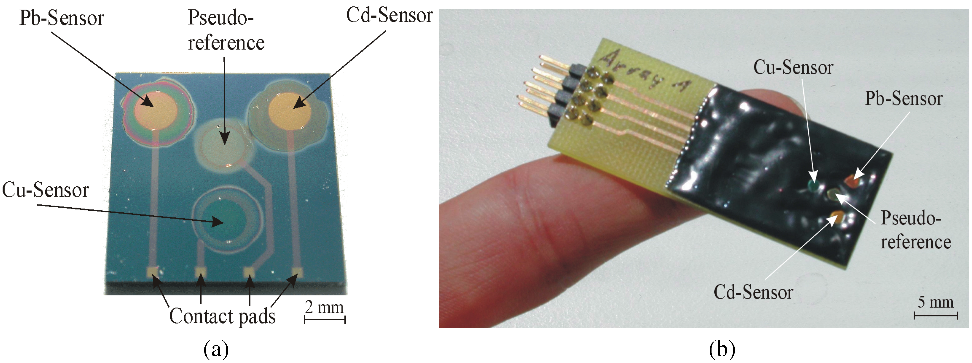
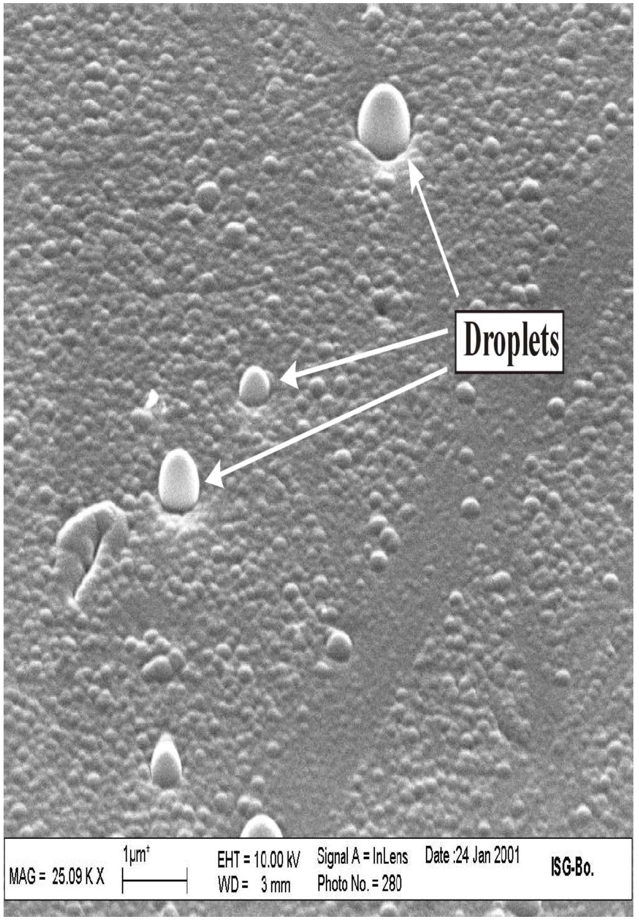
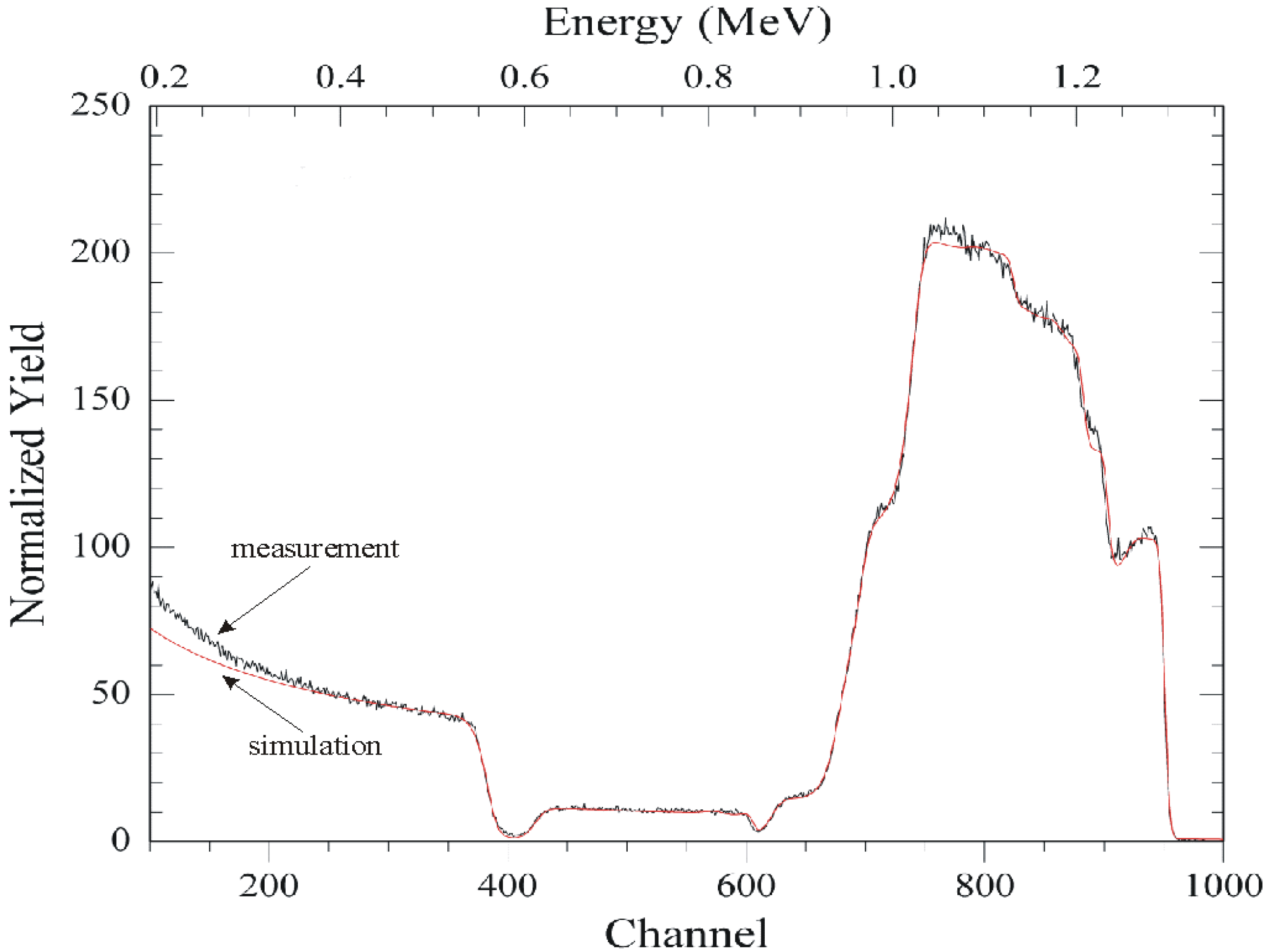
Physical Characterization of the Chalcogenide Glass-Based Thin-Film Sensor Array


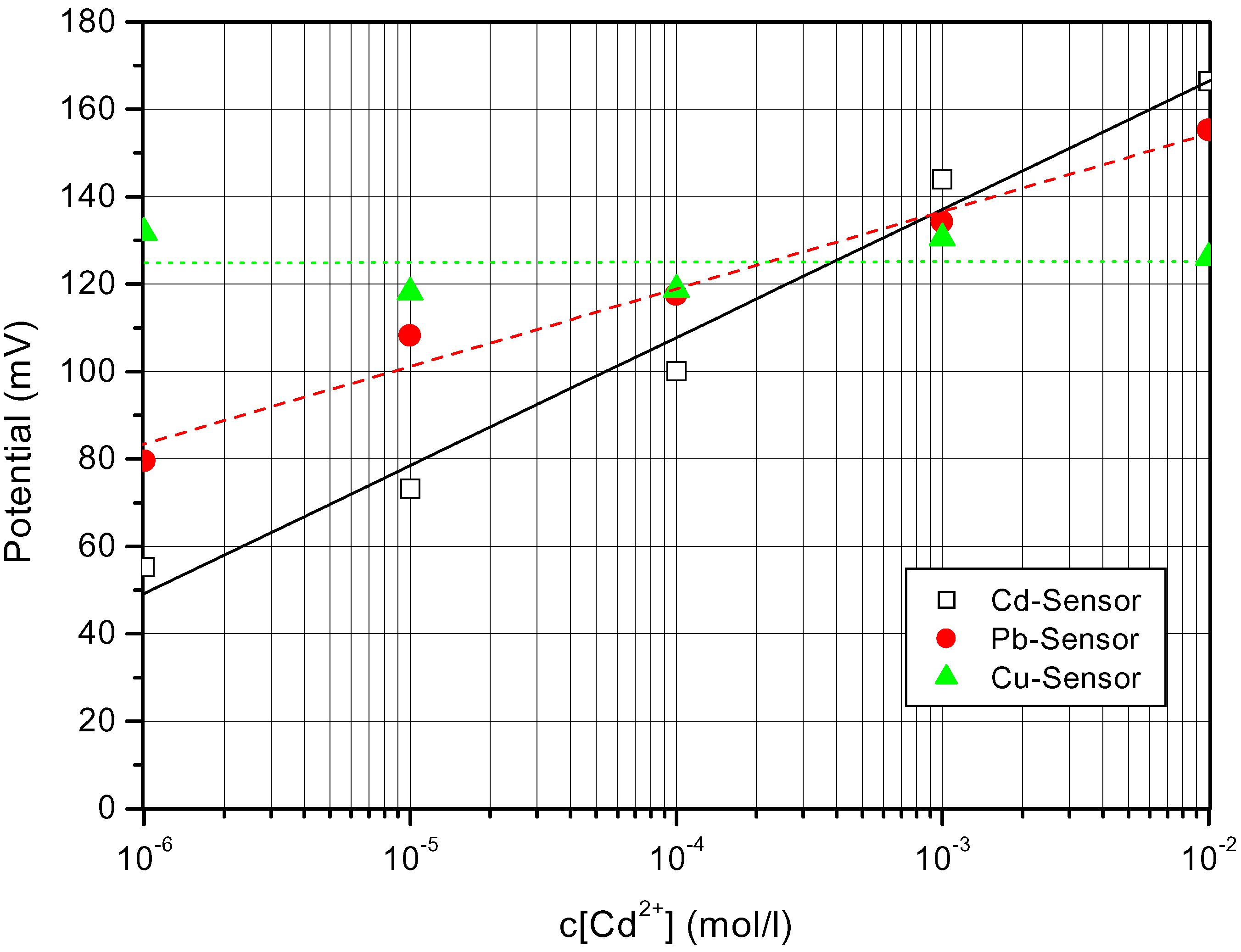
Electrochemical Characterization of the Chalcogenide Glass-Based Thin-Film Sensor Array

Conclusions and Perspectives
Acknowledgements
References
- Ahlers, H. Multisensorikpraxis; Springer-Verlag: Berlin, Heidelberg; New York, 1996; pp. 182–365. [Google Scholar]
- Henze, G.; Köhler, M.; Lay, J.P. Umweltdiagnostik mit Mikrosystemen; Wiley-VCH: Weinheim, 1999; pp. 1–62. [Google Scholar]
- D’Amico, A.; Di Natale, C.; Paolesse, R. Portraits of gasses and liquids by arrays of nonspecific chemical sensors: trends and perspectives. Sens. Act. B 2000, 68, 324–330. [Google Scholar] [CrossRef]
- Mourzina, Yu. G.; Schubert, J.; Zander, W.; Legin, A.; Vlasov, Yu. G.; Lüth, H.; Schöning, M.J. Development of multisensor systems based on chalcogenide thin film chemical sensors for the simultaneous multicomponent analysis of metal ions in complex solutions. Electrochim. Act. 2001, 47, 251–258. [Google Scholar] [CrossRef]
- Vlasov, Yu.G.; Legin, A.V. Non-selective chemical sensors in analytical chemistry: from “electronic nose” to “electronic tongue”. Fresenius J. Anal. Chem. 1998, 361, 255–260. [Google Scholar] [CrossRef]
- Vlasov, Yu.; Legin, A.; Rudnitskaya, A. Electronic tongues and their analytical application. Anal. Bioanal. Chem. 2002, 373, 136–146. [Google Scholar] [CrossRef] [PubMed]
- Vlasov, Yu.G.; Bychkov, E.A. Ion-selective chalcogenide glass electrodes. Ion- selective Electrode Rev. 1987, 9, 5–93. [Google Scholar]
- Vlasov, Yu.G.; Legin, A.; Rudnitskaya, A. Cross-sensitivity evaluation of chemical sensors for electronic tongue: determination of heavy metal ions. Sens. Act. B 1997, 44, 532–537. [Google Scholar] [CrossRef]
- Schöning, M.J.; Mourzina, Yu.G.; Schubert, J.; Zander, W.; Legin, A.; Vlasov, Yu.G.; Lüth, H. Pulsed laser deposition – an innovative technique for preparing inorganic thin films. Electroanal. 2001, 13(8–9), 727–732. [Google Scholar] [CrossRef]
- Schöning, M.J.; Mourzina, Yu.G.; Schubert, J.; Zander, W.; Legin, A.; Vlasov, Yu.G.; Lüth, H. Can pulsed laser deposition serve as an advanced technique in fabricating chemical sensors ? Sens. Act. B 2001, 78, 273–278. [Google Scholar] [CrossRef]
- Vlasov, Yu.G. New solid-state ion-selective electrodes – sensors for chemical analysis of solutions. Fresenius Z. Anal. Chem. 1989, 355, 92–99. [Google Scholar] [CrossRef]
- Fassbender, F.; Schmitt, G.; Schöning, M.J.; Lüth, H.; Buß, G.; Schultze, J.-W. Optimization of passivation layers for corrosion protection of silicon-based microelectrode arrays. Sens. Act. B 2000, 68, 128–133. [Google Scholar] [CrossRef]
- Schöning, M.J.; Schmidt, C.; Schubert, J.; Zander, W.; Mesters, S.; Kordos, P.; Lüth, H.; Legin, A.; Seleznev, B.; Vlasov, Yu.G. Thin film sensors on the basis of chalcogenide glass materials prepared by pulsed laser deposition technique. Sens. Act. B 2000, 68, 254–259. [Google Scholar] [CrossRef]
- Mourzina, Yu.G.; Schöning, M.J.; Schubert, J.; Zander, W.; Legin, A.; Vlasov, Yu.G.; Kordos, P.; Lüth, H. A new thin-film Pb microsensor based on chalcogenide glasses. Sens. Act. B 2000, 71, 13–18. [Google Scholar] [CrossRef]
- Sample Availability: Available from the authors.
© 2002 by MDPI (http://www.mdpi.net). Reproduction is permitted for noncommercial purposes.
Share and Cite
Kloock, J.P.; Mourzina, Y.G.; Schubert, J.; Schöning, M.J. A First Step Towards a Microfabricated Thin-Film Sensor Array on the Basis of Chalcogenide Glass Materials. Sensors 2002, 2, 356-365. https://doi.org/10.3390/s20900356
Kloock JP, Mourzina YG, Schubert J, Schöning MJ. A First Step Towards a Microfabricated Thin-Film Sensor Array on the Basis of Chalcogenide Glass Materials. Sensors. 2002; 2(9):356-365. https://doi.org/10.3390/s20900356
Chicago/Turabian StyleKloock, Joachim P., Yulia G. Mourzina, Jürgen Schubert, and Michael J. Schöning. 2002. "A First Step Towards a Microfabricated Thin-Film Sensor Array on the Basis of Chalcogenide Glass Materials" Sensors 2, no. 9: 356-365. https://doi.org/10.3390/s20900356