A Concept for a Sensitive Micro Total Analysis System for High Throughput Fluorescence Imaging

1
Tel-Aviv University, Physical Electronics Department, Ramat-Aviv, Tel-Aviv 69978, Israel
2
School of Applied Chemistry, Waseda University, Step 21, #40 31-103 Titsuka-cho, Shinjuku-ku, Tokyo, Japan
*
Author to whom correspondence should be addressed.
Sensors 2006, 6(4), 341-349; https://doi.org/10.3390/S6040341
Submission received: 26 June 2005
/
Accepted: 4 January 2006
/
Published: 7 April 2006
Abstract
:This paper discusses possible methods for on-chip fluorescent imaging for integrated bio-sensors. The integration of optical and electro-optical accessories, according to suggested methods, can improve the performance of fluorescence imaging. It can boost the signal to background ratio by a few orders of magnitudes in comparison to conventional discrete setups. The methods that are present in this paper are oriented towards building reproducible arrays for high-throughput micro total analysis systems (μTAS). The first method relates to side illumination of the fluorescent material placed into micro-compartments of the lab-on-chip. Its significance is in high utilization of excitation energy for low concentration of fluorescent material. The utilization of a transparent μLED chip, for the second method, allows the placement of the excitation light sources on the same optical axis with emission detector, such that the excitation and emission rays are directed controversly. The third method presents a spatial filtering of the excitation background.
Keywords:
Fluorescence; imaging; lab-on-chip; μfluidic; lenslet array; μLED chip; image sensor; biosensorIntroduction
A variety of bio-sensing schemes have been developed for biotechnology applications such as genomics, health diagnostics, in vivo/vitro sensing, chemical and biological hazards detection, environmental control, etc. One of those applications is the fluorescence detection which is offering several advantages such as sensitivity and specificity. Currently, a fluorescence-based instrumentation is complicated, expensive and not compact enough to be used in field-deployable applications that are becoming more and more desired on consumer and military markets. Therefore, the research and development of integrated, low cost, compact, high-throughput and sensitive bio-fluorescence integrated systems is very important.
Any fluorescence-based technology requires an excitation light source, emission detector and additional optical components such as optical filters, waveguides, mirrors, etc. Optical filters are required to prevent the excitation light rays reaching the emission detector. Unfiltered excitation rays are creating an “excitation background” that can be the limiting factor that determines the sensitivity of the fluorescence-based detection system.
A simple method to significantly decease the excitation background is by positioning a directed excitation light source off-axis, i.e. it is on an axis not intersecting with the emission detector. Evidently, there are two such possible configurations: (i) the excitation rays are perpendicular to emission rays; and (ii) both excitation and emission rays are on the same optical axis directed controversially. However, the implementation of those configurations in a miniature high-throughput integrated system is challenging as it requires a complicated optical paths design and special alignment requirements that affect the system size, complexity and cost.
The monolithic integration of vertical cavity surface emitting lasers (VCSELs) with PIN photodetectors is a very promising method for fluorescence-based imaging [1,2]. It allows the miniaturization and dramatic increases of simultaneous bio-chemical reactions monitoring. However, this method is limited to Infra-Red (IR) and near IR spectra due to the physical properties of the VCSEL technology. Actually, it implements a single pixel fluorescent microscope that cannot perform imaging of the corresponding laboratory chamber. A variety of other integrated fluorescence sensing systems have been realized in the literature [3-9].
Although the aforementioned methods and technologies exhibit significant progress toward a new generation of integrated biosensors, they have a variety of limiting factors such as: cost effectiveness, dimensions, throughput, wavelength spectrums and sensitivity. The innovative methods [10] presented in this paper show how to overcame those limitations by implementation a miniature, low cost, high-throughput, and sensitive lab-on-chip integrated system. They are taking advantage of micro-fabrication technologies based on available and low cost components that can be manufactured in mass production. Each integrated device incorporates various components such as (i) image sensor that could be based on either CMOS or CCD technology; (ii) lenslet (micro lens) arrays, and (iii) microfluidics (μfluidic) lab-on-chip that is made of polymeric material. The excitation light differs through the discussed methods that are (i) μLED chip devices, (ii) “V-groove optical fibers” with light splitters integrated inside the μfluidic lab-on-chip, and (iii) an optical fibers monolithic bundle.
In this paper we are presenting three setups. The first one relates to a side illumination of the fluorescent material placed into micro-compartments of the lab-on-chip. Its significance is in the high utilization of the excitation energy for low concentration of the fluorescent material. The utilization of a transparent μLED chip, for the second method, allows the placement of the excitation light sources on the same optical axis with emission detector, such that the excitation and emission rays are directed controversly. The third method presents a spatial filtering of the excitation background.
For each of those three methods, each one of the lab chambers is represented by an addressable region on the image sensor. For the sensors of a particular lab chamber emitting an optical signal, the image sensor is forming the image at the respective addressable region. The possibility to get an image of the lab chamber rather than just the optical emission signal intensity is an added value for the fluorescence-based μTAS. Since the object could be magnified by a corresponding μlens, the setup could be utilized as an array of microscopes. The reliability of the signal is much higher since not just the average response is measured, but also the distribution of activities of the sensors could be analyzed.
The utilization of the presented methods / setups could significantly improve the scientific and industrial fluorescence-imaging platforms based on μTAS. The improvements are reflected in an extremely high sensitivity, high throughput, miniaturization and costs reduction. The work could be used as reference for scientists and engineers developing novel photonic applications.
Descriptions of the methods
Introduction
In this chapter, we are describing and visualizing each one of the discussed methods. The method utilizing side excitation by means of optical fibers is presented in the following section. The section “Transparent μLED chip 180° utilization” is used to suggest an innovative setup based on a μLED chip and optics shared for excitation and emission. The conventional setup with modification of excitation spatial filtering is introduced in the section “Spatial filtering of the excitation background”
Side illumination of the fluorescence imaging lab-on-chip
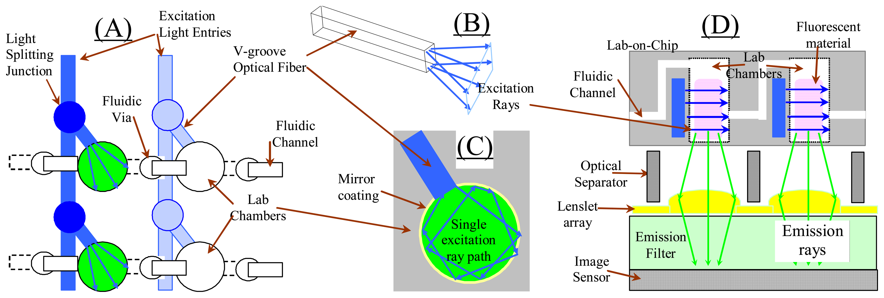
The first method utilizes waveguides for side illumination of the fluorescent material placed into micro-compartments of the lab-on-chip as envisaged in Figure 1.
The waveguides can be integrated with or formed in a body or substrate of the lab-on-chip device. Alternatively, the lab-on-chip device may be manufactured with a plurality of grooves sizewise compatible with waveguides inserted into the grooves. This embodiment is particularly useful when the lab-on-chip device is made of a disposable material and it is desired to keep waveguides for additional uses, once the device is discarded. As shown in Figure 1-A, V-groove optical fibers or simply waveguides are multi-furcated, having a plurality of light-splitting junctions, such that the excitation light enters through a single primary waveguide, and is distributed by light-splitting junctions to secondary waveguide. Each light splitting junction is designed to satisfy the numerical apertures of its outgoing waveguide. Waveguides may also be arranged in several multi-furcated trees, so that the excitation light can enter the device through several primary waveguides, where each tree is dedicated to a particular excitation wavelength.
The waveguides distribute the light in a manner such that the impingement of the excitation light on a fluorescence material is maximized, while the interaction with the light detector, or image sensor, is minimized. This can be better understood from Figure 1-C, D which illustrates a side view (Figure 1-D) and a top view (Figure 1-C) of one waveguide-guiding light into the lab chamber. The minimization of the interaction of the excitation light with the image sensor is achieved by imposing a substantially parallel propagation direction on the excitation light relatively to the surface. The lab chamber comprises a reflective coat covering the walls, reflecting the excitation light and hence, further increasing the impingement of the excitation rays with the fluorescence material.
While the excitation light is constrained to propagate in a predetermined direction (see Figure 1-B), the optical signal, generated by the fluorescent material, propagates in all directions. The bottom side of chamber is not coated and therefore, the optical signal projected onto the image sensor without being screened by the excitation light, is substantially confined in the chamber. It is appreciated, however, that the excitation light can be diverted, for example, when not absorbed by the fluorescence material but rather being scattered to a different direction. Therefore, an emission filter is positioned in the light path of optical signal preventing the diverted rays of excitation light from arriving to the image sensor, while it allows the transmission of the optical signal substantially without loses. The optical signals generated in different reaction chambers are spatially separated so as to prevent cross talks between the different optical signals. The imaging, rather than the signal-intensity measurement, is performed by means of an optical focusing device (e.g., a microlens) in the light path of the optical signal.
We can summarize that the significance of the method is in a high utilization of the excitation energy for a low concentration of the fluorescent material. The secondary significance is a very low excitation background projected into the image sensor.
Transparent μLED chip 180° utilization
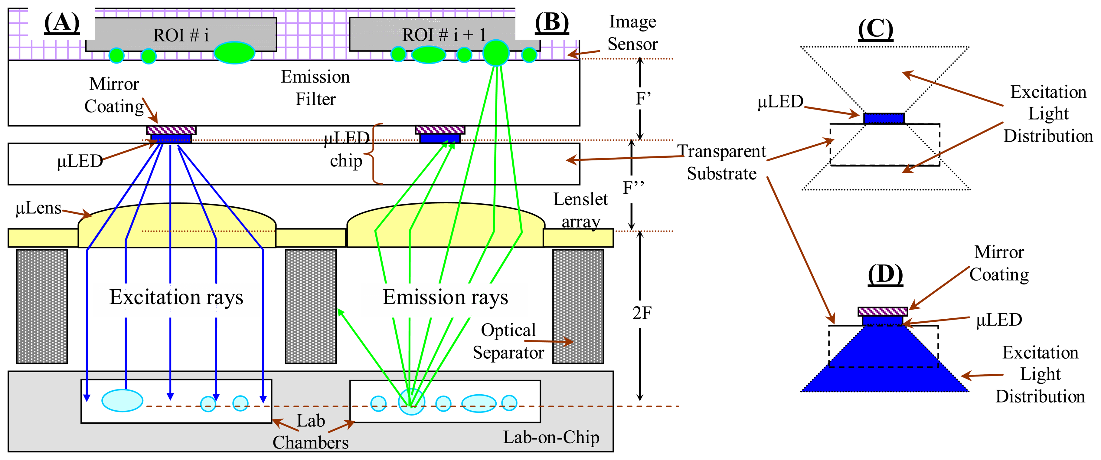
The placement of the transparent “micro Light Emiting Device” (μLED) chip, between the lab-on-chip and the imaging device, allows the placement of the excitation light sources on the same optical axis with the emission detector. The excitation and emission rays are directed controversly as visualized on Figure 2-A,B correspondingly.
The main element of the currently discussed μTAS is a μLEDs chip. It is a matrix of μLEDs grown on a transparent substrate. It is an inexpensive device and could be configured to emit any visible or near infra-red light. Each μLED could be addressable, like a Read Only Memory (RAM), and is therefore activated independently. The arrangements of the μLEDs are compatible with the arrangement of μlenses of a lenslet array. The transverse size of each light-emitting device is typically 15 μm. Dimensions of the μlens correspond to the aperture of the lab chamber and could vary in the range 250 μm – 2 mm. Therefore, the μLED could be referred as a point-light source.
Figure 2-A shows one LED and one lens, respectively. The image sensor is connected to an emission filter preventing randomly reflected excitation rays from penetrating therethrough. The LED generates an excitation light in a direction opposite to the image sensor by means of a reflector. The reflector doubles the excitation intensity as illustrated in Figure 2-C,D. As shown in Figure 2-A, each LED is positioned at the focal point of the corresponding lens, so that the collimated excitation light impinges the fluorescent material located inside the lab chambers by parallel rays.
Figure 2-B shows the light path of the optical emission signals, emitted by the fluorescent material. The same lens is positioned in a manner such that the optical signals are focused by the lens to impinge on the image sensor. The positioning could be half way between the image sensor and lab-on-chip, at two focal distances therefore, providing an unity zoom. Other distances are possible in order to perform an image magnification. Being emitted at a plurality of directions, the most portion of the emission arriving the lens is not affected by reflector.
Spatial filtering of the excitation background
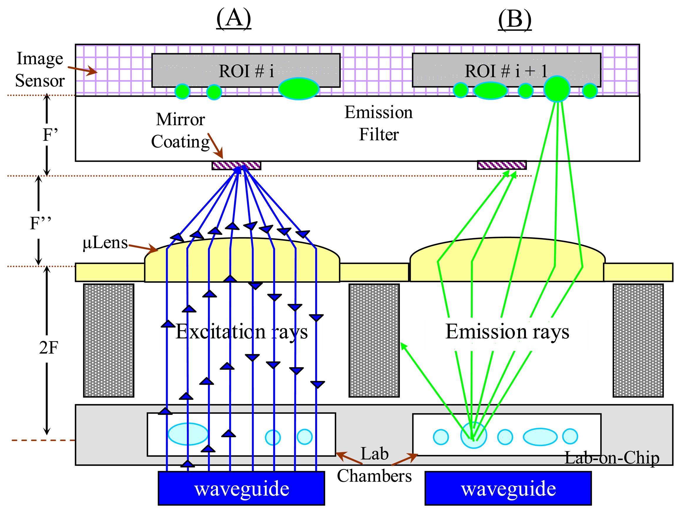
The excitation background spatial filtering (EBSF) method can theoretically completely obstruct the excitation rays to reach the emission detector. It requires excitation light sources providing parallel rays that, for instance, could be carried out from a piggy-tailed optical fibers bundle.
Like in the section before, the μlenses of the lenslet array are used for the separation of the excitation light from the emission signal. This can be better understood from Figure 3, which is a simplified illustration of the excitation and emission lights paths. When the excitation light (see Figure 3-A) enters the lab chamber it can (i) be absorbed by the fluorescence material which in response emits the optical signal; (ii) scatter off the fluorescence material and continue to propagate in a diverted direction; or (iii) continue to propagate in its original direction without interacting with any substance.
The option (iii) is the most prevalent. The lens is positioned in a manner such that the parallel, non-interacting, light rays are concentrated to its focal point. An opaque object or a reflector is positioned in the focal point of the lens, absorbing or reflecting the excitation rays hence preventing them from arriving to the image sensor. The reflector is sufficiently small so as not to absorb or reflect off-focal rays. Unlike the excitation light, the emission signals (see Figure 3-B) are emitted and propagated in a plurality of directions, so that only a small portion is blocked. Being sufficiently small, the effect of reflector is negligible for the emission rays. The excitation rays of low prevalence (kind ii) are absorbed by an emission filter adjacent to the image sensor. The performance could be further improved, placing the excitation filter before the lenslet array, however, it will reduce the mechanical separation of the crosstalk signals.
Discussion
The aforementioned methods were developed for non-specific toxicants detection using a cell on chip concept. One application is for water-toxicity detection. In this application, a genetically engineered bacterium (E. Coli) generating green fluorescent proteins (GFP) was used as biological sensor. The bacteria were uniformly distributed inside the lab chamber, synthesing GFP as a response on a certain analyte exposed to. The biological activity is exponentially faded when the bacteria concentration is above some optimum. Unfortunately, the optimal concentration was a quite low, therefore, the fluorescent signal was very small. Due to the biological constraints, the conventional setup was found as not sensitive enough for a μTAS [11].
Each one of the methods presented in that work was expected to significantly increase the fluorescence signal with regard to the background sensitivity, relatively to conventional techniques used in our research. However, bioluminescence-based biosensors were found as preferable due to a faster detection response for the target analytes. Therefore, the supposed methods were not reduced to practice, since we switched our research activities toward μTAS, based on bioluminescence-based reporters.
Summary and conclusions
In this work three advanced methods for fluorescence based μTAS have been suggested. The significance of the first one is in the high utilization of the excitation energy for low concentrations of the fluorescent material. The utilization of a transparent μLED chip, for the second method, allows the placement of the excitation light sources on the same optical axis with emission detector, such that the excitation and emission rays are directed controversy. The third method presents a spatial filtering of the excitation background.
Despite of that the methods were not implemented, the first one prospected to be the best, since theoretically it utilizes all the excitation energy. However, it requiring more complicated lab-on-chip, since the excitation waveguides should be squeezed with other ingredients such as, for instance, μfluidic channels.
The implementation of any of the proposed methods is not a trivial issue. The selection of the preferable method strongly depends on the application. Although, a practical approach of the suggested method could be a challenging task, our main conclusion is that the set-up must be significantly improved in the performance and effectiveness to achieve a fluorescence-based μTAS.
References
- Thrush, E.; Levi, O.; Ha, W.; Carey, G.; Cook, L.J.; Deich, J.; Smith, S.J.; Moerner, W.E.; Harris, J.S. Integrated semiconductor vertical-cavity surface-emitting lasers and PIN photodetectors for biomedical fluorescence sensing. IEEE J. Quantum Electron. 2004, 40(5), 491. [Google Scholar]
- Thrush, E.; Levi, O.; Ha, W.; Wang, K.; Smith, S.J.; Harris, J.S. Integrated bio-fluorescence sensor. J. Chromatogr. A 2003, 1013(1-2), 103. [Google Scholar]
- Mogensen, K.B.; Klank, H.; Kutter, J.P. Recent developments in detection for microfluidic systems. Electrophoresis 2004, 25(21-22), 3498. [Google Scholar]
- Lagally, E.T.; Mathies, R.A. Integrated genetic analysis microsystems. J. Phys. D-Appl. Phys. 2004, 37(23), R245. [Google Scholar]
- Ruano, J.M.; Glidle, A.; Cleary, A.; Walmsley, A.; Aitchison, J.S.; Cooper, J.M. Design and fabrication of a silica on silicon integrated optical biochip as a fluorescence microarray platform. Biosens. Bioelectron. 2003, 18(2-3), 175. [Google Scholar]
- Webster, J.R.; Burns, M.A.; Burke, D.T.; Mastrangelo, C.H. Monolithic capillary electrophoresis device with integrated fluorescence detector. Anal. Chem. 2001, 73(7), 1622. [Google Scholar]
- Cho, E.J.; Bright, F.V. Optical sensor array and integrated light source. Anal. Chem. 2001, 73(14), 3289. [Google Scholar]
- Chabinyc, M.L.; Chiu, D.T.; McDonald, J.C.; Stroock, A.D.; Christian, J.F.; Karger, A.M.; Whitesides, G.M. An integrated fluorescence detection system in poly(dimethylsiloxane) for microfluidic applications. Anal. Chem. 2001, 73(18), 4491. [Google Scholar]
- Bruno, A.E.; Barnard, S.; Rouilly, M.; Waldner, A.; Berger, J.; Ehrat, M. All-solid state miniaturized fluorescence sensor array for the determination of critical gases and electrolytes in blood. Anal. Chem. 1997, 69(3), 507. [Google Scholar]
- Shacham, Y.; Rabner, A.; Pedhazur, R.; Oksman, M.; Rosen, R.; Benovici, I. Method and system for detecting analytes. Application No. US 53909704, 2004. [Google Scholar]
- Rabner, A. Whole Cell Based Toxicity Detection Integrated System. M.Sc. Thesis, Tel-Aviv University, Israel, 2004. [Google Scholar]
Figure 1.
Side illuminated fluorescence imaging lab-on-chip array.

Figure 2.
Transparent μLED chip 180° utilization with lab-on-chip array.

Figure 3.
Excitation background spatial filtering.

© 2006 by MDPI ( http://www.mdpi.org). Reproduction is permitted for non-commercial purposes.
Share and Cite
MDPI and ACS Style
Rabner, A.; Shacham, Y. A Concept for a Sensitive Micro Total Analysis System for High Throughput Fluorescence Imaging. Sensors 2006, 6, 341-349. https://doi.org/10.3390/S6040341
AMA Style
Rabner A, Shacham Y. A Concept for a Sensitive Micro Total Analysis System for High Throughput Fluorescence Imaging. Sensors. 2006; 6(4):341-349. https://doi.org/10.3390/S6040341
Chicago/Turabian StyleRabner, Arthur, and Yosi Shacham. 2006. "A Concept for a Sensitive Micro Total Analysis System for High Throughput Fluorescence Imaging" Sensors 6, no. 4: 341-349. https://doi.org/10.3390/S6040341