High-temperature MEMS Heater Platforms: Long-term Performance of Metal and Semiconductor Heater Materials

Abstract
:Introduction
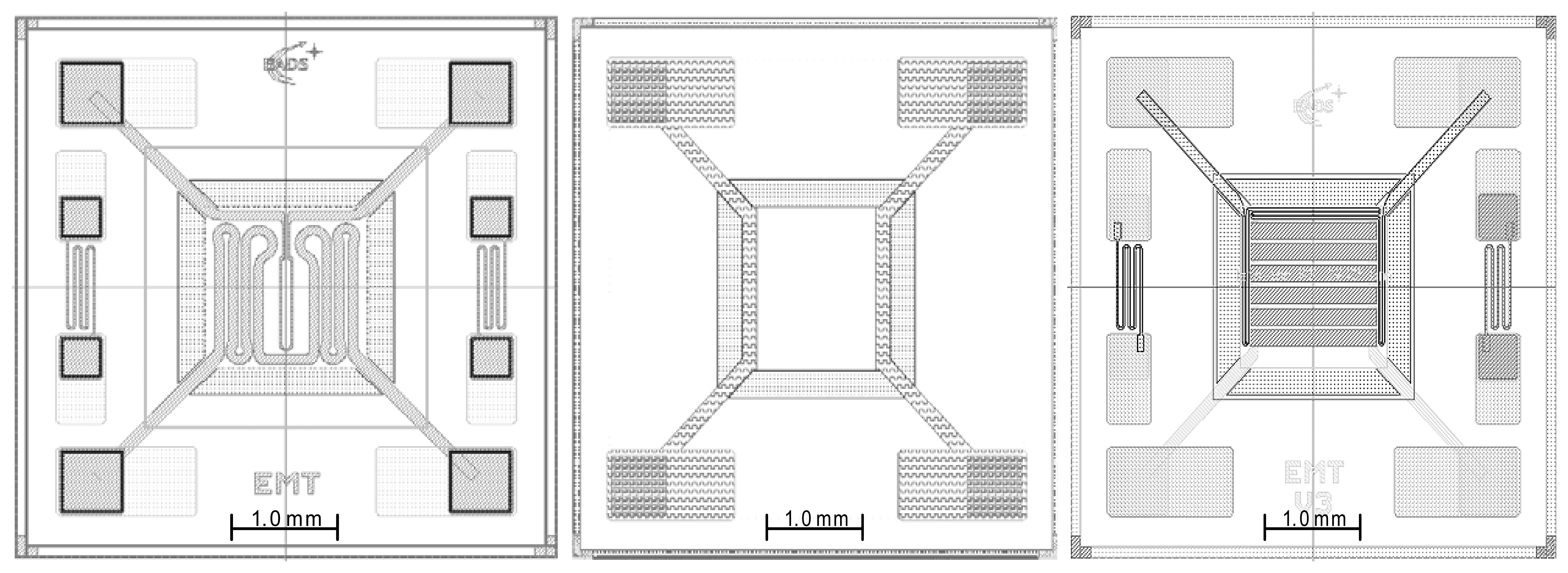
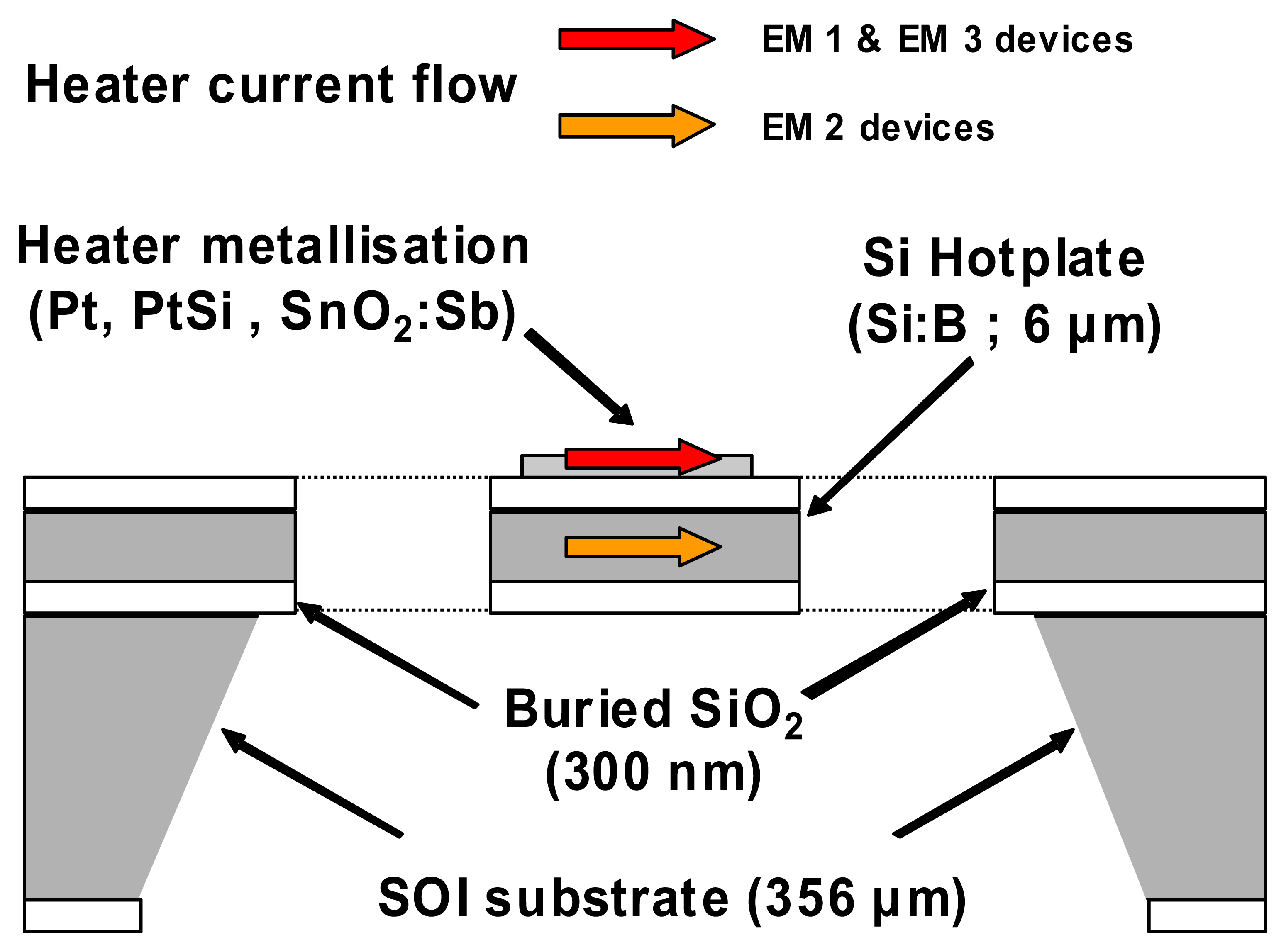
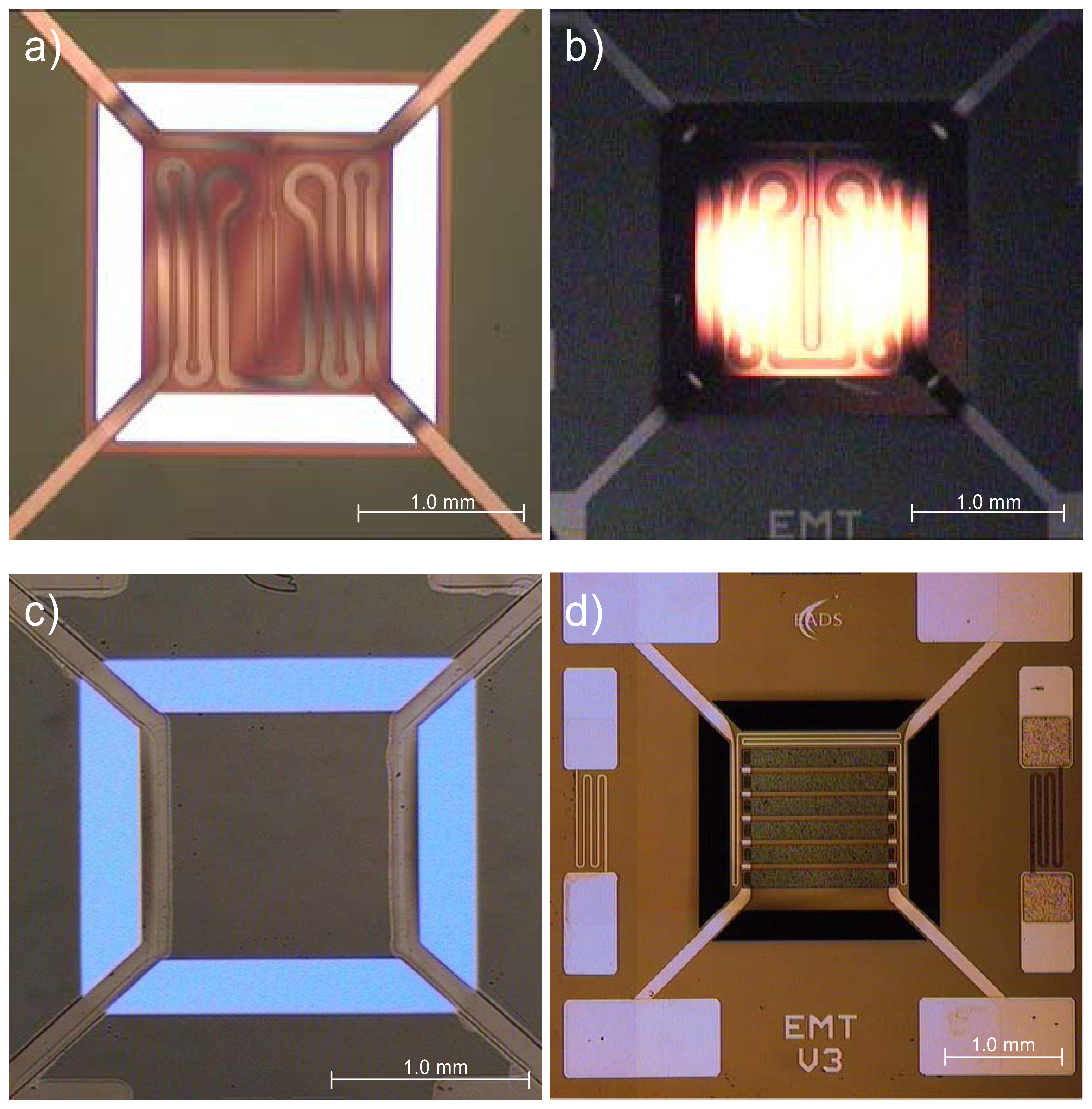
Emitter design
Fabrication
Results and discussions
Heating power consumption
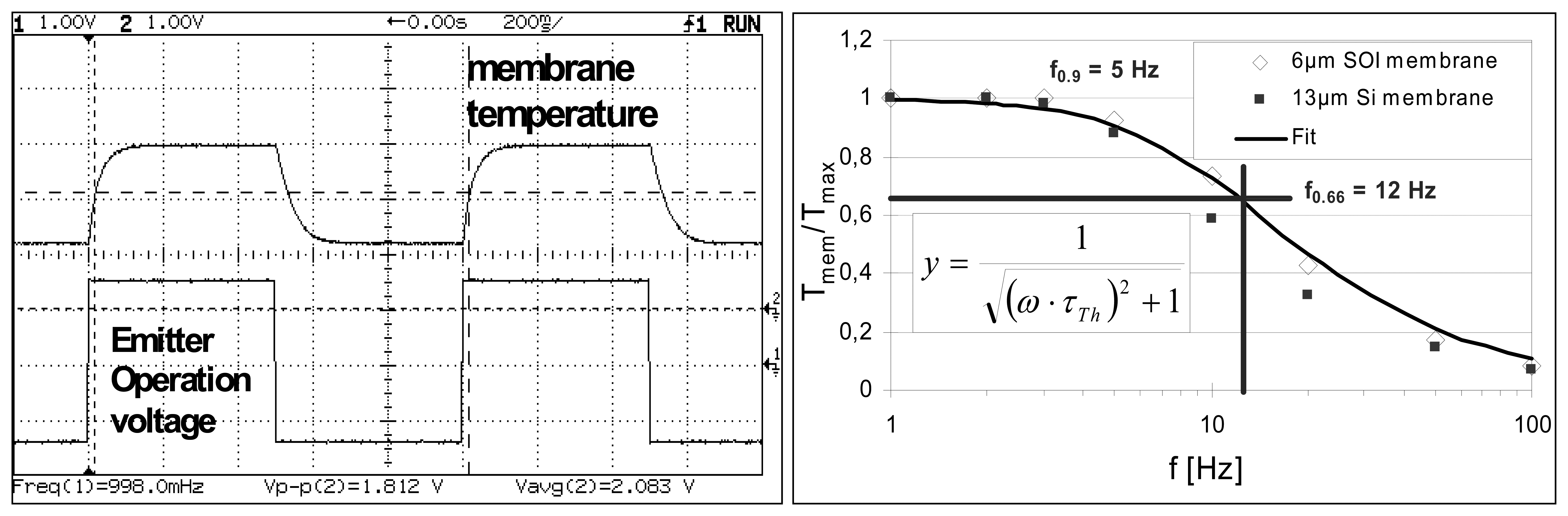
Modulation frequency
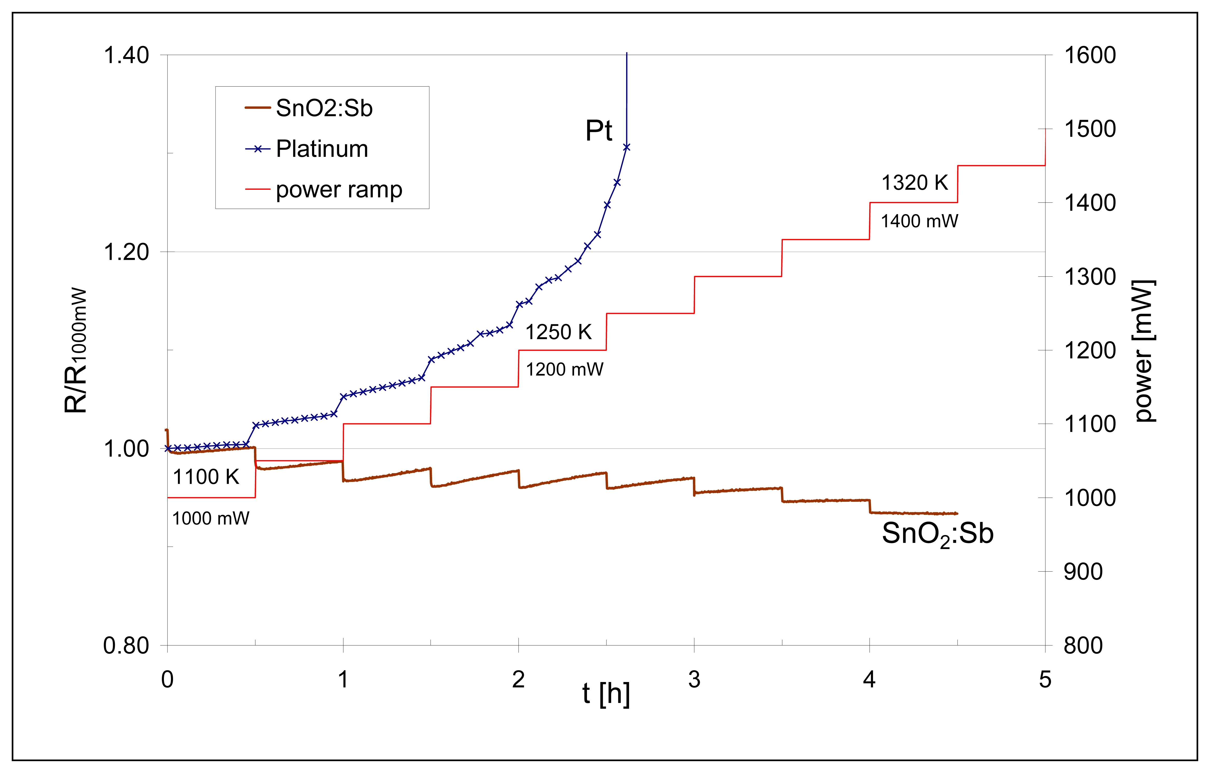
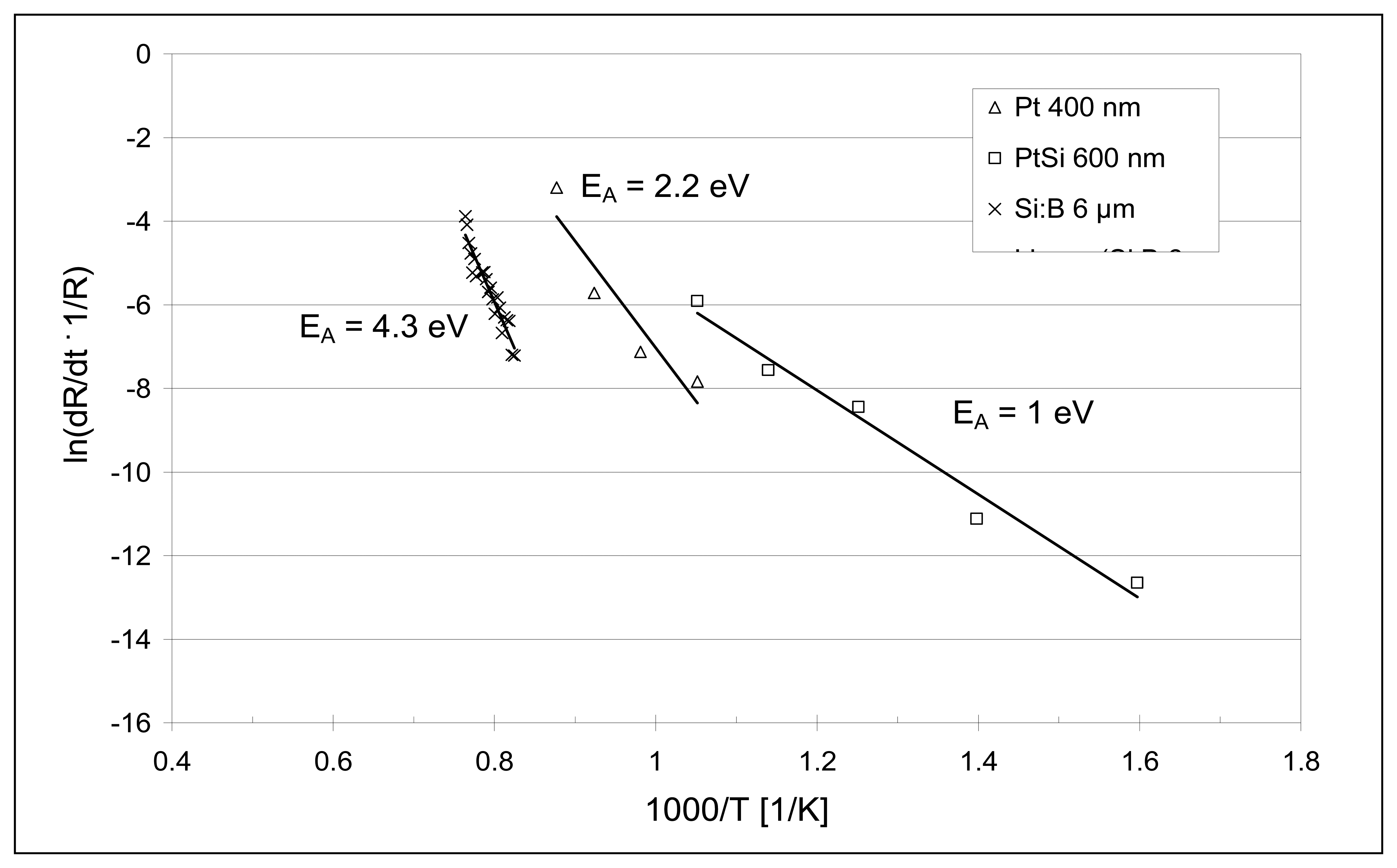
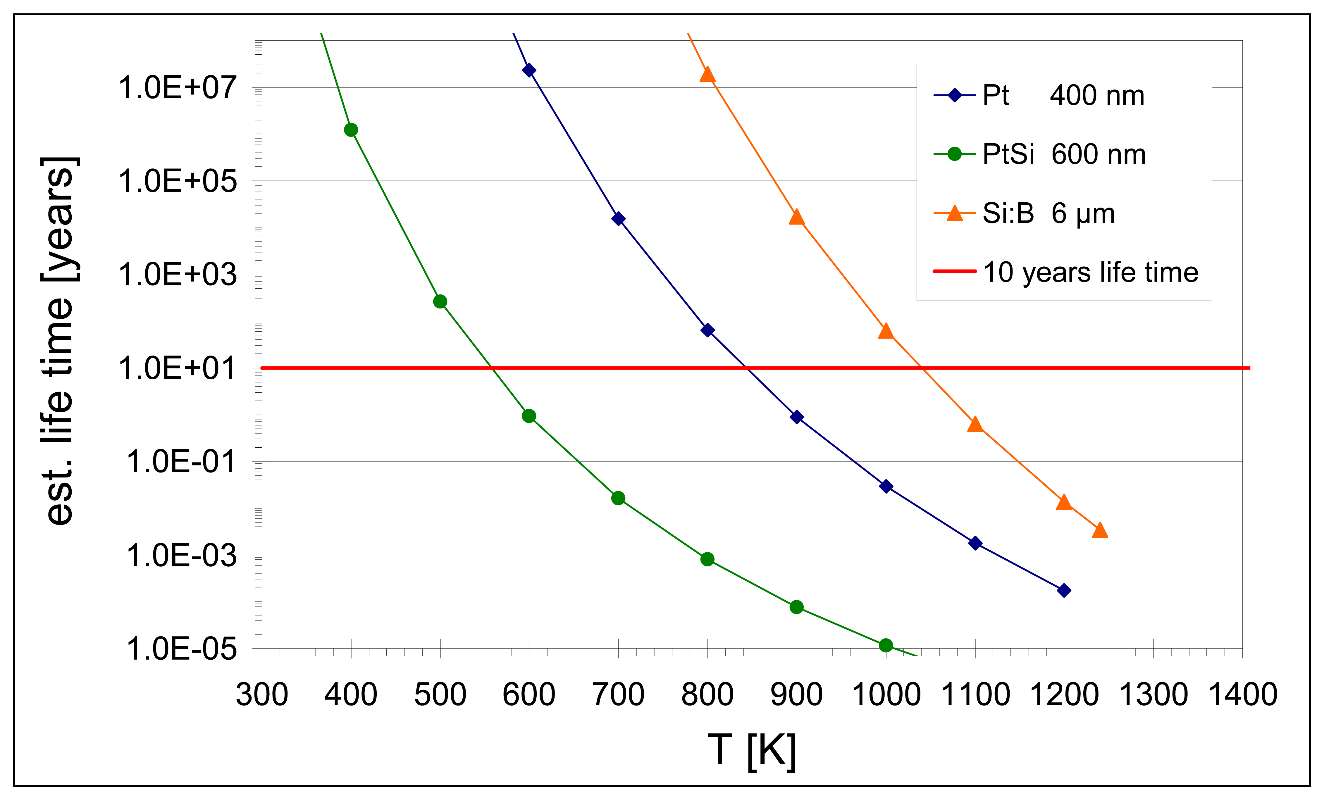
Accelerated degradation tests
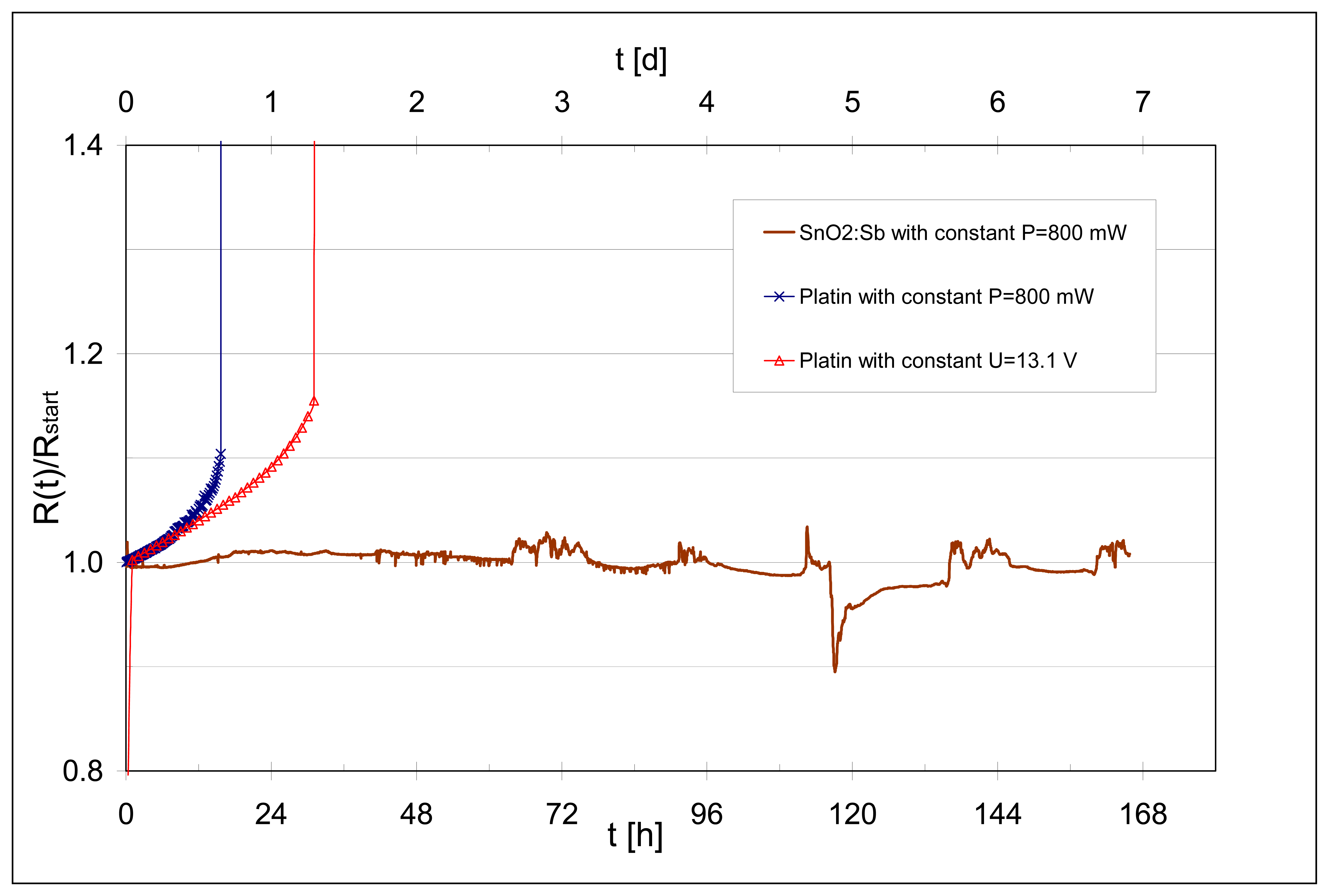
Direct measurement of the long-term stability of heater metallisations
SnO2:Sb based area heater elements
Conclusions
Acknowledgments
References
- Moseley, P.T.; Norris, J.; Williams, D.E. Techniques and Mechanisms in Gas Sensing; Adam Hilger: Bristol, Philadelphia and New York, 1991. [Google Scholar]
- Wöllenstein, J.; Böttner, H.; Jaegle, M.; Becker, W.J.; Wagner, E. Material properties and the influence of metallic catalysts at the surface of highly dense SnO2 films. Sensors & Actuators B 2000, 70, 196. [Google Scholar]
- Bârsan, N. Fundamental and practical aspects in the design of nanoscaled SnO2 gas sensors: a status report. Fresenius J. Anal. Chem. 1999, 365, 287. [Google Scholar]
- Müller, G.; Friedberger, A.; Kreisl, P.; Ahlers, S.; Schulz, O.; Becker, T. A MEMS toolkit for metal-oxide-based gas sensing systems. Thin Solid Films 2003, 436, 34. [Google Scholar]
- Sberveglieri, G.; Hellmich, W.; Müller, G. Silicon hotplates for metal oxide gas sensor elements. Microsystem Technologies 1997, 3, 183. [Google Scholar]
- Heilig, A.; Barsan, N.; Weimar, U.; Göpel, W. Selectivity enhancement of SnO2 gas sensors: simultaneous monitoring of resistances and temperatures. Sensors & Actuators B 1999, 58, 30. [Google Scholar]
- Brand, D.; Krauss, A.; van der Schoot, B.; Weimar, U.; Bârsan, N.; Göpel, W.; de Rooij, N.F. Design and fabrication of high-temperature micro-hotplate for drop-coated gas sensors. Sensors & Actuators B 2000, 68, 223. [Google Scholar]
- Gardner, J.W.; Bartlett, P.N. Electronic noses: Principles and applications; Oxford University Press, 1999. [Google Scholar]
- Gardner, J.W.; Lee, S.M.; Bartlett, P.N.; Guerin, S.; Briand, D.; de Rooij, N.F. Silicon planar microcalorimeter employing nanostructured films. In Transducers 2001; Germany: Munich, Germany, June 10-14 2001. [Google Scholar]
- Kreisl, P.; Helwig, A.; Müller, G.; Obermeier, E.; Sotier, S. Detection of hydrocarbon species using silicon MOS field-effect transistors operated in a non-stationary temperature-pulse mode. Sensors & Actuators B 2005, 106, 442. [Google Scholar]
- Lobert, P.E.; Bourgeois, D.; Pampin, R.; Akheyar, A.; Hagelsieb, L.M.; Flandre, D.; Remacle, J. Immobilization of DNA on CMOS compatible materials. Sensors and Actuators B 2003, 92, 90. [Google Scholar]
- Stankova, M.; Ivanov, P.; Llobet, E.; Brezmes, J.; Vilanova, X.; Gràcia, I.; Cané, C.; Hubalek, J.; Malysz, K.; Correig, X. Sputtered and screen-printed metal oxide-based integrated micro-sensor arrays for the quantitative analysis of gas mixtures. Sensors and Actuators B 2004, 103, 23. [Google Scholar]
- Solzbacher, F.; Imawan, C.; Steffes, H.; Obermeier, E.; Eickhoff, M. A new SiC/HfB2 based low-power gas sensor. Sensors and Actuators B 2001, 77, 111. [Google Scholar]
- Pollien, A.; Baborowski, J.; Ledermann, N.; Muralt, P. New Material for thin film filament of micromachined hot-plate. In Transducers 2001; Munich, Germany, June 10-14 2001. [Google Scholar]
- Yuasa, H.; Ohya, S.; Karasawa, S.; Akimoto, K.; Kodato, S.; Takahashi, K. Single crystal silicon micromachined pulsed infrared light source. In Transducers 1997; Chicago, June 16-19 1997. [Google Scholar]
- Ohlckers, P.; Ferber, A.M.; Dmitriev, V.K.; Kirpilenko, G. A photo-acoustic gas sensing silicon microsystem. In Transducers 2001; Germany: Munich, Germany, June 10-14 2001. [Google Scholar]
- Luthardt, M. Ein flammenloser Ionisationsdetektor. In CLB Chemie in Labor und Biotechnik; Volume 48, Jahrgang, Heft 5, 1997. [Google Scholar]
- Rasulev, U.Kh.; Nazarov, E.G.; Khudaeva, G.B. Chromatographic determination of trace amounts of amines using surface ionization detector. Journal of Chromatography A 1995, 704, 473. [Google Scholar]
- Krötz, G.; Legner, W.; Müller, G.; Grüninger, E.; Smith, L.; Leese, B.; Jones, A.; Rushworth, S. Structural and electronic characterisation of ß-SiC films on Si grown from monomethylsilane precursors. Materials Science and Engineering 1995, B29, 154. [Google Scholar]
- Eickhoff, M.; Möller, H.; Rapp, M.; Krötz, G. Selective growth of high-quality 3C-SiC using a SiO2 sacrificial-layer technique. Thin Solid Films 1999, 345, 197. [Google Scholar]
- Fehlner, F.P. Low temperature oxidation of metals and semiconductors. J. Electrochem. Soc. 1984, 131(7), 1645. [Google Scholar]
- Eickhoff, M. PhD thesis, Technical University of Munich, 1999.
- Sze, S.M. Physics of semiconductor devices; J. Wiley & Sons: New York, 1981. [Google Scholar]
- Landolt-Börnstein Group III Volume 17a Semiconductors: Physics of Group IV Elements and III-V Compounds; Springer-Verlag: Berlin, 1982; ISBN 3-540-10610-3.
- Schulz, O.; Müller, G.; Lloyd, M.; Ferber, A. Impact of environmental parameters on the emission intensity of micromachined infrared sources. Sensors & Actuators A 2005, 121, 172. [Google Scholar]
- Terrier, C.; Chatelon, J.P.; Roger, J.A. Electrical and optical properties of Sb:SnO2 thin films obtained by the sol-gel method. Thin Solid Films 1997, 295, 95. [Google Scholar]
- Friedberger, A.; Kreisl, P.; Rose, E.; Müller, G.; Kühner, G.; Wöllenstein, J.; Böttner, H. Micromechanical fabrication of robust, low-power metal-oxide gas sensors. Sensors and Actuators B 2003, 93, 345. [Google Scholar]
- Castro, M.S.; Aldao, C.M. Characterization of SnO2-varistors with different additives. Journal of the European Ceramic Society 1998, 18, 2233. [Google Scholar]
- Sahar, M.R.; Hasbullah, M. Properties of SnO2 based ceramics. J. Mat. Sci. 1995, 30, 5304. [Google Scholar]
- Grimes, C.A.; Dickey, E.C.; Pishko, M.V. Encyclopedia of Sensors. ISBN 1-58883-056-X.


| Material | Melting point [K] | Oxidation rate [Å/sec at 1273 K] | Specific Resistance [Ω·cm at 300 K] | Expansion coefficient [ppm/K] |
|---|---|---|---|---|
| Si | 1688 | 4 | 2.3·105 | 2.6 |
| Si:B | 1688 | 4 | 5·10-3 | 2.6 |
| SiO2 | 1986 | 0.4 | 1·1014 | 0.5 |
| SiC | 3073 | - | 2·103 - 100 | 6 |
| SnO2:Sb | 2193 | < 0.1 | 10 - 4·10-3 | 1 |
| Pt | 2042 | 1.1·10-5 | 9 |
| Outer chip dimension | 5000 μm |
| Outer membrane dimension | 2000 μm |
| Membrane size | 1500 μm |
| Length of Si suspensions | 350 μm |
| Width of Si suspensions | 150 μm |
| Thickness of Membrane and Si suspensions | 6 μm |
| Pt heater meander (length × width × thickness) | 12000 μm × 100 μm × 0.4 μm |
| SnO2:Sb heater (EM3) | 6 × 2000 μm × 250 μm × 0.95 μm |
© 2006 by MDPI ( http://www.mdpi.org). Reproduction is permitted for non-commercial purposes.
Share and Cite
Spannhake, J.; Schulz, O.; Helwig, A.; Krenkow, A.; Müller, G.; Doll, T. High-temperature MEMS Heater Platforms: Long-term Performance of Metal and Semiconductor Heater Materials. Sensors 2006, 6, 405-419. https://doi.org/10.3390/s6040405
Spannhake J, Schulz O, Helwig A, Krenkow A, Müller G, Doll T. High-temperature MEMS Heater Platforms: Long-term Performance of Metal and Semiconductor Heater Materials. Sensors. 2006; 6(4):405-419. https://doi.org/10.3390/s6040405
Chicago/Turabian StyleSpannhake, Jan, Olaf Schulz, Andreas Helwig, Angelika Krenkow, Gerhard Müller, and Theodor Doll. 2006. "High-temperature MEMS Heater Platforms: Long-term Performance of Metal and Semiconductor Heater Materials" Sensors 6, no. 4: 405-419. https://doi.org/10.3390/s6040405