
A Dual Half-Bridge Converter with Adaptive Energy Storage to Achieve ZVS over Full Range of Operation Conditions

School of Electrical Engineering and Automation, Harbin Institute of Technology, Harbin 150-001, China
*
Author to whom correspondence should be addressed.
Energies 2017, 10(4), 444; https://doi.org/10.3390/en10040444
Submission received: 1 December 2016
/
Revised: 7 March 2017
/
Accepted: 22 March 2017
/
Published: 28 March 2017
(This article belongs to the Collection Smart Grid)
Abstract
:The phase-shifted full-bridge (PSFB) converter is widely employed in high-power applications. However, circulating current, duty-cycle loss, secondary voltage oscillation, and narrow zero-voltage-switching (ZVS) range are the main drawbacks of the conventional PSFB converter. This paper proposes a novel full-bridge converter to improve the performance of the conventional PSFB converter. The proposed converter contains two paralleled half-bridge inverters and an auxiliary inductor on the primary side. The rectifier stage is composed of six diodes connected with the form of full-bridge rectification. This structure allows the stored energy for ZVS operation to change adaptively with duty-cycle. The power can be transferred from the primary side to the secondary side during the whole period. Therefore, the requirement of output filter inductance is reduced and the circulating current is removed. The proposed converter is a good candidate for high power, high voltage and variable input voltage applications. The operation principle and performance are verified on a laboratory prototype.
1. Introduction
The traditional full-bridge DC/DC converter with phase-shifted control can achieve zero-voltage-switching (ZVS) without any additional devices. The switching loss can be significantly reduced. Hence, the converter can achieve high efficiency and power density. These advantages make the phase-shifted full-bridge (PSFB) converter well-suited for high efficiency, power density, and reliability applications [1,2,3,4,5,6]. However, the drawback of the PSFB converter is the dependency of the ZVS characteristic on the load condition: ZVS is lost as load current decreases. Loss of ZVS at light loads results in low efficiency and high electro-magnetic interference (EMI) due to the increase of switching losses [5]. Another drawback is the existence of circulating current, which will significantly increase conduction loss [6]. Extending ZVS range and reducing circulating current are two key areas to improve the PSFB converter’s performance.
Many studies have been proposed to overcome the drawbacks of the traditional PSFB converter. Generally, the ZVS range can be extended by utilizing energy stored in the auxiliary circuits [7,8,9,10]. However, the auxiliary circuits lead to higher circulation current and more conduction loss. The zero-voltage and zero-current-switching (ZVZCS) full-bridge converters are another solution to the problems [11,12,13,14]. In these converters, metal–oxide–silicon field-effect transistors (MOSFETs) as leading-leg switches are turned on with ZVS, while insulated gate bipolar translators (IGBTs) as lagging-lag switches are turned off with ZCS. The ZVS operation is achieved over a wide range of load conditions, and circulating current can be removed by ZCS operation. Generally, these ZVZCS converters result in high secondary-voltage stress and increase the ripple of output voltage. The dual half-bridge converters are a novel solution to extend the ZVS range and remove circulating current [15,16,17]. However, these converters require the specified leakage and magnetizing inductances, which makes the design of transformers complex.
This paper proposes a new dual half-bridge converter with a simple auxiliary circuit. Since the required energy for ZVS increases as duty-cycle decreases, the proposed converter can achieve ZVS operation for all of the primary switches over the entire load range. In addition, the energy from the primary side can be transferred to the output side during the whole switching period, so the output filter requirement is reduced. The proposed converter is well suited for the high-output-voltage applications. Because of these applications, a large filter inductor is required to reduce the ripple current, which results in low efficiency and power density. The operation principle and theoretical analysis are presented to verify these advantages. Experimental results demonstrate the performance of the proposed converter.
2. Operation Principle
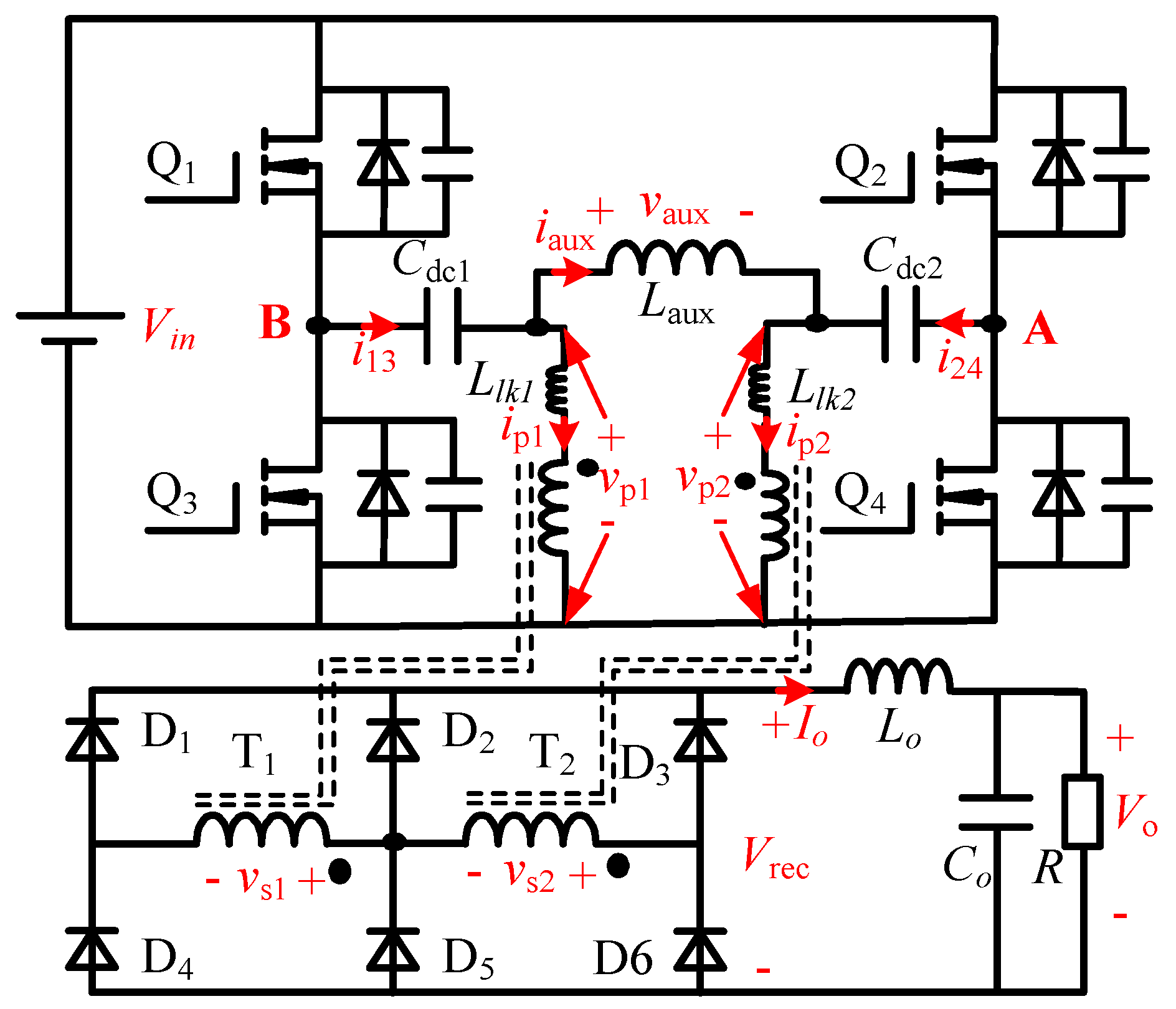
The circuit diagram of the proposed converter is shown in Figure 1. The converter is composed of two half-bridge inverters (HBIs) in parallel, which are driven with phase-shifted control. The transformers of T1 and T2 have the same characteristics with turns ratio of 1:n. Llk1 and Llk2 are the leakage inductances of T1 and T2, respectively. Q1, Q3, Cdc1, and T1 form the lagging-HBI. Q2, Q4, Cdc2, and T2 form the leading-HBI. The auxiliary inductor Laux is used to adaptively adjust the energy for ZVS operation. Two full-bridge rectifiers are employed at the rectifier stage.
For the convenience of circuit analysis, the following assumptions are made:
- (1)
- The blocking capacitors Cdc1, Cdc2 are considered as two constant voltage sources of 0.5Vin.
- (2)
- All the output capacitances of MOSFETs have the same values, Coss.Llk1 and Llk2 also have the same values, Llk.
- (3)
- The output filter inductor Lo is large enough to be treated as a constant current source during a switching period.
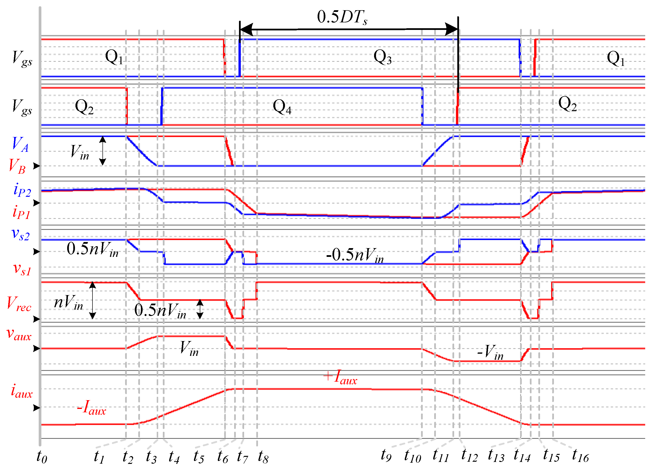
Figure 2 shows the key waveforms of the proposed converter in the steady state. D means the duty-cycle and Ts is the switching period. All the primary switches’ duty-cycles keep constant (50%) if the dead-time is ignored. The output voltage is regulated by adjusting the phase-shift time 0.5DTs between leading-HBI and lagging-HBI. The operating sequence during each switching period can be divided into two half cycles—t0–t8 and t8–t15. Due to the symmetrical structure, only the first half cycle is given. This half cycle can be divided into eight operating modes, whose topological states are shown in Figure 3.
Mode 1 [t0-t1]: Q1 and Q2 are on. The primary voltages of T1 and T2 are 0.5Vin, which leads to the current of Laux keeping negative maximum. The output current Io flows through D3 and D4. Several primary currents are expressed as follows:
Mode 2 [t1-t2]: Q2 is turned off at time t1. The voltage across junction capacitances of Q2 and Q4 are charged and discharged linearly by the constant current source i24(t1). The voltage of point A VA(t) decreases from Vin to 0.5Vin. vs1(t) keeps 0.5nVin and vs2(t) falls from 0.5Vin to zero. Thus, Vrec(t) decreases from nVin to 0.5Vin. The voltage of Laux starts to increase from zero. The voltages in this mode are expressed as:
Mode 3 [t2-t3]: When VA(t) becomes 0.5Vin in Mode 2, vs2(t) falls to zero and D2 starts to conduct. vs2(t) is maintained at zero since D2 and D3 are in conducting state during this mode. The resonance between Llk2 and the junction capacitances occurs. The capacitances are charged or discharged by the energy stored in Llk2. VA(t) decrease from 0.5Vin to zero with a resonance waveform. The voltage of Laux continuously increases. The currents and voltages are expressed as follows:
where .
Mode 4 [t3-t4]: VA(t) reaches zero at time t3 and the parasitic diode of Q4 starts to conduct. Q4 can be turned on with zero voltage in this mode. vs2(t) is maintained at zero and the commutation between D2 and D3 is progressed during this mode. The voltage of Laux rises to Vin. The primary current of T2 is expressed as:
Mode 5 [t4-t5]: Mode 5 begins when ip2(t) falls to zero. The commutation between D2 and D3 is completed at t4. vs2(t) becomes −0.5nVin and T2 stops to transfer the power from input side to output side. The voltage of Laux and Vrec(t) are continuously maintained at Vin and 0.5nVin, respectively. The current of Laux is given by:
Mode 6 [t5-t6]: Q1 is turned off at t5. At the same time, the commutation between D4 and D6 isprogressed. The resonance of junction capacitances and leakage inductances occurs. VB(t) is decreased from Vin to zero and Vrec(t) falls to zero. The current of Laux can be considered to increase to the positive maximum (+Iaux). The primary currents of T1 and T2 are expressed as follows:
Mode 7 [t6-t7]: Mode 7 begins when VB(t) falls to zero. The body diode of Q3 starts to conduct and Q3 can be turned on with zero voltage. vs1(t) and vs2(t) are maintained zero in this mode. The voltage across Llk1 or Llk2 equals to −0.5Vin. The commutation between D4 and D6 is continually progressed. The currents are expressed as follows:
Mode 8 [t7-t8]: Mode 8 begins when ip1(t) falls to zero and D4 is naturally turned off. At the same time, vs2(t) becomes −0.5nVin and vs1(t) becomes zero since the commutation between D1 and D2 starts. The voltage across Llk1 is −0.5Vin and ip1(t) decreases linearly.
Mode 8 ends when ip1(t) reaches nIo and D2 is naturally turned off. The commutation between D1 and D2 ends at t8. The power is transferred from the primary side to the secondary side through T1 and T2. The voltage across Laux is zero and iaux is maintained at the positive maximum.
3. Analysis of the Proposed Converter
3.1. Voltage Gain Analysis
Since the durations of duty-cycle loss and dead-time are very narrow, they can be ignored to simplify analysis. Figure 4a shows the simplified rectifier output voltage in the proposed converter. The voltage gain is derived from the volt-second balance of the output filter inductor, and it can be expressed as follows:
The rectifier output voltage waveform in the conventional full-bridge converter is shown in Figure 4b. It can be noted that the energy from the primary side cannot be transferred to the secondary side during freewheel period. For the proposed converter, the energy can always be transferred to the output side during the whole period. Therefore, the filter requirement can be significantly less and the power loss can also be reduced.
As shown in Figure 4b, the voltage of the output filter inductor is nVin − Vo during the duty-cycle period, while the value is −Vo during the freewheeling period. The output filter inductor for the conventional full-bridge converter is calculated based on the given current ripple.
where ΔIout is the current ripple of Lo. In general, ΔIout is set at 20 percent of full load current.
For the proposed converter, the voltage applied on Lo is 0.5nVin − Vo during the freewheeling period. The filter inductor for the proposed converter is calculated as
Figure 5 shows the relationship between the required value of filter inductor and duty-cycle. It can be noted that the filter inductance of the proposed converter is much smaller than that of the traditional full-bridge converter. Therefore, the proposed converter benefits from the reduction of the inductor’s size and copper loss.
3.2. ZVS Characteristics
For the ZVS of leading-HBI switches, the transition is accomplished in Mode 2 and Mode 3. During Mode 2, the output filter inductor takes part in the transition and the voltage of leading-leg is decreased from Vin to 0.5Vin. Then, the transformer is shorted and the remaining voltage falls by the resonance between junction capacitances and leakage inductance of the transformer during Mode 3. The required energy for ZVS can be obtained according to (3)
When the lagging-HBI switch is turned off during Mode 6, the transformers are shorted and only the energies stored in the leakage inductances can be available for lagging-leg transition. According to the Equation (6), the ZVS condition of lagging-leg switches can be expressed as
According to Equations (11) and (12), the ZVS energies are related to Iaux. If the durations of duty-cycle loss and dead-time are ignored, Iaux can be calculated as
According to Equation (13), Iaux and duty-cycle have an inverse relationship. When D is low (e.g., increasing the input voltage or decreasing the load current), the maximum value of auxiliary inductor current will increase. Sufficient energy can be stored in the leakage inductances to achieve ZVS operation. Therefore, the proposed converter can achieve ZVS over the full range of load conditions.
4. Experimental Results
A prototype was built to demonstrate the performance of the proposed converter. The components used in the prototype are shown in Table 1. The circuit parameters of the prototype are given as follows:
- (1)
- Input voltage: Vin = 200–300 V
- (2)
- Output voltage: Vo = 150 V
- (3)
- Maximum output current Io(max) = 5 A
- (4)
- Switching frequency: fs = 80 kHz
The digital-signal-processor (DSP) TMS320F28027 (Texas Instruments, Dallas, TX, USA) was adopted for the digital control of the proposed converter. SPW20N60C3 (Infineon Technologies, Munich, Germany) were used as the primary switches, and the effective output capacitance was 160 pF [18]. The rectifier was formed by IDH08SG60C (Infineon Technologies, Munich, Germany). The input power was evaluated through DC Power Supply 62150H, and the output power was measured through DC Electronic Load 63204, manufactured by the Chroma Company (Taiwan, China).
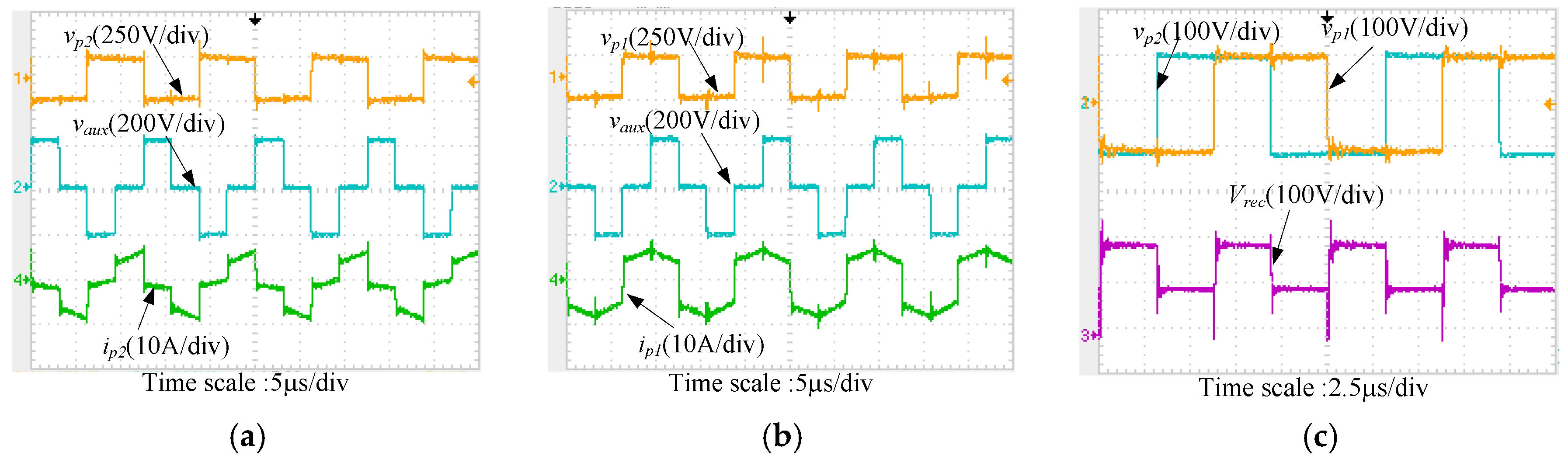
Figure 6 shows the key waveforms of the proposed converter at Vin = 230 V, Io = 5 A. It can be noted that the experimental waveforms coincide well with the theoretical analysis described in Figure 3.
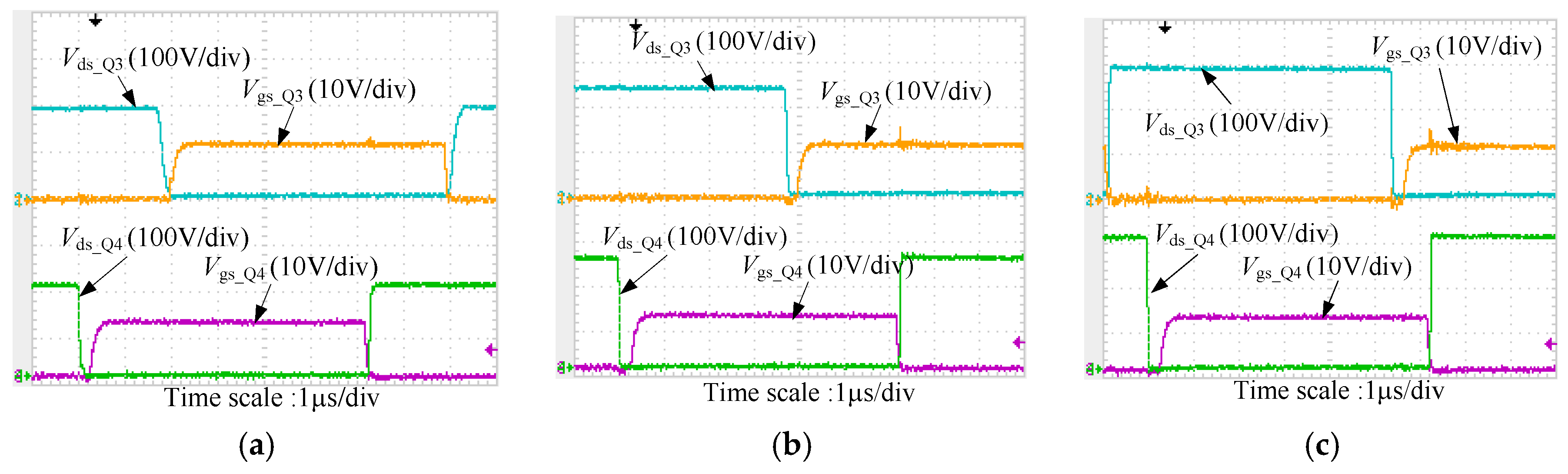
Figure 7 shows the key waveforms of the auxiliary inductor when the proposed converter operates at different duty-cycles. As shown in Figure 7, both the maximum current value of the auxiliary inductor and the available energy for ZVS operation are increased when duty-cycle is decreased. This characteristic is helpful to realize the ZVS under all kinds of operation conditions and can reduce the conduction loss caused by the auxiliary circuit.
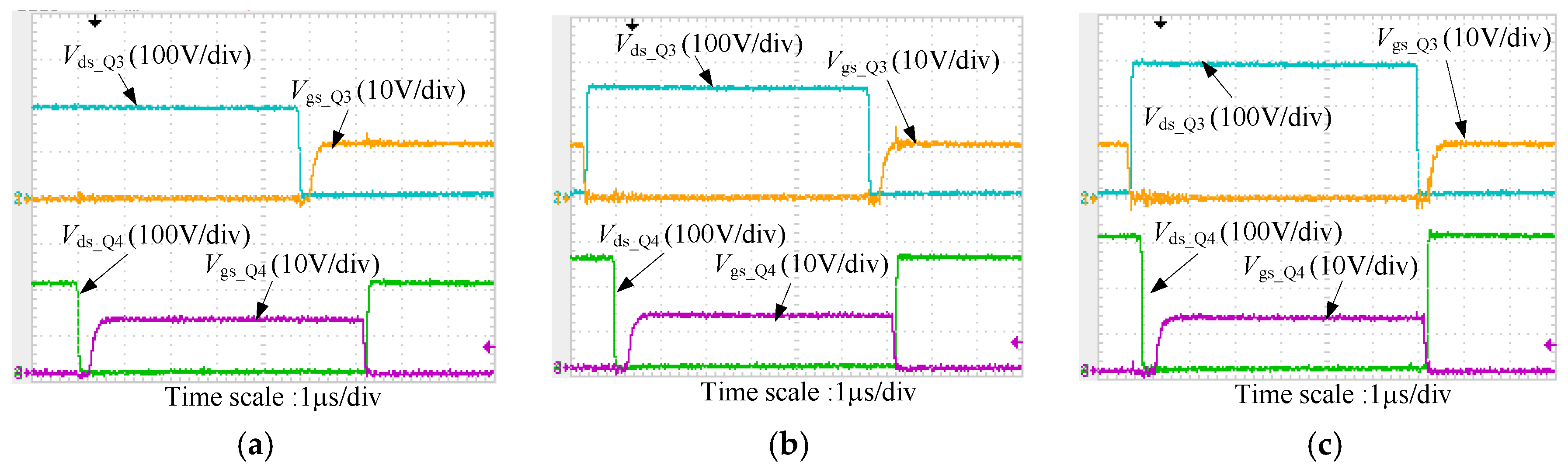
Figure 8 and Figure 9 show the gate-source and drain-source voltage waveforms at Io = 1 A and Io = 50 mA, respectively. It can be noted that all the switches in the proposed converter can achieve ZVS operation over the entire load current and input voltage ranges.
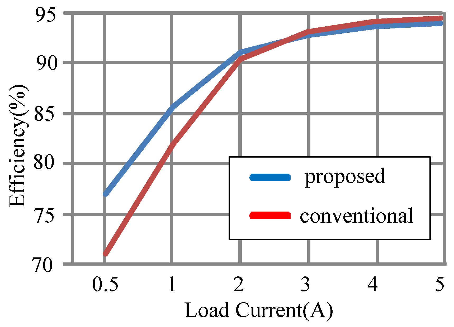
In order to compare the performances, a conventional PSFB converter was built with an external inductance of 20 µH to achieve the ZVS operation over a load range from 50% to 100%. Figure 10 shows the experimental efficiencies of the proposed converter and the conventional converter under different load currents. At heavy loads, both converters could achieve ZVS, while the additional components in the proposed converter increased the conduction losses. Therefore, the efficiency of the proposed converter was a little lower than that of the conventional converter. At light loads, the switching losses were dominant and the conventional converter failed to obtain ZVS. The proposed converter could maintain the ZVS operation and achieve higher efficiency at light loads, as shown in Figure 10. The efficiency improvement was determined by the saved switching losses.
5. Conclusions
A dual half-bridge converter with an auxiliary inductor was proposed to solve the drawbacks of the conventional PSFB converters. The proposed converter can transfer the power from the primary side to the secondary side during the whole period. Therefore, the circulating current is removed and the filter requirement is reduced. The ZVS energy can be changed with the duty-cycle, which is helpful for the realization of ZVS under the whole range of operation conditions. The experimental results coincide with the theoretical analysis. The proposed converter is a good candidate for high power, high voltage, and variable input voltage applications.
Acknowledgments
This work was supported by National Natural Science Foundation (Grant No.51577039).
Author Contributions
Lei Zhao was responsible for the theoretical derivation and paper writing. Haoyu Li and Xuemei Zheng proposed the main idea and analysis method. Chuangyu Xu carried out the simulation and verification.
Conflicts of Interest
The authors declare no conflict of interest.
References
- Kim, Y.D.; Cho, K.M.; Kim, D.-Y.; Moon, G.-W. Wide-range ZVS phase-shift full-bridge converter with reduced conduction loss caused by circulating current. IEEE Trans. Power Electron. 2013, 28, 3308–3316. [Google Scholar] [CrossRef]
- Hu, S.; Li, X.; Lu, M.; Luan, B.-Y. Operation modes of a secondary-side phase-shifted resonant converter. Energies 2015, 8, 12314–12330. [Google Scholar] [CrossRef]
- Kim, J.W.; Kim, D.Y.; Kim, C.E.; Moon, G.W. A simple switching control technique for improving light load efficiency in a phase-shifted full-bridge converter with a server power system. IEEE Trans. Power Electron. 2014, 29, 1562–1566. [Google Scholar] [CrossRef]
- Kim, D.Y.; Kim, C.E.; Moon, G.W. Variable delay time method in the phase-shifted full-bridge converter for reduced power consumption under light load conditions. IEEE Trans. Power Electron. 2013, 28, 5120–5127. [Google Scholar] [CrossRef]
- Zhao, L.; Li, H.; Hou, Y.; Yu, Y. Operation analysis of a phase-shifted full-bridge converter during the dead-time interval. IET Power Electron. 2016, 9, 1777–1783. [Google Scholar] [CrossRef]
- Chen, B.Y.; Lai, Y.S. Switching control technique of phase-shift-controlled full-bridge converter to improve efficiency under light-load and standby conditions without additional auxiliary components. IEEE Trans. Power Electron. 2010, 25, 1001–1012. [Google Scholar] [CrossRef]
- Borage, M.; Tiwari, S.; Kotaiah, S. A passive auxiliary circuit achieves zero-voltage-switching in full-bridge converter over entire conversion range. IEEE Trans. Power Electron. 2005, 3, 141–143. [Google Scholar] [CrossRef]
- Borage, M.; Tiwari, S.; Bhardwaj, S.; Kotaiah, S. A full-bridge DC-DC converter with zero-voltage-switching over the entire conversion range. IEEE Trans. Power Electron. 2008, 4, 1743–1750. [Google Scholar] [CrossRef]
- Safaee, A.; Jain, P.; Bakhshai, A. A ZVS pulse width modulation full-bridge converter with a low-RMS-current resonant auxiliary circuit. IEEE Trans. Power Electron. 2016, 31, 4031–4047. [Google Scholar] [CrossRef]
- Jang, Y.; Jovanovic, M.M. A new PWM ZVS full-bridge converter. IEEE Trans. Power Electron. 2007, 22, 987–994. [Google Scholar] [CrossRef]
- Gu, B.; Lai, J.S.; Kees, N.; Zheng, C. Hybrid-switching full-bridge DC–DC converter with minimal voltage stress of bridge rectifier, reduced circulating losses, and filter requirement for electric vehicle battery chargers. IEEE Trans. Power Electron. 2013, 28, 1132–1144. [Google Scholar] [CrossRef]
- Wu, X.; Xie, X.; Zhao, C.; Qian, Z.; Zhao, R. Low voltage and current stress ZVZCS full bridge DC-DC converter using center tapped rectifier reset. IEEE Trans. Ind. Electron. 2008, 55, 1470–1477. [Google Scholar] [CrossRef]
- Wang, J.; Ji, B.; Wang, H.; Chen, N.; You, J. An inherent zero-voltage and zero-current-switching full-bridge converter with no additional auxiliary circuits. J. Power Electron. 2015, 15, 610–620. [Google Scholar] [CrossRef]
- Seok, K.; Kwon, B. An improved zero-voltage and zero-current-switching full-bridge PWM converter using a simple resonant circuit. IEEE Trans. Ind. Electron. 2001, 48, 1205–1209. [Google Scholar] [CrossRef]
- Lee, I.O.; Moon, G.W. Soft-switching DC/DC converter with a full ZVS range and reduced output filter for high-voltage applications. IEEE Trans. Power Electron. 2013, 28, 112–122. [Google Scholar] [CrossRef]
- Lee, I.O.; Moon, G.W. Phase-shifted PWM converter with a wide ZVS range and reduced circulating current. IEEE Trans. Power Electron. 2013, 28, 908–919. [Google Scholar] [CrossRef]
- Ye, Z.Y. Dual half-bridge DC-DC converter with wide-range ZVS and zero circulating current. IEEE Trans. Power Electron. 2013, 28, 3276–3286. [Google Scholar] [CrossRef]
- SPW20N60C3 Datasheet; Infineon Technologies AG: Munich, Germany, 2010.
Figure 1.
Proposed dual half-bridge converter.

Figure 2.
Key operating waveforms.

Figure 3.
Topological stages of the proposed converter: (a) Mode 1 [t0-t1]; (b) Mode 2 [t1-t2]; (c) Mode 3 [t2-t3]; (d) Mode 4 [t3-t4]; (e) Mode 5 [t4-t5]; (f) Mode 6 [t5-t6]; (g) Mode 7 [t6-t7]; (h) Mode 8 [t7-t8].
Figure 3.
Topological stages of the proposed converter: (a) Mode 1 [t0-t1]; (b) Mode 2 [t1-t2]; (c) Mode 3 [t2-t3]; (d) Mode 4 [t3-t4]; (e) Mode 5 [t4-t5]; (f) Mode 6 [t5-t6]; (g) Mode 7 [t6-t7]; (h) Mode 8 [t7-t8].
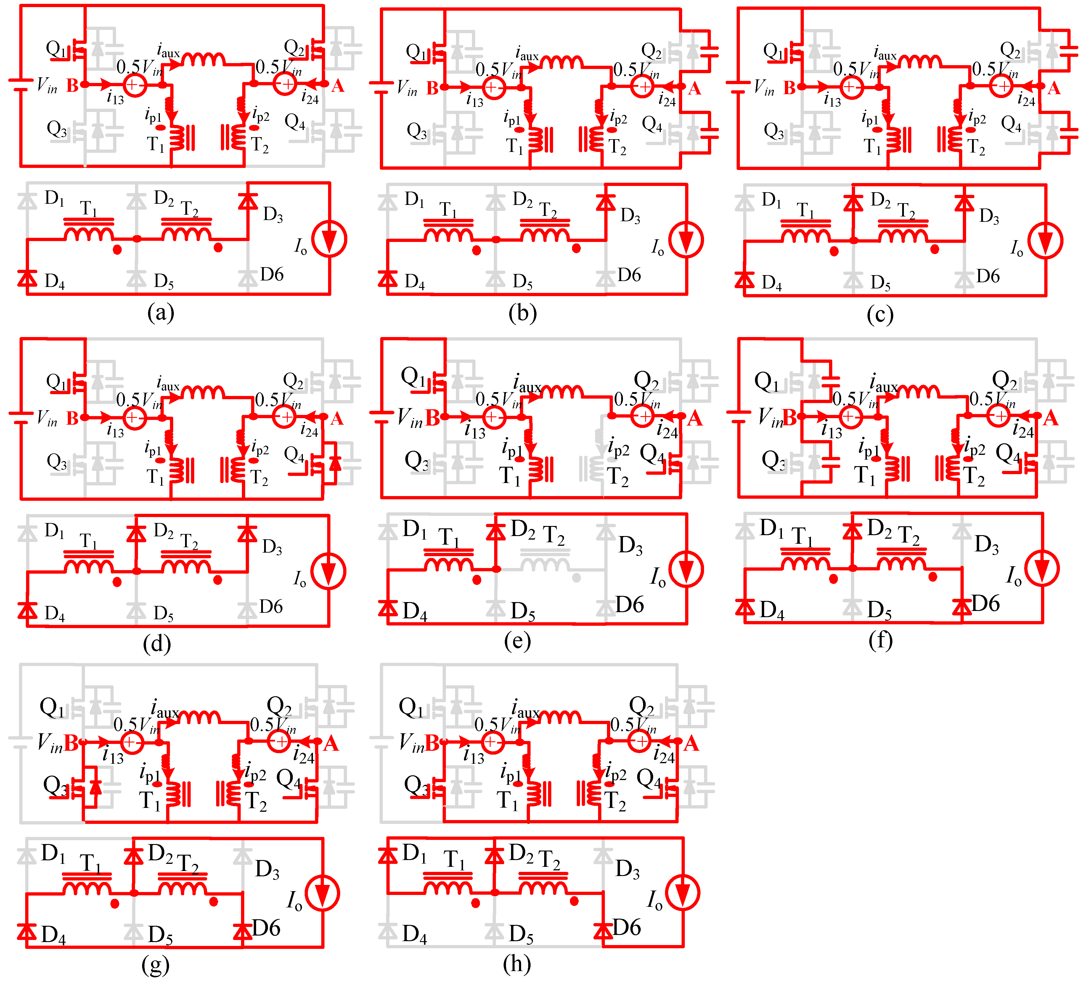
Figure 4.
Idealized rectifier voltage: (a) proposed converter; (b) conventional converter.
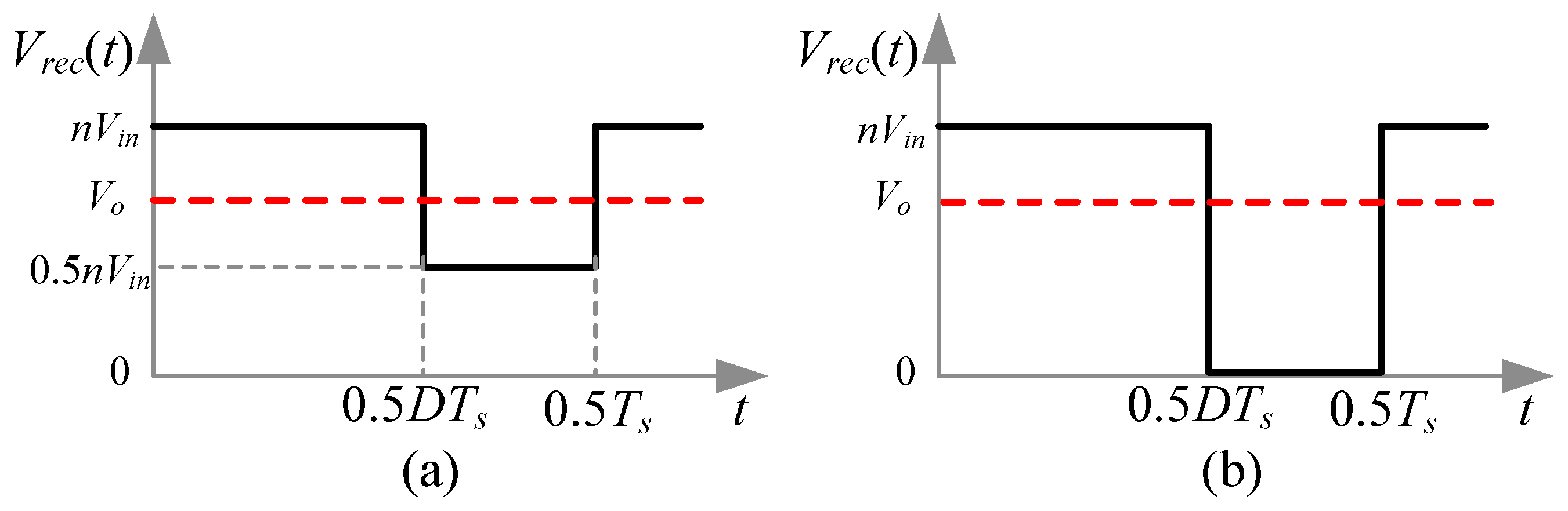
Figure 5.
Filter inductance versus duty-cycle.
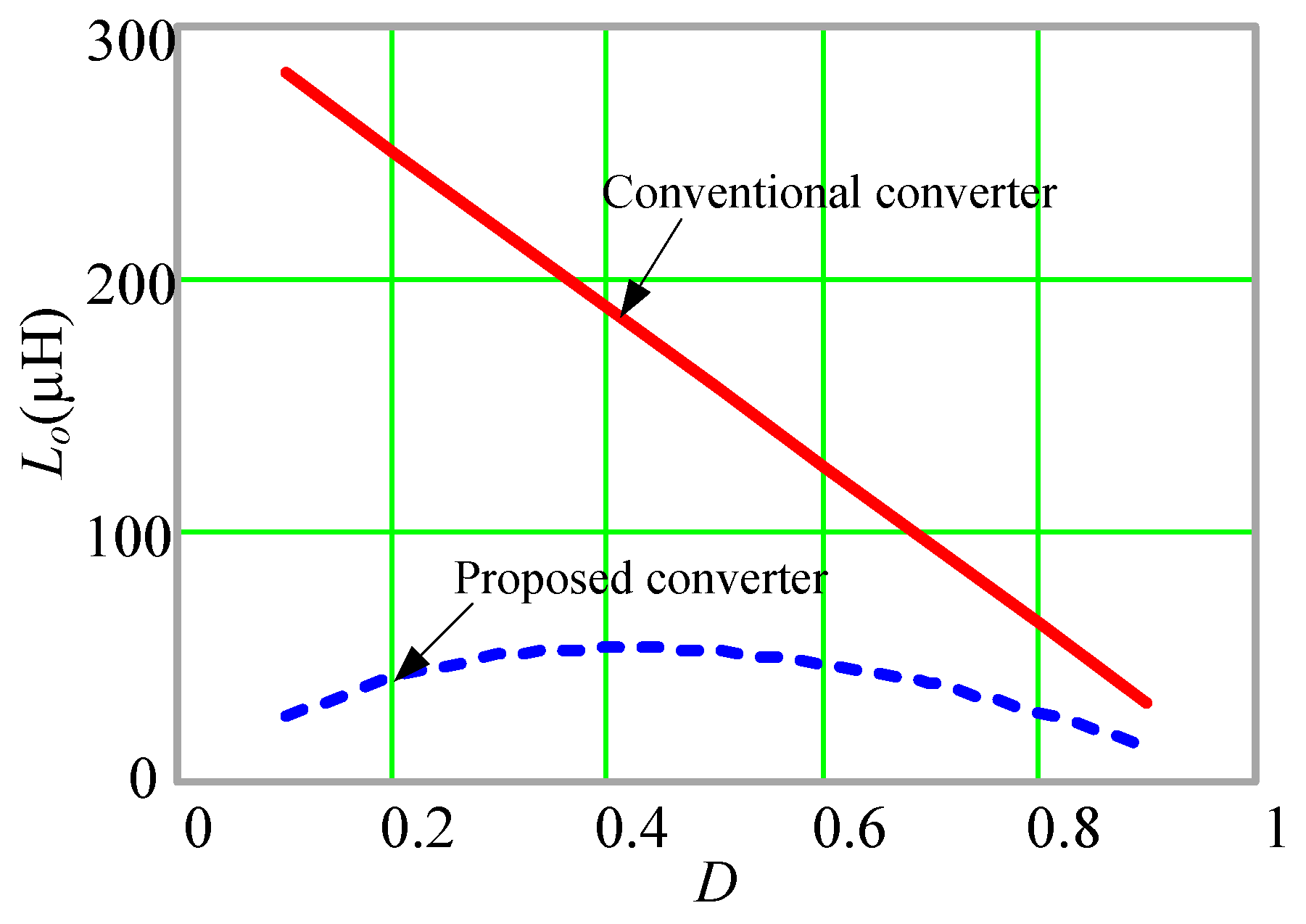
Figure 6.
Key experimental waveforms of the proposed converter at Vin = 230 V and Io = 5 A: (a) leading-half-bridge inverter (HBI); (b) lagging-HBI; (c) primary voltages of two HBIs and rectifier voltage.
Figure 6.
Key experimental waveforms of the proposed converter at Vin = 230 V and Io = 5 A: (a) leading-half-bridge inverter (HBI); (b) lagging-HBI; (c) primary voltages of two HBIs and rectifier voltage.

Figure 7.
Experimental waveforms at different input voltages: (a) Vin = 310 V, D = 0.1; (b) Vin = 250 V, D = 0.5; (c) Vin = 190 V, D = 0.9.
Figure 7.
Experimental waveforms at different input voltages: (a) Vin = 310 V, D = 0.1; (b) Vin = 250 V, D = 0.5; (c) Vin = 190 V, D = 0.9.
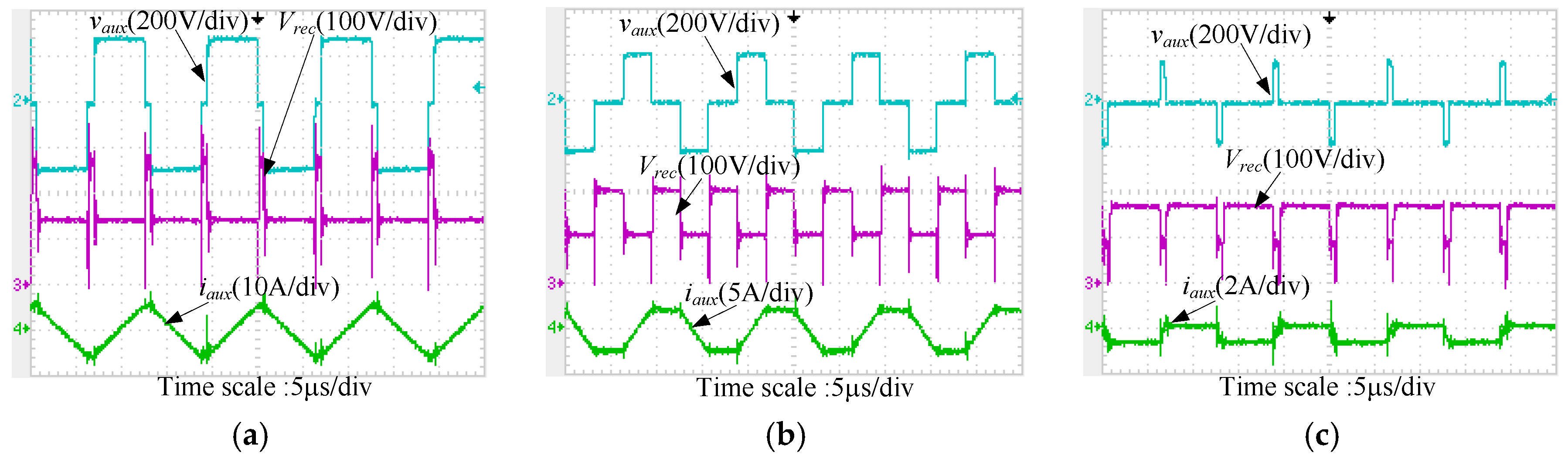
Figure 8.
Zero-voltage-switching (ZVS) waveforms at Io = 1 A: (a) Vin = 200 V; (b) Vin = 250 V; (c) Vin = 300 V.
Figure 8.
Zero-voltage-switching (ZVS) waveforms at Io = 1 A: (a) Vin = 200 V; (b) Vin = 250 V; (c) Vin = 300 V.

Figure 9.
ZVS waveforms at Io = 50 mA: (a) Vin = 200 V; (b) Vin = 250 V; (c) Vin = 300 V.

Figure 10.
Comparison of the converter efficiency.

Table 1.
Components list.
| Main switches (Q1–Q4) | SPW20N60C3 |
| Rectifier diodes (D1–D6) | IDH08SG60C |
| Blocking capacitor (Cdc1Cdc2) | 10 µF |
| Main transformers (T1 T2) | Core PQ3535 Turns ratio n = 0.9 Llk1 = Llk2 = 12 µH |
| Output inductor (Lo) | 60 µH |
© 2017 by the authors. Licensee MDPI, Basel, Switzerland. This article is an open access article distributed under the terms and conditions of the Creative Commons Attribution (CC BY) license (http://creativecommons.org/licenses/by/4.0/).
Share and Cite
MDPI and ACS Style
Zhao, L.; Xu, C.; Zheng, X.; Li, H. A Dual Half-Bridge Converter with Adaptive Energy Storage to Achieve ZVS over Full Range of Operation Conditions. Energies 2017, 10, 444. https://doi.org/10.3390/en10040444
AMA Style
Zhao L, Xu C, Zheng X, Li H. A Dual Half-Bridge Converter with Adaptive Energy Storage to Achieve ZVS over Full Range of Operation Conditions. Energies. 2017; 10(4):444. https://doi.org/10.3390/en10040444
Chicago/Turabian StyleZhao, Lei, Chuangyu Xu, Xuemei Zheng, and Haoyu Li. 2017. "A Dual Half-Bridge Converter with Adaptive Energy Storage to Achieve ZVS over Full Range of Operation Conditions" Energies 10, no. 4: 444. https://doi.org/10.3390/en10040444
Note that from the first issue of 2016, this journal uses article numbers instead of page numbers. See further details here.