GPS Synchronization of Smart Distributed Converters for Microgrid Applications
by
 , and
, and
Tarek A. Youssef
1 ,
,
Aboubakr Salem
2,*,
Moataz Elsied
3,4,
Augustin Mpanda Mabwe
3,
Mohammad Ali Yousef Abido
2 and
Osama A. Mohammed
1
1
Energy Systems Research Laboratory, Department of Electrical and Computer Engineering, Florida International University, Miami, FL 33174, USA
2
Electrical Engineering Department, King Fahd University of Petroleum and Minerals, Dhahran 31261, Saudi Arabia
3
Graduate School of Electronic and Electrical Engineering, Amiens 80080, France
4
Department of Electrical Power and Machines, Helwan University, Helwan 11795, Cairo, Egypt
*
Author to whom correspondence should be addressed.
Energies 2018, 11(4), 695; https://doi.org/10.3390/en11040695
Submission received: 6 February 2018
/
Revised: 12 March 2018
/
Accepted: 14 March 2018
/
Published: 21 March 2018
(This article belongs to the Section F: Electrical Engineering)
Abstract
:In this paper, a smart distributed DC/DC converter synchronization advanced technique and phase angle optimization algorithm are proposed using to reduce the DC bus overall ripple. A global positioning system-based scheme is used to synchronize the carrier among the distributed converters. The carrier phase angle optimization among the different converters is inspired by Carrier-Sense Multiple Access protocol. The proposed system is simulated and analyzed using Matlab/Simulink program. As a proof of concept of the proposed technique, two case studies have been investigated under equal and unequal load sharing among the distributed generators. The proposed algorithm shows a significant reduction in the DC bus voltage ripple. To prove the concept, a laboratory test-bed has been built and the proposed algorithm has been implemented to validate the theoretical and simulation results. The close agreement between the experimental and simulation results demonstrates the effectiveness and validity of the proposed algorithm.
1. Introduction
Over the last decade, distributed generators (DGs) have gained a great importance in the electrical power scenario to reduce greenhouse gas emission and provide good power quality with efficient and higher service reliability. The adoption of DGs changes the manner of energy transmission through the utility power grid. It gives the consumers some flexibility in energy utilization [1,2]. The integration of different DGs, energy storage systems, and distributed electric loads constitutes a microgrid (MG) [3,4,5].
Recently, there has been great interest in using DC microgrids (DCMGs) in power systems as they are considered flexible, intelligent, and an active power network [6,7]. MGs can be either connected to the grid (i.e., grid-connected mode) or used to supply isolated loads (i.e., islanded mode) [8]. In DCMGs, DC-DC converters are considered to be key elements to interface DGs to the microgrid DC bus. An overview of some existing DC-DC converter topologies (with or without isolation) for renewable energy applications is presented in [9]. In [10], a comparative losses study is performed for the most common used non-isolated DC-DC converters. In [11], an isolated dual-active-bridge (DAB) DC-DC converter model is discussed. The DAB converter is a good candidate for DCMG, since it can offer bidirectional energy flow, inherent soft switching, high power density and high-efficiency voltage conversion, and galvanic isolation.
All aforementioned DC-DC boost converters still face numerous challenges such as ripple contents of DC bus voltage and current [12]. Indeed, voltage and current ripples are among the various phenomena that reduce the lifespan of power sources interfaced to the microgrid DC bus [13,14].
Multi-phase interleaved boost converters are introduced to interface DC power sources to Microgrid DC bus achieving low ripple contents in the input current and the output voltage [15]. The concept of interleaved theory is to use Pulse-Width Modulation (PWM) signals with multicarrier having the same switching frequency and different phase-shift angles. This results in reducing the net ripples of the common bus, converter switching stresses, switching losses, and DC-link capacitor size and improves the system electromagnetic compatibility [14]. Most well-known applications for interleaved converters are electric vehicles (EVs) and DCMG applications [16,17].
In EVs, the generation and synchronization of the PWM carriers for multi-phase interleaved converter are quite easy since all the PWM modulators are driven from the same controller and oscillator with equal duty cycle. A shift register or counters are used to generate shifted clocks with phase shift equal 360/M where M is the number of phases [18,19]. Since only one centralized clock source is used, all carriers’ frequencies will be synchronized without frequency drift or oscillator startup delay issues.
In DCMGs, each DG along with its converter has its own local controller and hence its own oscillator which makes the PWM signal synchronization a big challenge. This challenge is related to the frequency drift of each oscillator due to temperature and component tolerance. This drift will create a continuous change in the phase angles between PWM carriers of each converter [20,21].
To ensure the most accurate synchronization, clock drift and start latency by using hardware-assisted-software over software-only synchronization should be considered. IEEE 1588 time synchronization protocol delivers sub-microsecond synchronization accuracy with hardware assistance [22]. This method can provide a very accurate and stable clock signal for all DC-DC converters. However, it assumes that all controllers are connected to a communication network and requires special hardware-assisted network switches. Hardware-assisted time synchronization adds extra costs to the control network, which could be inappropriate for small systems. However, for large distributed systems, connecting all controllers to the synchronization network may be infeasible [23].
In this paper, a global positioning system (GPS)-based synchronization method is proposed to generate a common time reference to synchronize distributed PWM modulators. To the best of the authors’ knowledge, GPS synchronization has never been used to enhance power quality in DC networks. One of the important features of the proposed approach is that special communication networks among distributed converters for the synchronization process is not required. The proposed GPS-based synchronization allows the operation of distributed DC-DC converters modulators as interleaved converter systems.
This paper is organized as follows. Section 2 describes the proposed GPS-based synchronization system for minimizing DC-bus ripples. In Section 3, the simulation results and discussions for the proposed system in two different case studies are presented. Section 4 describes the hardware implementation using different digital controllers such as d-SPACE controller as well as Discovery STM32 microcontroller kit. The experimental results and discussions are presented in this section as well. Finally, the major conclusions are highlighted in Section 5.
2. The Proposed GPS-Based Synchronization System
This section describes the proposed system which has the block diagram shown in Figure 1. It consists of several distributed converter systems connected to the main DC bus as shown in Figure 1a. Each converter system consists of a conventional DC/DC boost converter and connected to its local controller. A GPS receiver is used to receive the GPS signal from the satellite system to synchronize the different distributed converter systems. It is worth noting that the GPS signals use L-band frequency spectrum (1–2 GHz) because of its ability to penetrate clouds, rain, fog, and snow with minimal impact of weather conditions [24]. However, the GPS signals can be blocked in certain conditions such as jamming and signal blocked by physical objects. The absence of the GPS signal will lead to an increase the voltage ripples. However, the converter operation will continue working safely and will not affect the power system reliability. Electrical measuring instruments are used in order to measure the converter output voltage and current signals. More details about the implemented test-bed will be discussed in Section 4.
2.1. Synchronization Using GPS System
To better understand the GPS synchronization, the meaning of the GPS technology will be firstly illustrated. GPS is a navigation system consisting of 24 satellites positioned in six orbital planes [25]. Each satellite has an onboard atomic clock that provides a precise time reference. The GPS satellites transmit a microwave signal that received by a GPS receiver on the Earth’s surface. The GPS receiver processes the signal from three or more satellites and computes the position and current time with high accuracy. The receiver output is the calculated time in the form of a serial stream and/or one pulse per second (1PPS) time reference signal. The 1PPS output is derived from the satellite atomic clock with an accuracy of few tens of nanoseconds. A synchronized signal with higher frequency for carrier generation can be generated from the 1 Hz GPS clock reference using a frequency multiplier. The standard frequency multiplier consists of a phase locked loop (PLL) and a frequency divider in the loop as shown in Figure 2.
The PLL consists of phase comparator, low-pass filter and voltage-controlled oscillator (VCO). The operation of the PLL can be described as follows. Firstly, the VCO output frequency is divided by 1/N counter to generate a feedback signal (a). A phase detector is used to compare the phase of the feedback signal (a) with the GPS time reference signal. The phase comparator produces output pulses (b) with width proportional to the phase angle between the reference signal and the VCO. Then, the phase detector output (b) is filtered using a low-pass filter (LPF). The filtered signal (c) is used to control the VCO output frequency (d). The PLL reaches lock state when the signal (a) reaches the same frequency as the GPS reference signal and the desired phase angle.
Since the signal (a) frequency equals the frequency of the signal (d) divided by N, the VCO output frequency is adjusted by the ‘N’ counter in the feedback loop. At the lock state the VCO will generate a synchronized signal with frequency equal to N times the reference frequency.
Generating a high-frequency clock from a very low-frequency reference (1 Hz in the case of GPS reference) requires high division factor in the loop. For example, generating 100 kHz requires 1/100,000 divider in the loop. Moreover, the signal filtering process will add additional delay. Therefore, the high dividing factor introduces a long delay that makes it difficult to stabilize the PLL frequency output. Digital PLL (DPLL) is used in this work overcome this challenge as an efficient solution and well-stabilized technique to perform the frequency multiplier.
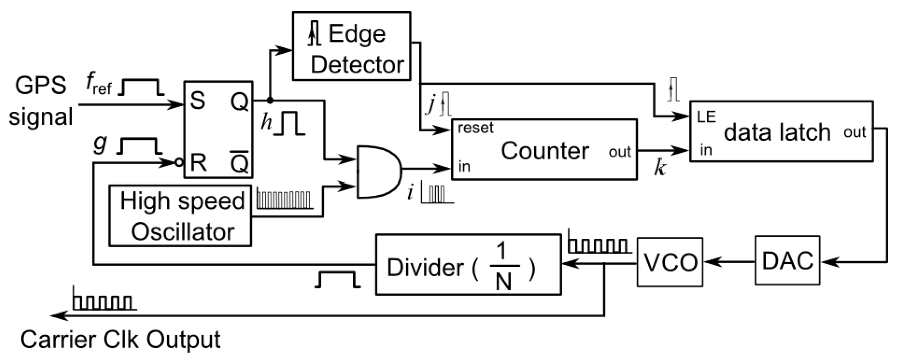
In this work, a DPLL is used to multiply the 1 Hz frequency reference and overcome the stabilization problem. A block diagram for the proposed DPLL is shown in Figure 3. A positive-edge-triggered phase comparator is used to compare the 1PPS signal with the adjusted VCO output signal (g). The phase comparator (RS Flip-Flop) output pulse width (h) represents the phase between the GPS reference signal and the adjusted VCO output pulse. Then, the comparator output is converted to a stream of high-frequency pulses (i) by gating a high-speed oscillator output with an AND gate. This pulse stream is converted to digital counts (k) using a digital counter. An edge detector is used to generate a pulse (j) that latches the digital count each cycle. Then, the latched digital count is converted to analog voltage by using a digital-to-analog converter (DAC). The DAC output is used to control the VCO output frequency. The analog voltage level will change depending on the pulse-width of counter output. In this work, the VCO is designed to generate the required output frequency at voltage level equivalent to 180-degree phase shift. Since the counter output is inverted (R = ), the signal output will be in phase with the GPS reference.
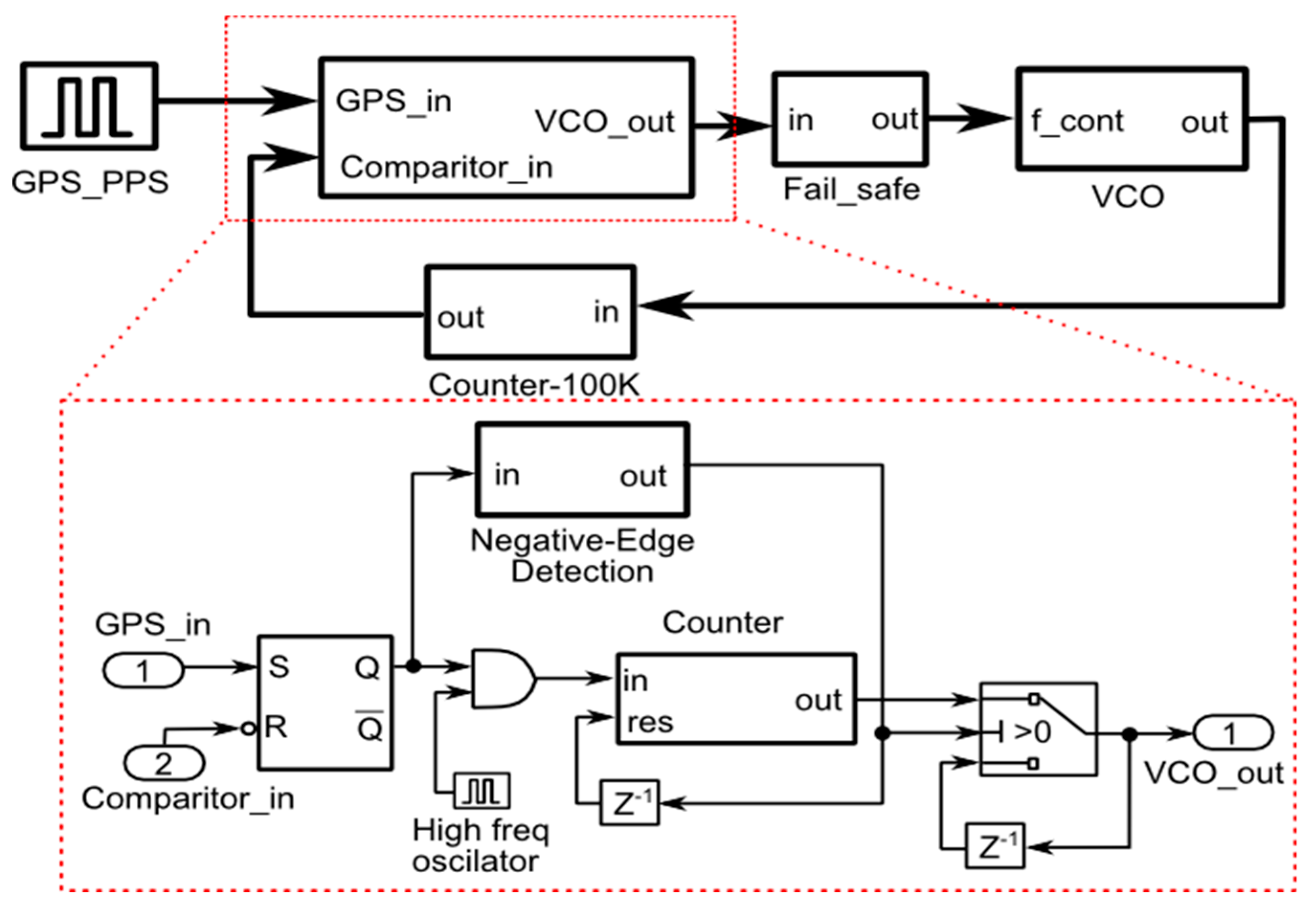
To test the performance of the proposed DPLL-based frequency multiplier, a simulation model is built within Matlab/Simulink program (Matlab 2017, Mathworks, Natick, MA, USA). The block diagram for the simulation model is shown in Figure 4. The following is a case study to test the synchronization technique using DPLL.
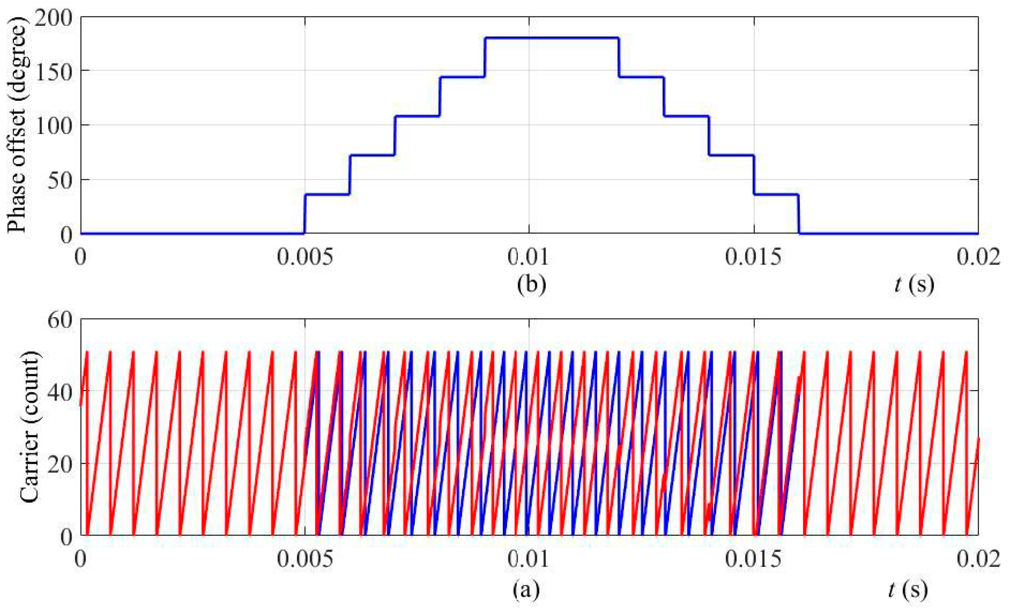
Firstly, the frequency divider output frequency was lower than GPS reference with a large phase-difference, as shown in Figure 5b. Due to the existence of the large phase shift, the VCO voltage increases and leads to higher output frequency, as shown in Figure 5c. As a result of increasing the VCO frequency, the phase shift starts to decrease between generated signal and the GPS reference signal. After 5 cycles of the GPS signals, the generated signal is locked with the GPS reference signal having the same frequency and phase-angle, as shown in Figure 5a,b. Figure 5c shows the 100 kHz frequency generated by the VCO. This high-frequency output will be used as a synchronized clock for the carrier generation module.
2.2. Carrier Generation
After generating a train of pulses with the required carrier frequency, for instance, a synchronized saw-tooth carrier must be generated. The carrier generation module will receive three input signals. These are the carrier clock, the GPS signal, and an adjustable offset. The adjustable offset is used to adjust the phase-shift between the different converter carriers. More discussion about the offset setting will be presented in Section 2.3. The operation of the carrier generation with the adjustable phase-shift module can be discussed as follows and clarified in Figure 6.
A digital counter is incrementing at each rising edge of the carrier clock pulses. When the counter reaches the peak value, a logic signal will reset the counter to zero. To ensure the saw-tooth signal is synchronized with the edge of the 1PPS GPS reference, the counter initial value will be set at the positive edge of the 1PPS signal. The generated saw-tooth signal phase is adjusted through the offset input. Each time the user adjusts the phase angle, the difference between current offset and previous offset is calculated and added to the counter. To maintain a fixed phase-shift, the offset value is loaded as an initial value at the positive edge of the 1PPS signal. A simulation model is implemented within Matlab/Simulink to test the carrier generation module.
To demonstrate the proper operation of the carrier generation model, an example for the carrier generation using different offset values is discussed. Assume two carrier generation modules working with different offset values as shown in the simulation block diagram in Figure 7. The first module “carrier 1” is supplied by zero offset, which means its carrier will be in phase with the 1PPS signal. The second module “carrier 2” is assumed to be supplied from a variable offset, which is varying from 0 to 180 degrees.
The corresponding simulation results are captured in Figure 8. The phase offset for “carrier 2” is shown in Figure 8a, and the phase angle for both carrier modules are shown in Figure 8b. The simulation starts with zero phase-angle between the two carriers. At the instant of 0.005 s, the phase offset starts incrementing from zero to 180 degrees in 0.01 s. As depicted from Figure 8b, the second carrier phase-angle follows the phase offset input and shifted with respect to “carrier 1”. When the phase offset is set back to zero at 0.015 s, the two carriers are locked in phase again. Hence, this model is accurate to synchronize between the different carriers and with the desired offset phase-shift.
2.3. Automatic Search Algorithm for Phase Offset Adjustment
Automatic Search Algorithm (ASA) is proposed to minimize DC bus ripple magnitude by adjusting the phase offset for each converter carrier. The ASA operation is inspired by Carrier-Sense Multiple Access (CSMA) communication protocol. All local controllers of DC-DC converters connected to the DC-bus will use ASA to control their local oscillator phase angles except the master converter where its phase offset will be set to zero. The ASA should increment the phase offset while monitoring the DC-bus ripple magnitude until reaching the optimal phase angle that produces a minimum ripple. Since multiple converters connected to the same DC-bus are searching for the optimal angles, it is possible for two or more converters to change their phase angles at the same time, which could disturb the operation of the control technique and lead to wrong decision. However, in the proposed technique and with the use of CSMA, this problem is mitigated.
The proposed ASA utilizes the same technique used by CSMA. It is based on detecting whether another transmission is in progress by observing the presence of carrier [26]. If a carrier is presented, the transmitter should wait for a random time before trying to initiate transmission again. In the same manner, ASA will monitor the DC-bus ripple magnitude before initiating phase control algorithm. If a change in the ripple magnitude is detected, the ASA will set a flag (new flag) to indicate detection of another converter and wait a random time before trying to modify the phase angle. To avoid the impact of noise and load change on the carrier magnitude, the ASA will ignore magnitude changes less than a predefined threshold. If there is no activity is detected, ASA will start its searching operation for the optimum angle using Perturb and Observe Technique (POT).
The ASA will increment the phase angle by a small step and observe the effect on the ripple magnitude. If the ripple is reduced the ASA will continue incrementing the phase angle until the ripple starts to increase again. POT will oscillate around the optimum phase angle. To stop oscillation, the ASA will monitor the oscillation in the phase angle and terminate POT when oscillation is detected. The ASA will allow the perturbation in one direction only to prevent oscillation in the harmonic vectors. The POT can stick in local minimum phase angle and fails to reach the global angle optimum. To avoid stuck in local minimum, the initial perturbation should be greater than or equal 2π/n, where n is the number of connected converters. In this work, ASA will adjust the increment step to π when the new flag is set and then change it to the regular increment step. The state-machine chart for the ASA operation and mechanism are shown in Figure 9.
3. Simulation Results
In this section, the DC power network shown in Figure 10 is built based on Matlab/Simulink to test and validate the robustness of the proposed approach as described in Section 2. Three DC voltage control sources are selected to represent three DGs in the DC microgrid. These sources are interfaced to the DC-bus through distributed DC-DC bidirectional converters. The converter parameters and the different DG models are listed in Table 1. The local control of each DG is implemented to control the converter duty ratio and generate its PWM carriers. All voltage and current controllers are identical to the controllers used with the GPS synchronization algorithm. The compensators are designed based on the Small Signal Model (SSM) using frequency response techniques. The derivations of SSM and control design are discussed and analyzed in detail in [27,28].
Two cases are simulated to validate the proposed approach under different operating conditions. The first case is for equal sharing load. In this case, a resistive load is fed equally from the three converters. However, in the second case, the first converter supplies 50% of the load demand while the other two converters, each one supplies 25% of the load demands each. The DC bus is desired to be regulated at 40 V and supplies a load current of 10 A.
The common voltages for DC Microgrids are 48 V, 120 V, 230 V, 325 V, and 400 V [29]. However, in this study, the voltage is scaled down to 40 V according to the rating of the available converter for experimental verification. Hence, the simulation study is performed at the same voltage level for the sack of comparison.
It is worth noting that the two case studies were selected to verify the synchronization and phase angle search algorithms’ performance. The first case studied the algorithms performance under equal power sharing condition. This case is similar to the operation of conventional multiphase interleaved converter where all phases equally share the load demand. The second case study represents more general operation scenario where each converter supplies different amount of energy and works with different duty cycle. This case is more practical for converters connected to distributed resources with different capacities.
3.1. Case 1: Equal Load Sharing
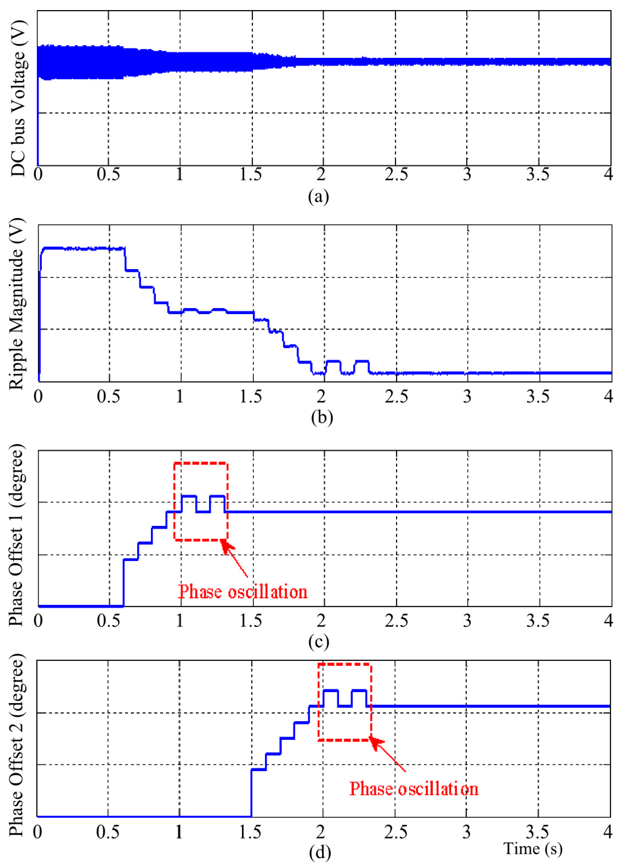
Figure 11 shows the DC bus voltage, the ripple magnitude, converter 2 phase offset, and converter 3 phase offset. Initially, all converters start with a zero-phase angle for the carriers until t = 1.0 s. At t = 1.1 s, the ASA for converter 2 starts to search for the optimum phase angle and reaches 180 degrees. At this point, the ASA detects a phase oscillation and terminates the search. During this period, the ASA for converter 3 is sensing an amplitude change in the voltage ripple and thus remains idle. After the DC voltage ripple amplitude reaches its constant state, the ASA for converter 3 starts to search for the optimal phase angle at t = 2 s. The ASA for converter 3 stops searching when the algorithm reverses the perturbing direction to prevent oscillation in the harmonic vector and reaches a phase angle equal to 30 degrees.
Similarly, during the second period, the ASA for converter 2 remains idle till the magnitude of the DC voltage ripple is stabilized again. After a random time period, the ASA for converter 2 repeats the same steps and stops at 240 degrees phase shift, whereas the ASA for converter 3 stops at 120 degrees. During the entire process, the ASA are commanded to terminate the search algorithm when the DC voltage ripple magnitude falls below 0.5 V. In this simulation, Figure 11b, the DC voltage ripple magnitude reached a minimum of 0.32 V. Figure 12 shows the phase angle between the different carriers during the search periods. Figure 12d shows the final PWM carriers along with their optimum phase shift angles. These carriers achieved significant reduction in the voltage ripple magnitude from 2.33 V to 0.32 V (Figure 11b).
3.2. Case 2: Unequal Load Sharing
The simulation results for case 2 are summarized in Figure 13 which shows the DC bus voltage, the ripple magnitude, converter 2 phase offset, and converter 3 phase offset. Initially, all converters start with a zero-phase angle for the carriers. At t = 0.6 s, the ASA for converter 2 starts to search for the optimum phase angle and reaches 180 degrees. At this point, the ASA detects a phase oscillation and terminates the search. During this period, the ASA for converter 3 is sensing an amplitude change in the voltage ripple and thus remains idle. After the DC voltage ripple amplitude reaches its steady state, the ASA for converter 3 starts to search for the optimal phase angle at t = 1.5 s. The ASA for converter 2 stops at a 240 degrees phase shift. During the entire process, the ASA are commanded to terminate the search algorithm when the DC voltage ripple falls below 0.5 V. In this case study, the DC voltage ripple reached a minimum of 0.26 V. Figure 14 shows the phase angle between carriers during the period. It can be observed that the voltage ripple magnitude with the same frequency is reduced significantly from 2.33 V to 0.26 V.
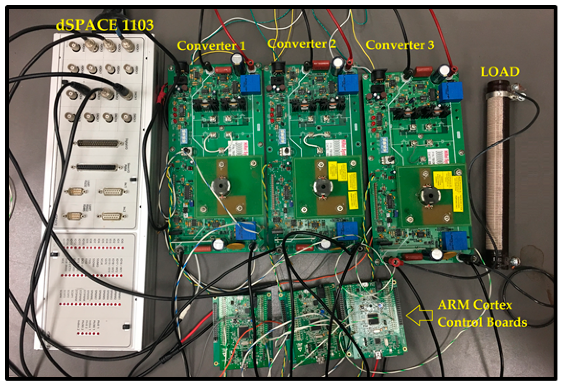
4. Hardware and Experimental Results
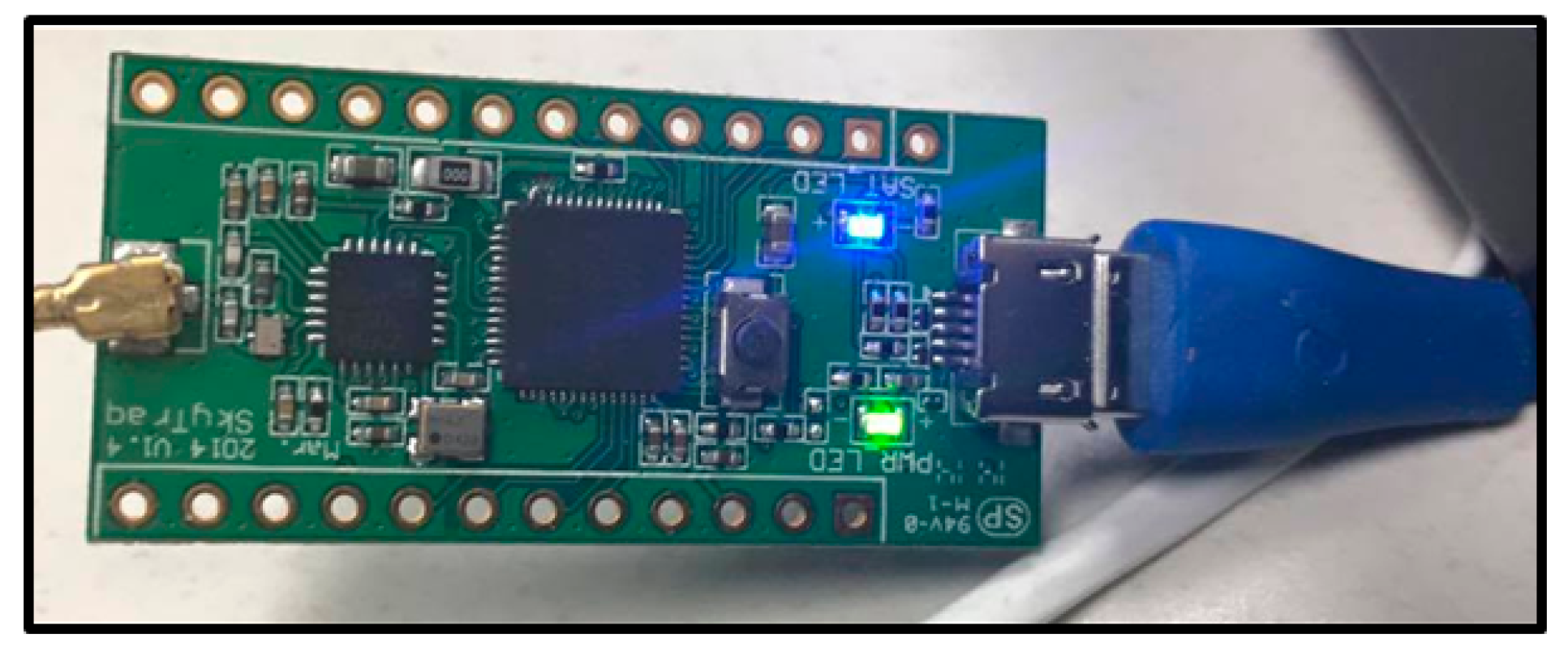
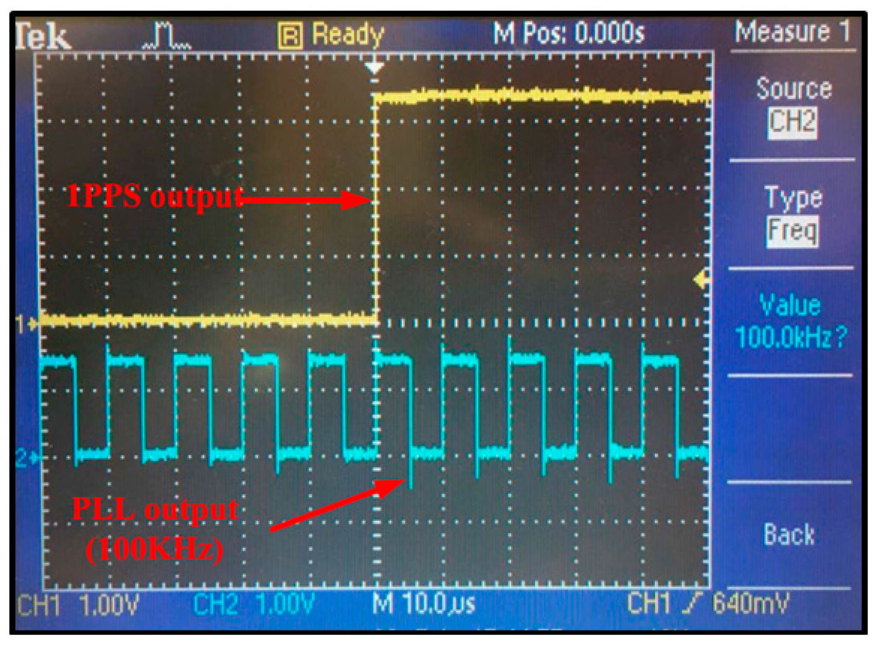
The proposed system has been implemented experimentally by developing the test bench shown in Figure 15. In this implementation, a GPS time reference module based on Venus838LPx_T GPS receiver (SkyTrak Technology, Hsinchu City 300, Taiwan) shown in Figure 16 is used [30]. The Venus838LPx_T is a single chip GPS receiver that can generate 1PPS reference time signal with 6 nanoseconds accuracy. The GPS can generate a time reference with one satellite in view. Moreover, the module has a built-in programmable PLL that produces variable frequency output ranging from 1 to 10 MHz, in this setup, the PLL is programmed to produce 100 kHz clock frequency. The output frequency is controlled using the control panel shown in Figure 17. The phase angle between the 1PPS time reference and programmed PLL output is shown in Figure 18. As depicted from this figure the module produces a high-frequency clock locked with the GPS 1PPS.
The PLL output and the 1PPS are connected to and STM32f407vgt6 ARM Cortex M4 Microcontroller (Silicon Labs, 400 West Ceser Chavez, Austin, TX, USA). The ARM microcontroller is used to implement the functions of the carrier generation and PWM. This control layer performs fast computation for the proposed algorithms and hard-real-time input/output function to control the DC-DC converters semiconductor switches. The high-speed PLL output is connected to the microcontroller interrupt input. The interrupt subroutine is executed 100 K times/s each interrupts call. The subroutine reads the offset voltage, samples the 1PPS input, and increments the counter to generate the saw-tooth carrier. For each saw-tooth cycle, the microcontroller compares the carrier with the reference received from the dSPACE 1103 (dSPACE Inc., 50131 Pontaic Trail, Wixom, MI, USA) to generate the PWM output. The STM32f407vgt6 32 Bit ARM Cortex M4 processor [31] running at 160 MHz was used for the embedded implementation of the proposed algorithm. The embedded firmware is generated from Simulink model and compiled using GNU C cross-compiler (free software) for ARM. The voltage and current control loops are implemented in dSPACE 1103 embedded controller. The duty cycle reference is transferred from dSPACE to the ARM processor as an analog reference.
The power circuit consists of three converters connected to a resistive load and 40 V common DC-bus. The controllers for the three converters are adjusted to equally share the load current as described in Case 1. The converter parameters are set the same as listed in Table 1 for the simulation results. The experimental results can be described as follows.
For the automatic search mode, assuming three converters connected in parallel, the measured DC bus voltage can be described as shown in Figure 19.
It is observed that the peak-to-peak voltage ripple is 10% from the mean output DC voltage (40 V in this case). This implies a difference between the measured and the simulation results (Figure 11a). This can be attributed to the performance of switching devices, measurement circuits, and the internal resistance of the circuit elements in the actual plant which are not ideal as considered in the simulation. Another important note is the required period to reach the steady state (which means the minimum ripple state). In the experimental test-setup, this time is a function of the digital controller sampling time which is different to the simulation sampling time. This is expected as a result of the difference in the search time to reach the optimum carrier angle for the minimum ripples. In the experimental results, the ASA reduces the voltage ripple magnitude from 4 V to 0.47 V after 5.5 s using the PWM carriers shown in Figure 19.
5. Conclusions
In this paper, a new study for distributed DG converters based on GPS synchronized carrier is presented for DC bus ripple reduction. An automatic search algorithm-based Carrier-Sense Multiple Access is implemented to minimize the DC bus voltage ripple magnitude. A DC microgrid model encompassing three DGs with their DC-DC converters is used as a prototype to test the proposed synchronization method and DC-bus ripple minimization algorithm based on Matlab/Simulink. The simulation results show that the proposed methods can generate adapted PWM carriers for Microgrid converters and reduce the DC-bus voltage ripple by more than 75%. In addition, a small power scale experimental test-bed has been built to test the proposed methods and validate the simulation results. Experimental results confirm that the proposed algorithm has successfully set an appropriate phase-shift for each converter carrier. Experimental results and the simulation results are in close agreement and matching each other in reducing the DC bus ripples.
Acknowledgments
Aboubakr Salem and Mohammad Ali Yousef Abido would like to acknowledge the support provided by the Center of Energy and Geo-Processing (CeGP), King Fahd University of Petrol & Minerals through the funded project # GTEC1701.
Author Contributions
Tarek A. Yousef gave the main idea and performed the simulation and experiments; Aboubakr Salem assisted in the simulation work and GPS synchronization model; Moataz Elsied performed the converter modelling along with and its controller; Osama A. Mohammed, Augustin Mpanda Mabwe and Mohamed Ali Yousef Abido supervised all tasks. All authors contributed to the paper writing.
Conflicts of Interest
The authors declare no conflict of interest.
Abbreviations
The following abbreviations are used in this manuscript:
| DGs | Distributed generators |
| DC | Direct Current |
| MG | Microgrid |
| DCMG | DC Microgrid |
| DAB | Dual-Active-Bridge |
| PWM | Pulse-Width Modulation. |
| EVs | Electric Vehicles |
| GPS | global positioning system |
| PLL | Phase-locked loop |
| DPLL | Digital Phase-locked loop |
| VCO | Voltage Control Oscillator |
| DAC | Digital to Analog Converter |
| 1PPS | One Pulse Per Second |
| ASA | Automatic Search Algorithm |
| CSMA | Carrier-Sense Multiple Access |
| POT | Perturb and Observe Technique |
| SSM | Small Signal Model |
Nomenclature
| Vin | Input voltage (volt) |
| Vout | Output voltage (volt) |
| L | Inductance (H) |
| fref | Reference frequency (Hz) |
| M | Number of phases of interleaved converter (phases) |
| N | Number of counts in PLL (counts) |
| R1 | Inductor resistance (Ω) |
| Rc | Capacitor internal resistance (Ω) |
| fs | Switching Frequency (Hz) |
| Cn | Capacitance (Farad) |
References
- Huang, J. A review on distributed energy resources and MicroGrid. Renew. Sustain. Energy Rev. 2008, 12, 2472–2483. [Google Scholar]
- Najy, W.K.A.; Zeineldin, H.H.; Woon, W.L. Optimal Protection Coordination for Microgrids with Grid-Connected and Islanded Capability. IEEE Trans. Ind. Electron. 2013, 60, 1668–1677. [Google Scholar] [CrossRef]
- John Justo, J.; Mwasilu, F.; Lee, J.; Jung, J.-W. AC-microgrids versus DC-microgrids with distributed energy resources: A review. Renew. Sustain. Energy Rev. 2013, 24, 387–405. [Google Scholar] [CrossRef]
- Hatziargyriou, N.; Asano, H.; Iravani, R.; Marnay, C. Microgrids. IEEE Power Energy Mag. 2007, 5, 78–94. [Google Scholar] [CrossRef]
- Siano, P. Demand response and smart grids—A survey. Renew. Sustain. Energy Rev. 2014, 30, 461–478. [Google Scholar] [CrossRef]
- Kanchev, H.; Lu, D.; Colas, F.; Lazarov, V.; Francois, B. Energy management and operational planning of a microgrid with a PV-based active generator for smart grid applications. IEEE Trans. Ind. Electron. 2011, 58, 4583–4592. [Google Scholar] [CrossRef] [Green Version]
- Karavas, C.-S.; Arvanitis, K.G.; Kyriakarakos, G.; Piromalis, D.D.; Papadakis, G. A novel autonomous PV powered desalination system based on a DC microgrid concept incorporating short-term energy storage. Solar Energy 2018, 159, 947–961. [Google Scholar] [CrossRef]
- Yoon, C.; Kim, J.; Choi, S. Multiphase DC-DC converters using a boost-half-bridge cell for high-voltage and high-power applications. IEEE Trans. Power Electron. 2011, 26, 381–388. [Google Scholar] [CrossRef]
- Das, M.; Agarwal, V. Design and Analysis of a High Efficiency DC-DC Converter with Soft Switching Capability for Renewable Energy Applications Requiring High Voltage Gain. IEEE Trans. Ind. Electron. 2016, 63, 2936–3944. [Google Scholar] [CrossRef]
- Elsied, M.; Salem, A.; Oukaour, A.; Gualous, H.; Chaoui, H.; Youssef, T.; Belie, D.; Melkebeek, J.; Mohammed, O. Efficient power-electronic converters for electric vehicle applications. In Proceedings of the 2015 IEEE Vehicle Power and Propulsion Conference (VPPC), Montreal, QC, Canada, 19–22 October 2015. [Google Scholar]
- Zhang, K.; Shan, Z.; Jatskevich, J. Large- and Small-Signal Average-Value Modeling of Dual-Active-Bridge DC-DC Converter Considering Power Losses. IEEE Trans. Power Electron. 2017, 32, 1964–1974. [Google Scholar] [CrossRef]
- Gu, Y.; Zhang, D. Interleaved Boost Converter with Ripple Cancellation Network. IEEE Trans. Power Electron. 2013, 28, 3860–3869. [Google Scholar] [CrossRef]
- Zhou, L.; Zhu, B.; Luo, Q.; Chen, S. Interleaved non-isolated high step-up DC/DC converter based on the diode–capacitor multiplier. IET Power Electron. 2014, 7, 390–397. [Google Scholar] [CrossRef]
- Salem, A.; Elsied, M.; Druant, J.; de Belie, F.; Oukaour, A.; Gualous, H.; Melkebeek, J. An Advanced Multilevel Converter Topology with Reduced Switching Elements. In Proceedings of the 40th Annual Conference of the IEEE Industrial Electronics IECON 2014, Dallas, TX, USA, 29 October–1 November 2014. [Google Scholar]
- Thounthong, P.; Davat, B. Study of a multiphase interleaved step-up converter for fuel cell high power applications. Energy Convers. Manag. 2010, 51, 826–832. [Google Scholar] [CrossRef]
- Lai, C.-M.; Pan, C.; Cheng, M. High-efficiency modular high step-up interleaved boost converter for DC-microgrid applications. IEEE Trans. Ind. Appl. 2012, 48, 161–171. [Google Scholar] [CrossRef]
- Omara, A.M.; Sleptsov, M. Bidirectional interleaved DC/DC converter for electric vehicle application. In Proceedings of the 2016 11th International Forum on Strategic Technology (IFOST), Novosibirsk, Russia, 1–3 June 2016. [Google Scholar]
- Miwa, B.A. Interleaved Conversion Techniques for High Density Power Supplies. Ph.D. Thesis, Department of Electronic Engineering Computer Science, Massachusetts Institute of Technology, Cambridge, MA, USA, June 1992. [Google Scholar]
- Giral, R.; Martinez-Salamero, L.; Singer, S. Interleaved converters operation based on CMC. IEEE Trans. Power Electron. 1999, 14, 643–652. [Google Scholar] [CrossRef]
- Prodic, A.; Maksimovic, D.; Erickson, R.W. Design and implementation of a digital PWM controller for a high-frequency switching DC-DC power converter. In Proceedings of the 27th Annual Conference of the IEEE Industrial Electronics Society, Denver, CO, USA, 29 November–2 December 2001; Volume 2. [Google Scholar]
- Li, P. Synchronization and Control of High Frequency DC-DC Converters. Ph.D. Thesis, Florida University, Gainesville, FL, USA, 2009. [Google Scholar]
- IEEE Std. 1588–2008. IEEE Standard for a Precision Clock Synchronization Protocol for Networked Measurement and Control Systems. Available online: http://www.nist.gov/el/isd/ieee/ieee 1588 (accessed on 28 February 2016).
- National Instruments. Timing and Synchronization Systems. Available online: http://www.ni.com/ white-paper/9882/en/ (accessed on 28 February 2016).
- Ogaja, C.A. Applied GPS for Engineers and Project Managers; American Society of Civil Engineers: Reston, VA, USA, 2011. [Google Scholar]
- Global Positioning System. Available online: https://www.faa.gov/about/office.org/hea-dquartersoffices/ato/service_units/techop/navservices/gnss/faq/gps/ (accessed on 27 February 2017).
- Douglas, S.C.; Berger, T.; Tong, L. Carrier Sense Multiple Access Communications on Multipacket Reception Channels: Theory and Applications to IEEE 802.11 Wireless Networks. IEEE Trans. Commun. 2013, 61, 266–278. [Google Scholar]
- Elsied, M.; Oukaour, A.; Chaoui, H.; Gualous, H. Real-time implementation of four-phase interleaved DC-DC boost converter for electric vehicle power system. Electr. Power Syst. Res. 2016, 141, 210–220. [Google Scholar] [CrossRef]
- Ayoubi, Y.; Elsied, M.; Oukaour, A.; Chaoui, H.; Slamani, Y.; Gualous, H. Four-phase interleaved DC/DC boost converter interfaces for super-capacitors in electric vehicle application based on advanced sliding mode control design. Electr. Power Syst. Res. 2016, 134, 186–196. [Google Scholar] [CrossRef]
- Anand, S.; Fernandes, B.G. Optimal voltage level for DC microgrids. In Proceedings of the IECON 2010—36th Annual Conference on IEEE Industrial Electronics Society, Glendale, AZ, USA, 7–10 November 2010. [Google Scholar]
- Timing Mode GPS Receiver. Venus838LPx-T-L/Venus838LPx-T-D. Available online: http://navspark.mybigcommerce.com/content/Venus838LPx-T_DS_v2.pdf (accessed on 28 December 2014).
- STMicroelectronics, STM32F4 Series of High Performance MCUs with DSP and FPU Instructions. Available online: http://www2.st.com/content/stcom/en/pro ducts/microcontrollers.html (accessed on 20 December 2017).
Figure 1.
Proposed system block diagram (a) one unit of the converter system including controller; (b) DC Bus connected to n-unit converter system; (c) conventional boost converter.
Figure 1.
Proposed system block diagram (a) one unit of the converter system including controller; (b) DC Bus connected to n-unit converter system; (c) conventional boost converter.
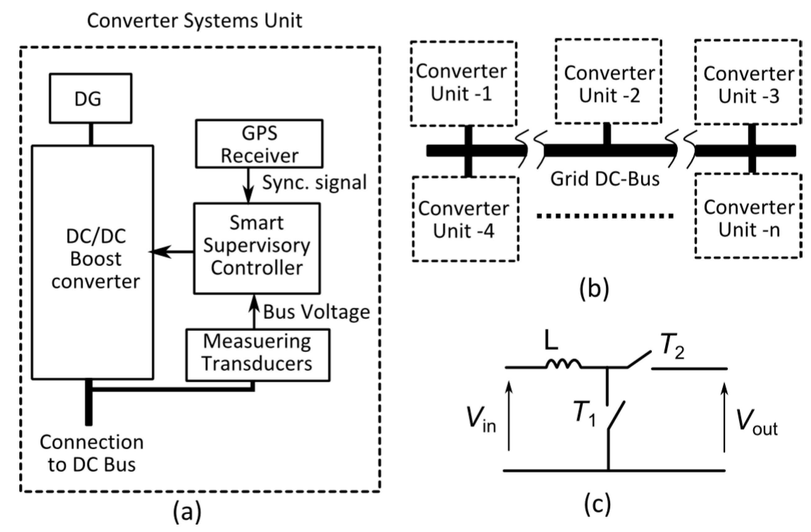
Figure 2.
Frequency multiplier using phase locked loop (PLL).
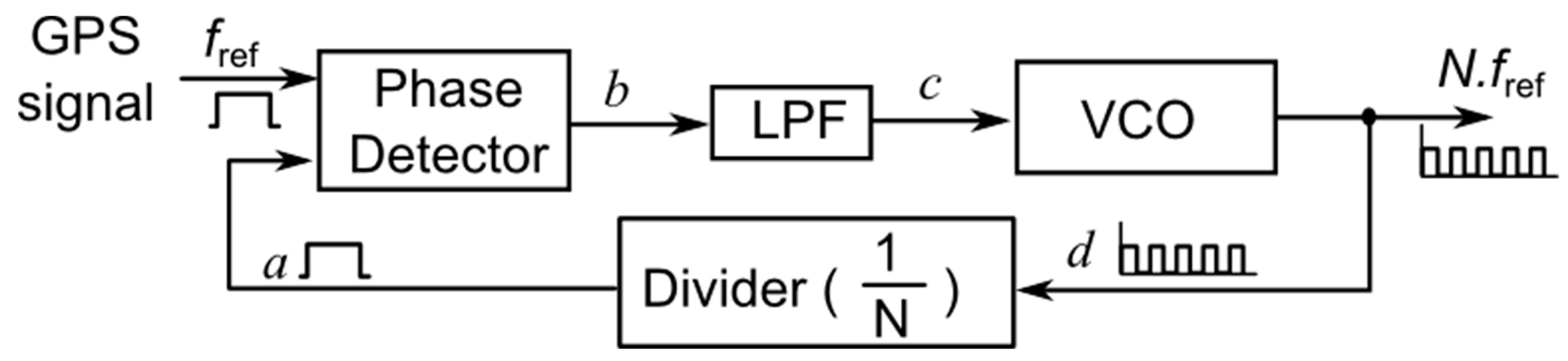
Figure 3.
Frequency multiplier using DPLL.

Figure 4.
Block diagram for the DPLL using Matlab\Simulink.

Figure 5.
Proposed DPLL simulation performance.
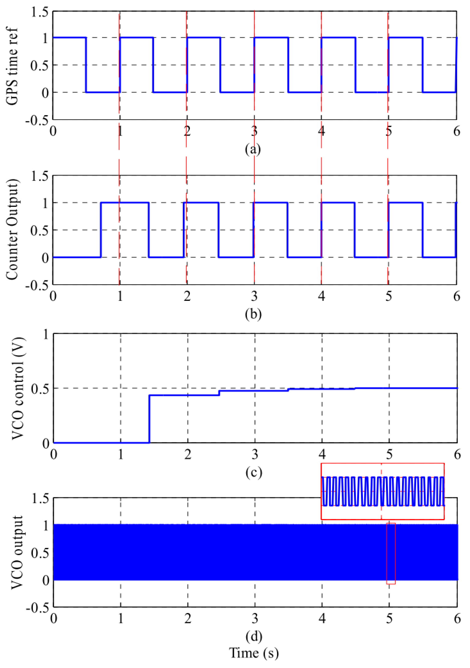
Figure 6.
Carrier generation simulation model block-diagram.
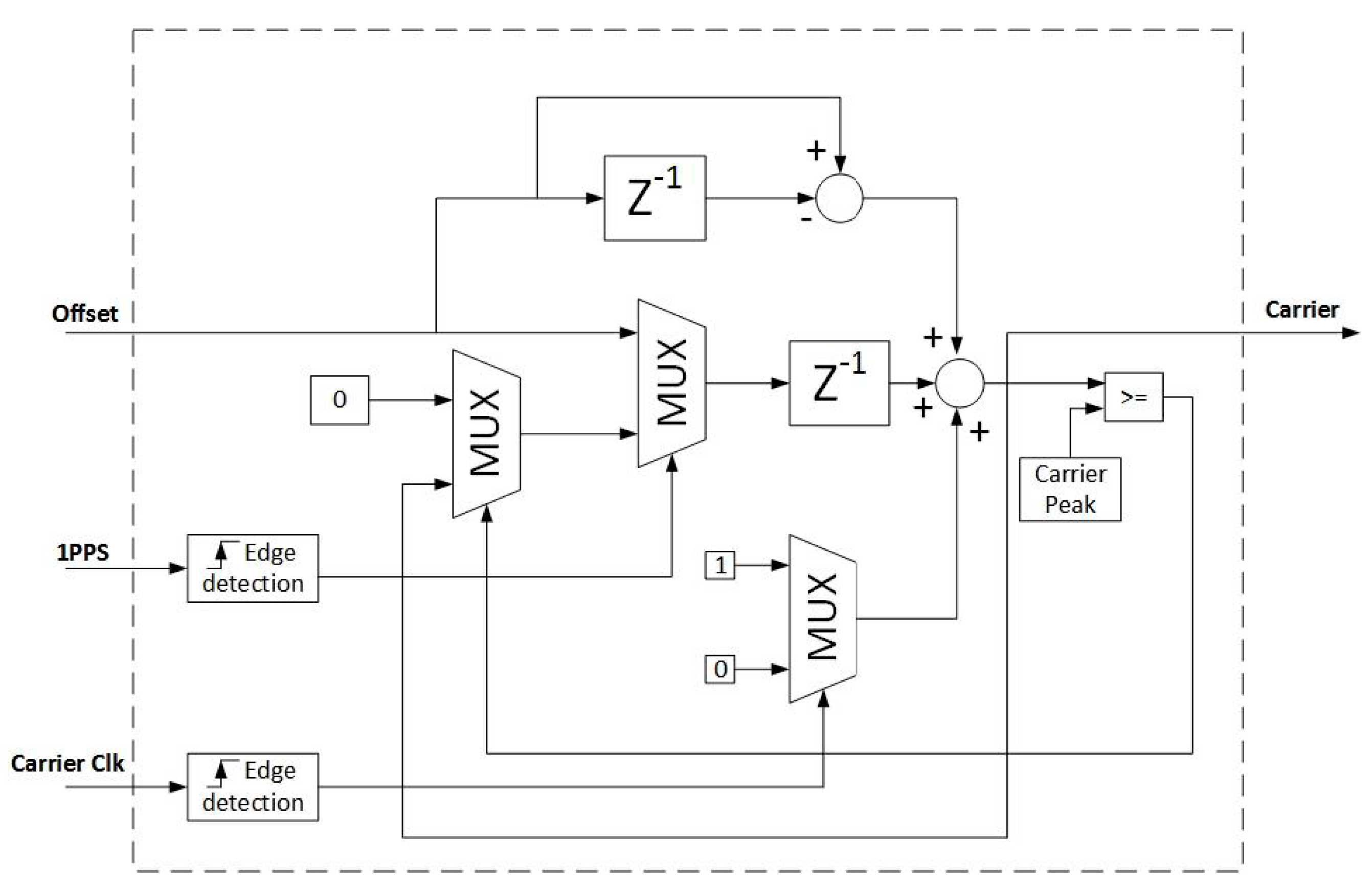
Figure 7.
Phase adjustment simulation model block-diagram.
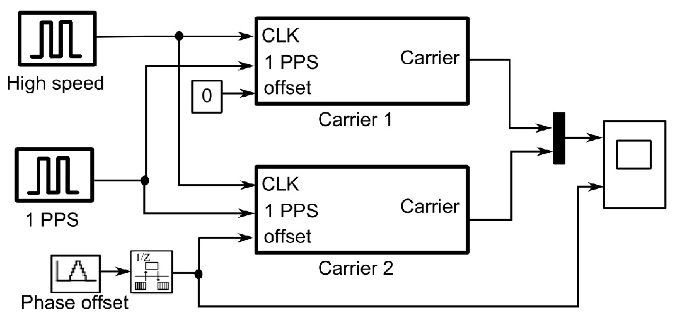
Figure 8.
Carrier phase adjustment performance (a) carrier 2 offset; (b) the two carrier signals.

Figure 9.
Automatic search algorithm state machine.
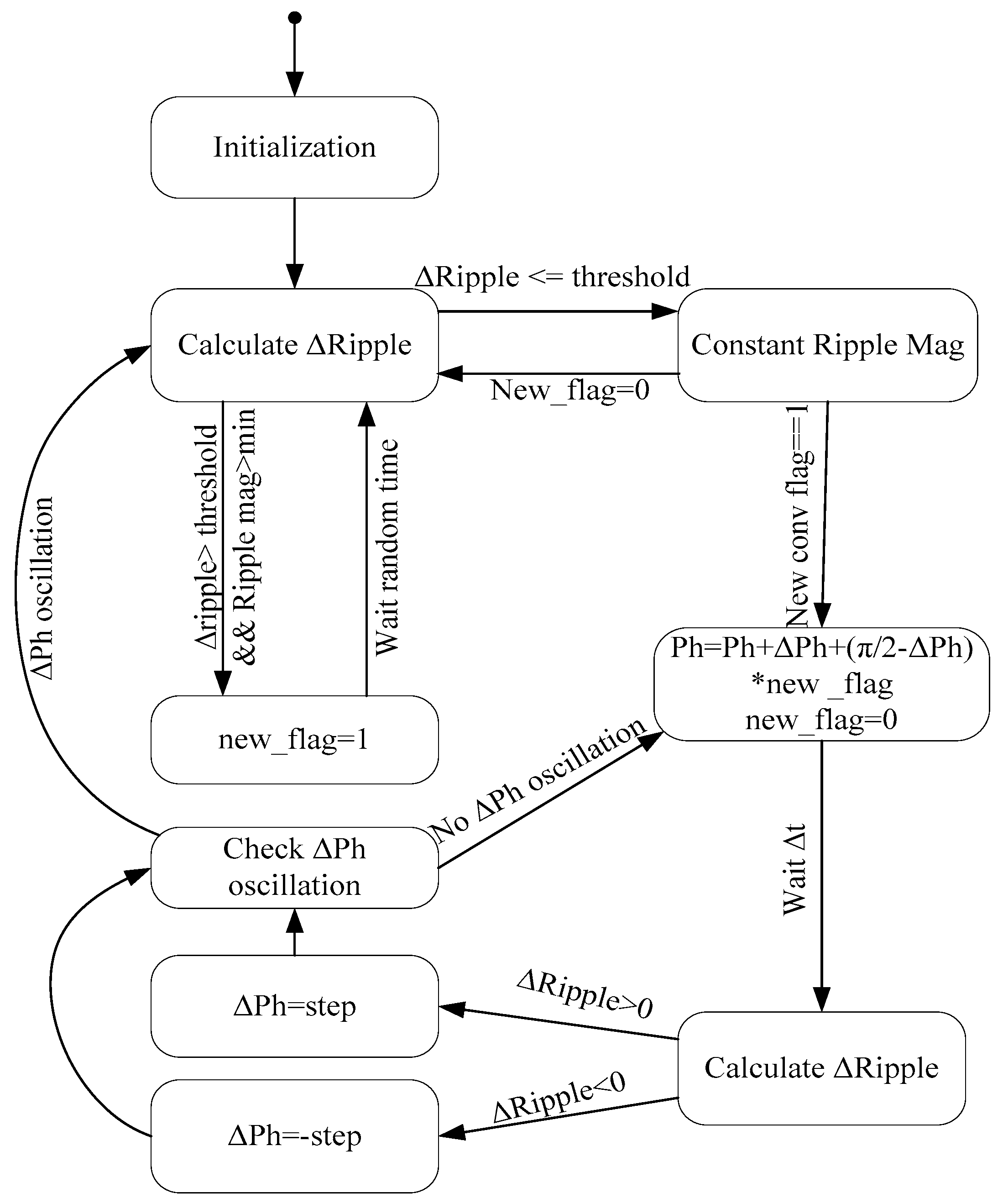
Figure 10.
DC Microgrid power network.
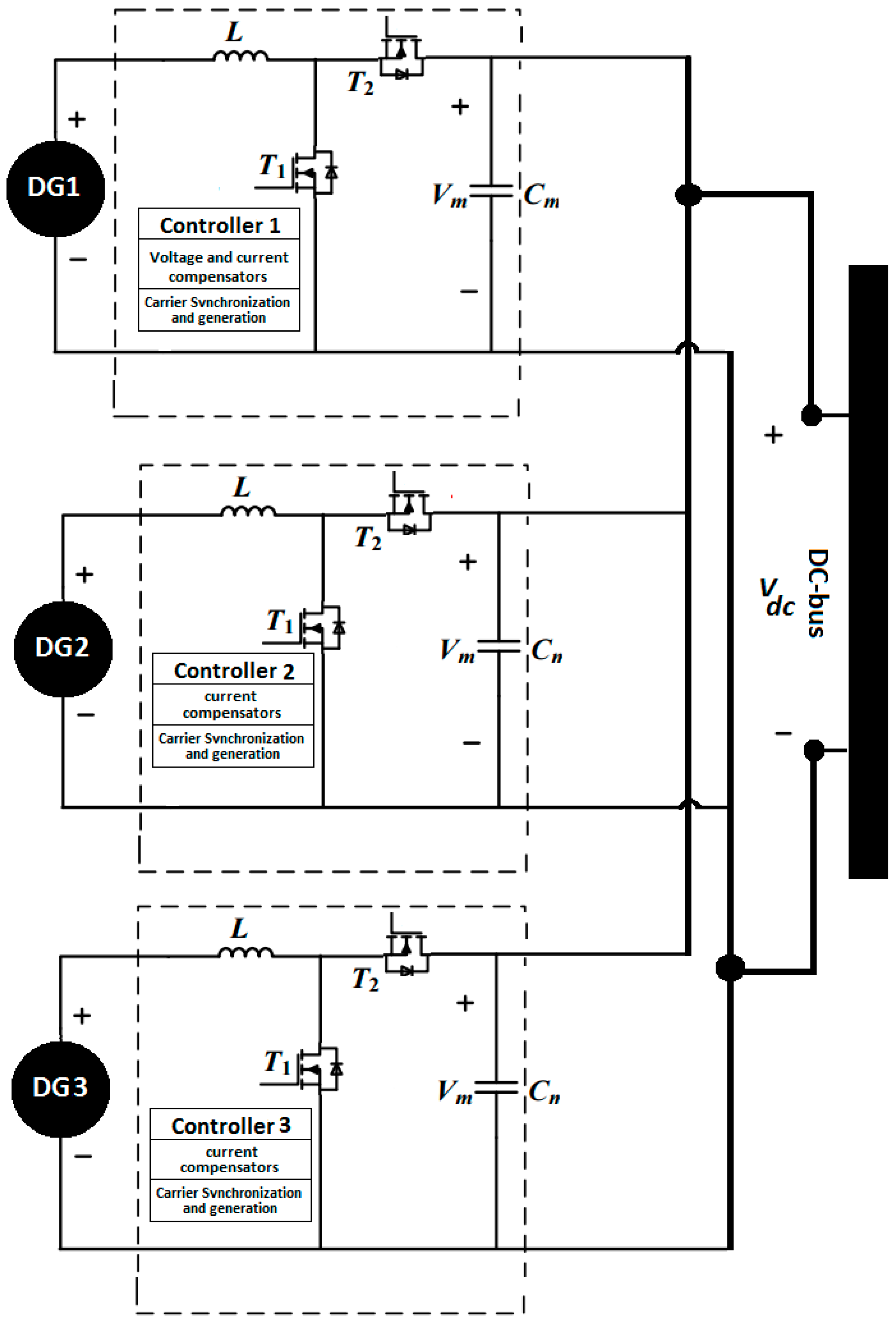
Figure 11.
Case 1 simulation results for equal load sharing (a) DC bus voltage ripple; (b) Ripple Magnitude; (c) Converter 2 phase-offset; (d) Converter 3 phase-offset.
Figure 11.
Case 1 simulation results for equal load sharing (a) DC bus voltage ripple; (b) Ripple Magnitude; (c) Converter 2 phase-offset; (d) Converter 3 phase-offset.
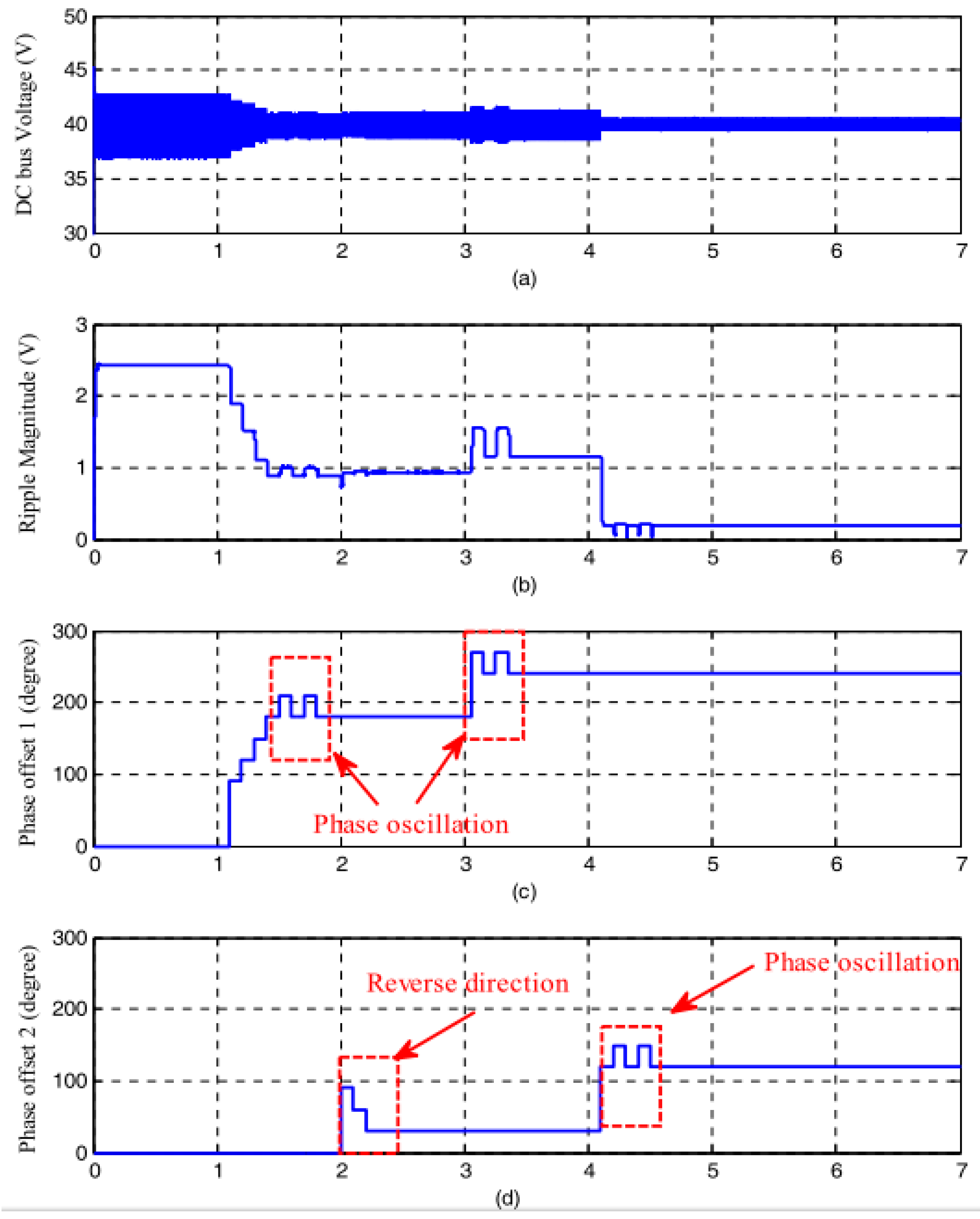
Figure 12.
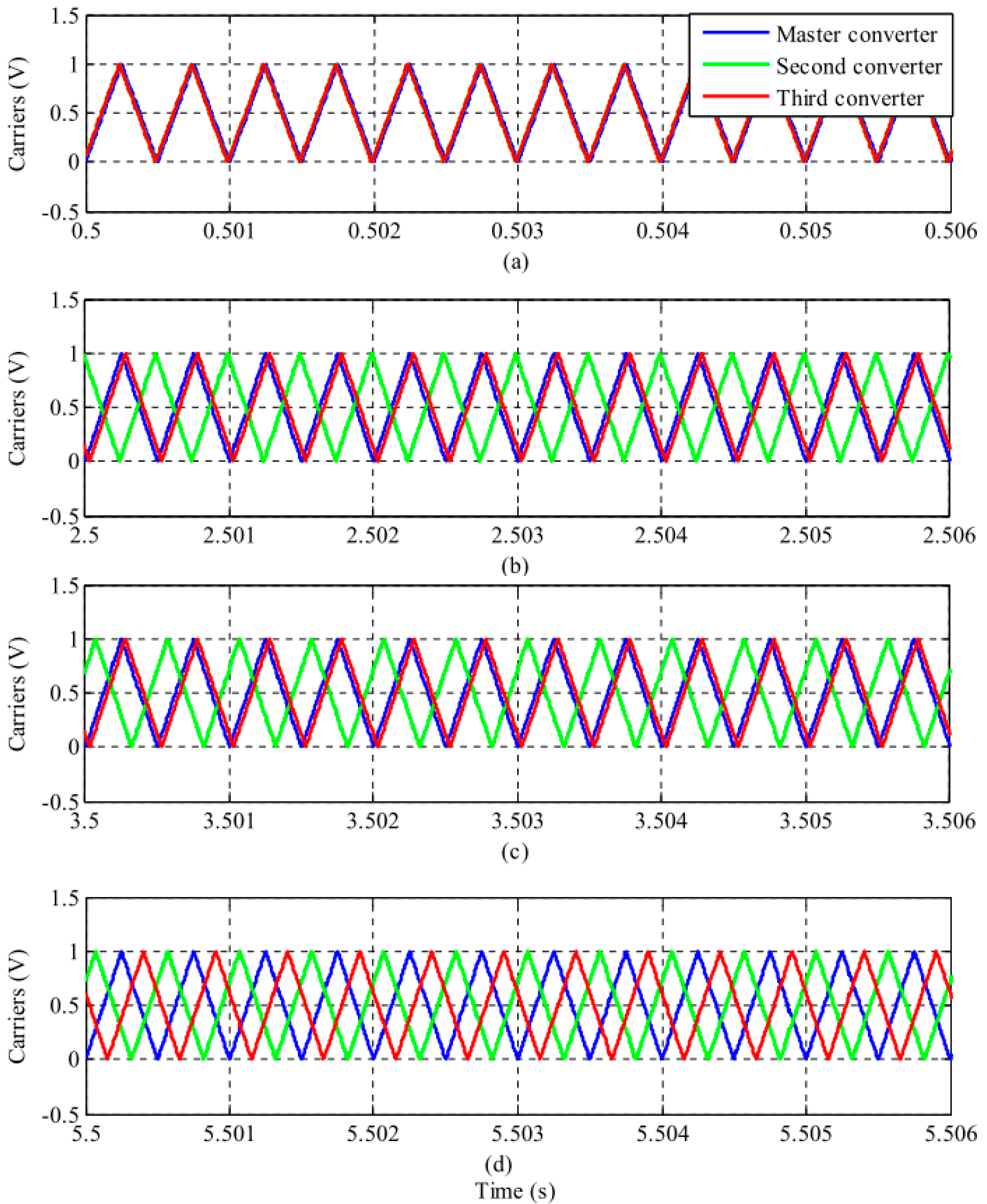
(Case 1) Carriers phase angles for case 1. (a) Carriers at t = 0 s; (b) Carriers at t = 2.5 s; (c) Carriers at t = 3.5 s; (d) Carriers at t = 5.5 s.
Figure 12.
(Case 1) Carriers phase angles for case 1. (a) Carriers at t = 0 s; (b) Carriers at t = 2.5 s; (c) Carriers at t = 3.5 s; (d) Carriers at t = 5.5 s.

Figure 13.
(Case 2) simulation results for unequal load sharing. (a) DC bus Voltage; (b) Ripple Magnitude; (c) Converter 2 phase-offset; (d) Converter 3 phase-offset.
Figure 13.
(Case 2) simulation results for unequal load sharing. (a) DC bus Voltage; (b) Ripple Magnitude; (c) Converter 2 phase-offset; (d) Converter 3 phase-offset.

Figure 14.
(Case 2) Carriers phase angles for case 2. (a) Carriers at t = 0.5 s; (b) Carriers at t = 1.5 s; (c) Carriers at t = 2.5 s.
Figure 14.
(Case 2) Carriers phase angles for case 2. (a) Carriers at t = 0.5 s; (b) Carriers at t = 1.5 s; (c) Carriers at t = 2.5 s.
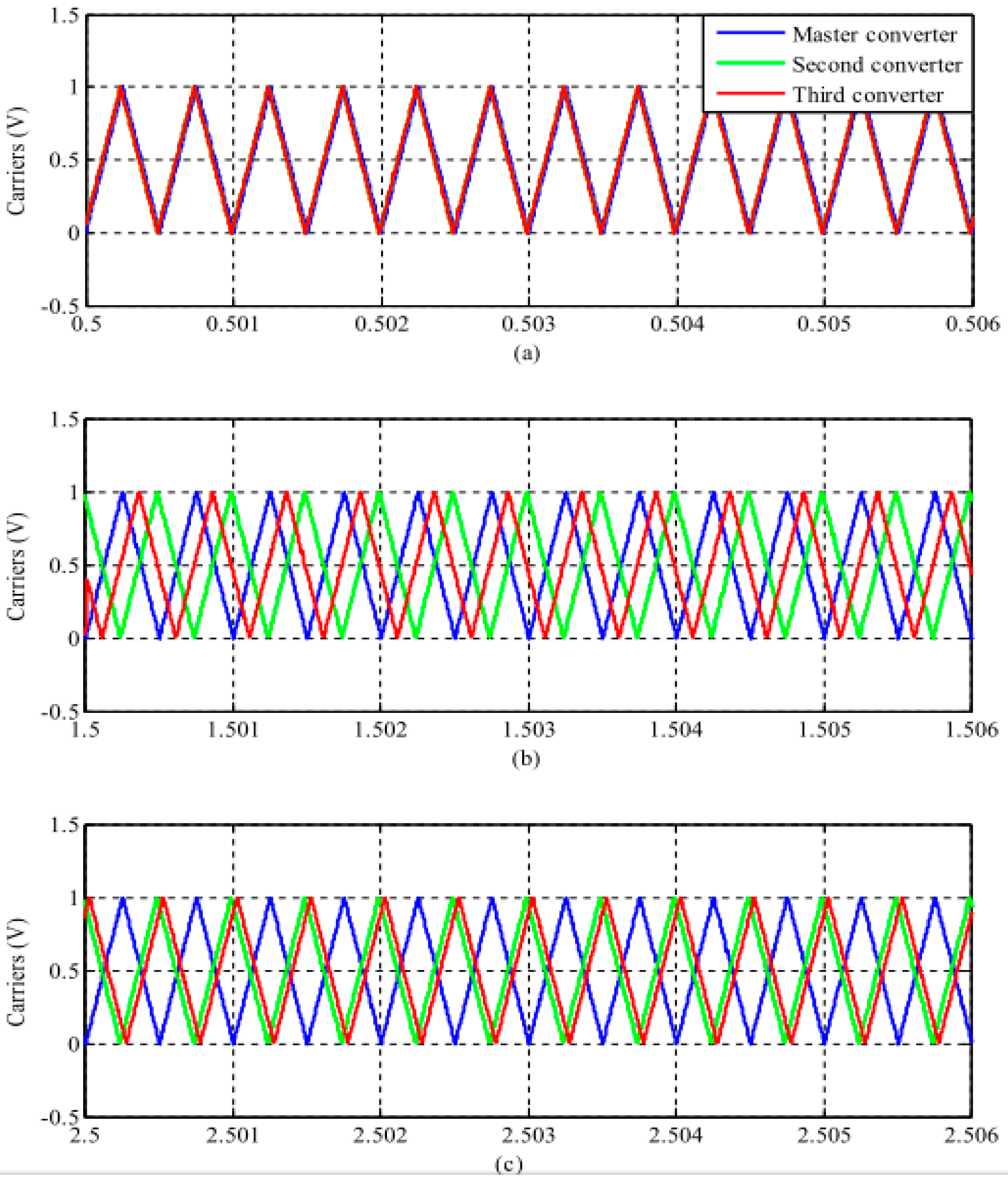
Figure 15.
Hardware setup for the GPS carrier synchronization.

Figure 16.
GPS timing Module.

Figure 17.
The GPS software control panel.
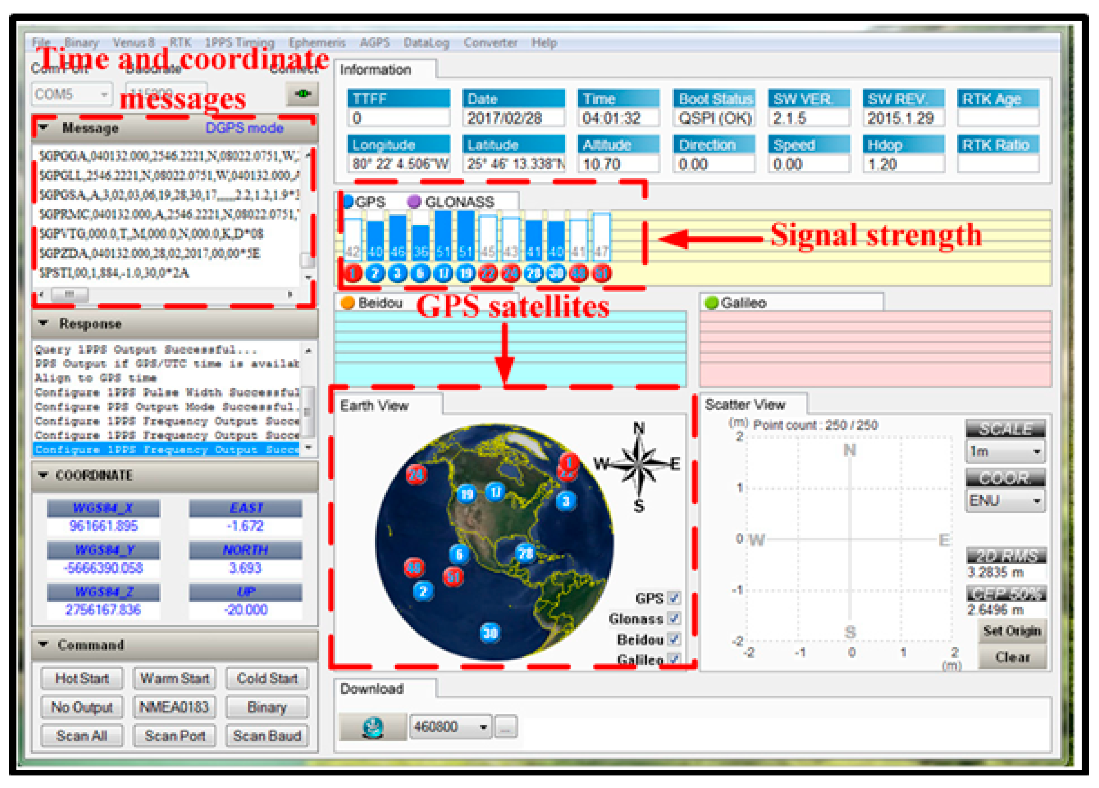
Figure 18.
1PPS and high-frequency output signal.

Figure 19.
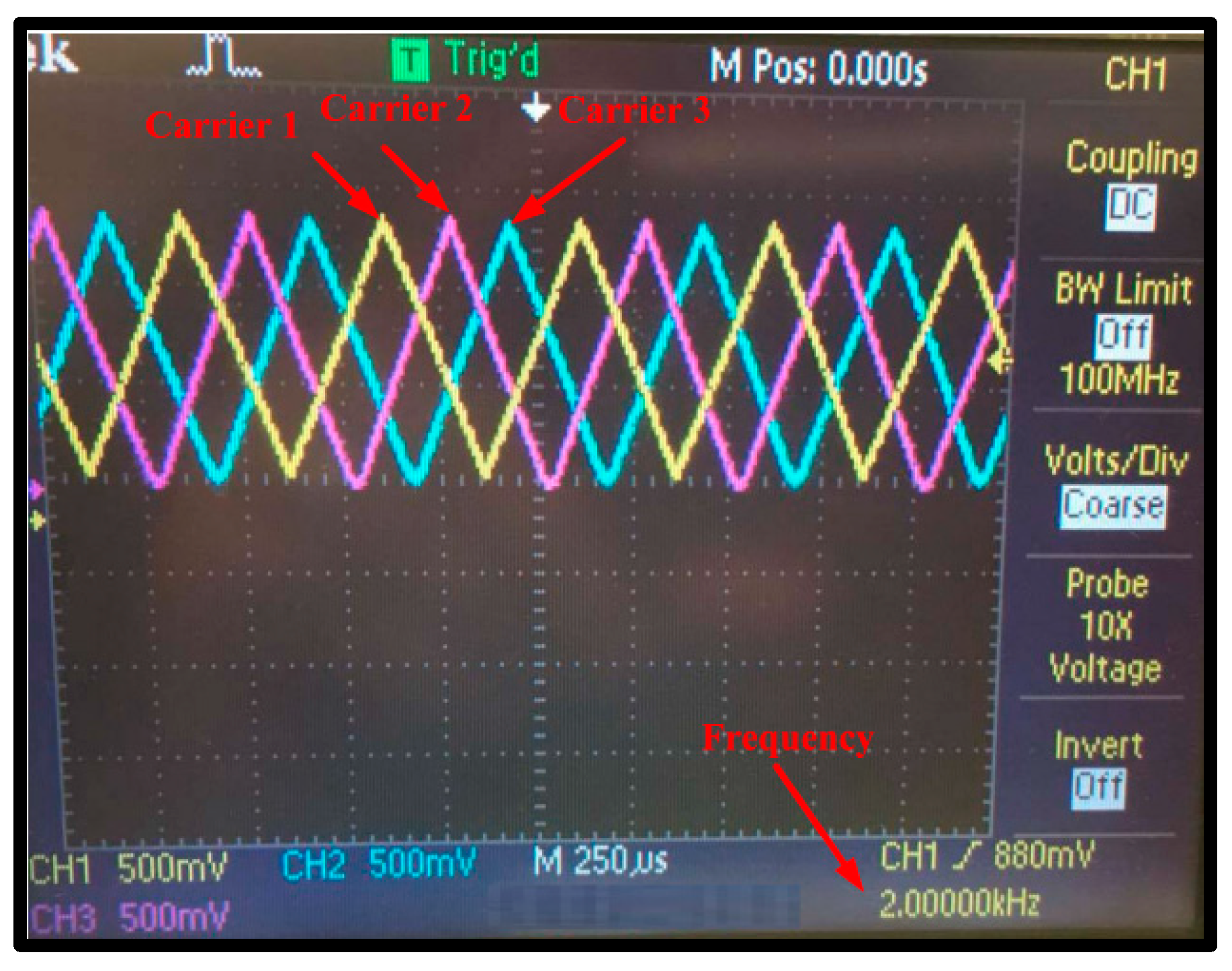
Automatic search mode DC bus voltage for three parallel converters.
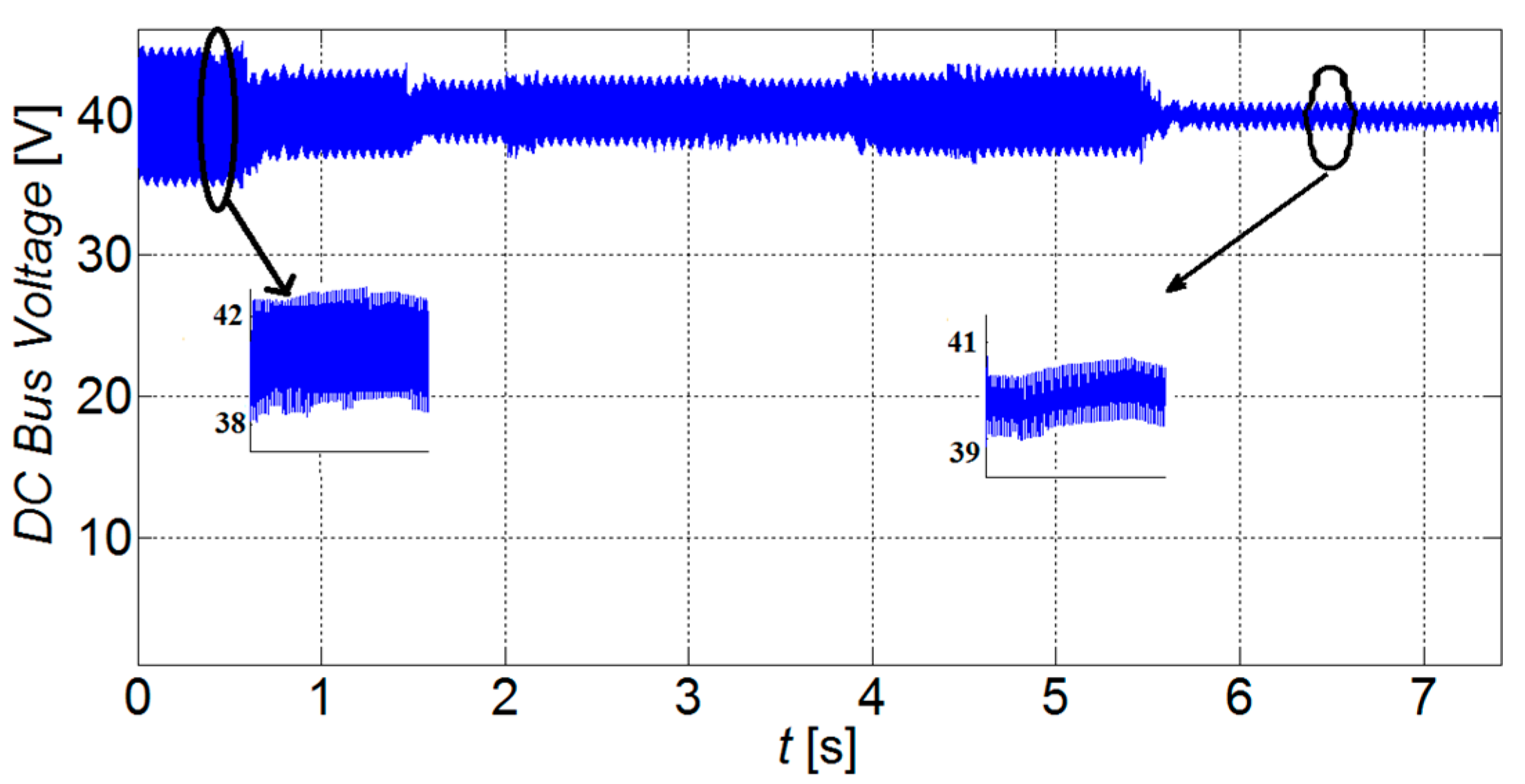
Figure 20.
Three converter carriers after ASA.

Table 1.
DC power network parameters.
| Parameters | Values |
|---|---|
| Inductance (L) | 750 µH |
| Inductor resistance () | 20 mΩ |
| Capacitance (Cn) | 312 µF |
| Capacitor Resistance ( | 0.575 mΩ |
| DC Bus voltage | 40 V |
| DG1 output voltage (Dimethyl Ether—50 stack of 0.5 V) | 25 V |
| DG2 output voltage (PV 22 V, 50 W) | 22 V |
| DG3 output voltage (Battery: Li-poly 5 cells) | 20 V |
| Load resistance | 4 Ω |
| Switching Frequency (fs) | 2 kHz |
© 2018 by the authors. Licensee MDPI, Basel, Switzerland. This article is an open access article distributed under the terms and conditions of the Creative Commons Attribution (CC BY) license (http://creativecommons.org/licenses/by/4.0/).
Share and Cite
MDPI and ACS Style
Youssef, T.A.; Salem, A.; Elsied, M.; Mabwe, A.M.; Abido, M.A.Y.; Mohammed, O.A. GPS Synchronization of Smart Distributed Converters for Microgrid Applications. Energies 2018, 11, 695. https://doi.org/10.3390/en11040695
AMA Style
Youssef TA, Salem A, Elsied M, Mabwe AM, Abido MAY, Mohammed OA. GPS Synchronization of Smart Distributed Converters for Microgrid Applications. Energies. 2018; 11(4):695. https://doi.org/10.3390/en11040695
Chicago/Turabian StyleYoussef, Tarek A., Aboubakr Salem, Moataz Elsied, Augustin Mpanda Mabwe, Mohammad Ali Yousef Abido, and Osama A. Mohammed. 2018. "GPS Synchronization of Smart Distributed Converters for Microgrid Applications" Energies 11, no. 4: 695. https://doi.org/10.3390/en11040695
Note that from the first issue of 2016, this journal uses article numbers instead of page numbers. See further details here.