Novel Cathode Design to Improve the ESD Capability of 600 V Fast Recovery Epitaxial Diodes

 , ,
, ,  ,
, 
 ,
,
Abstract
:1. Introduction
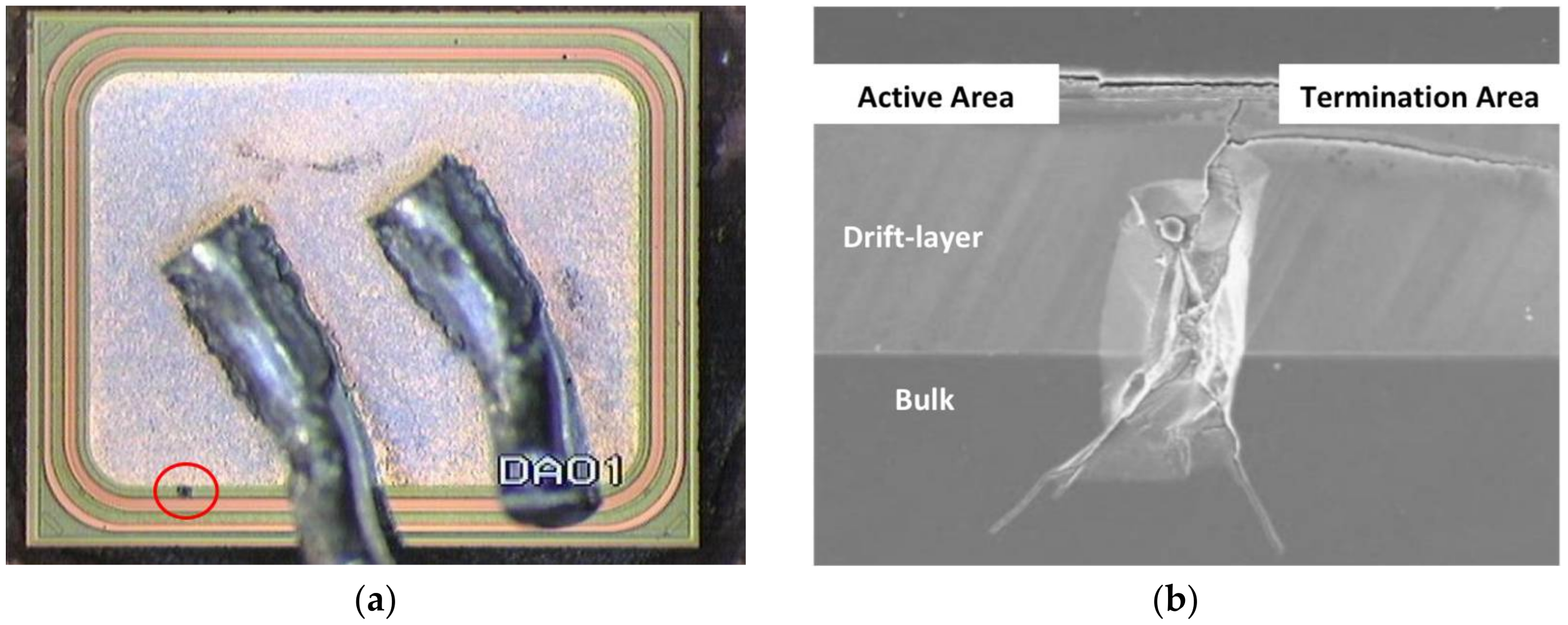
2. ESD Failures
3. Theoretical Background
4. Numerical Results
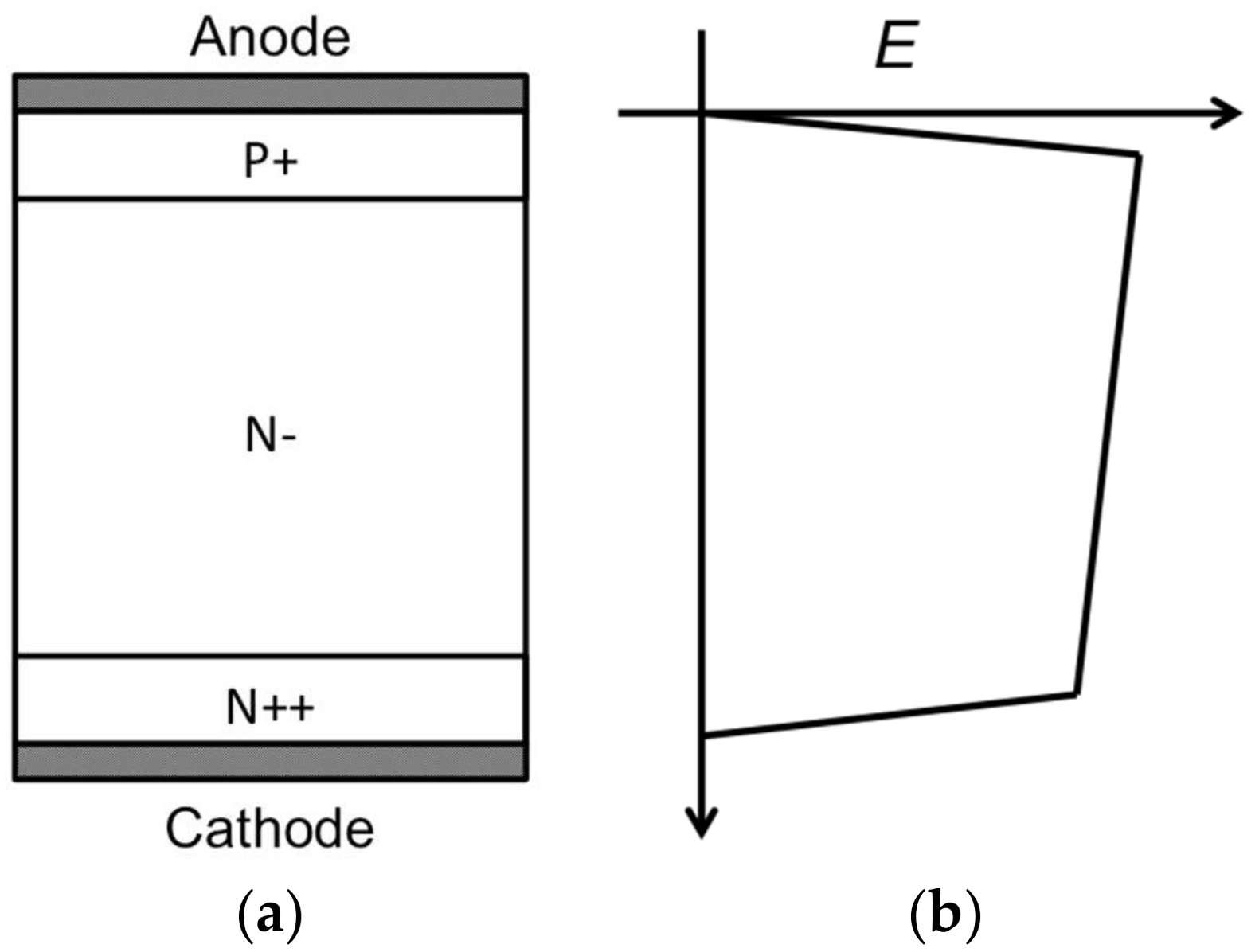
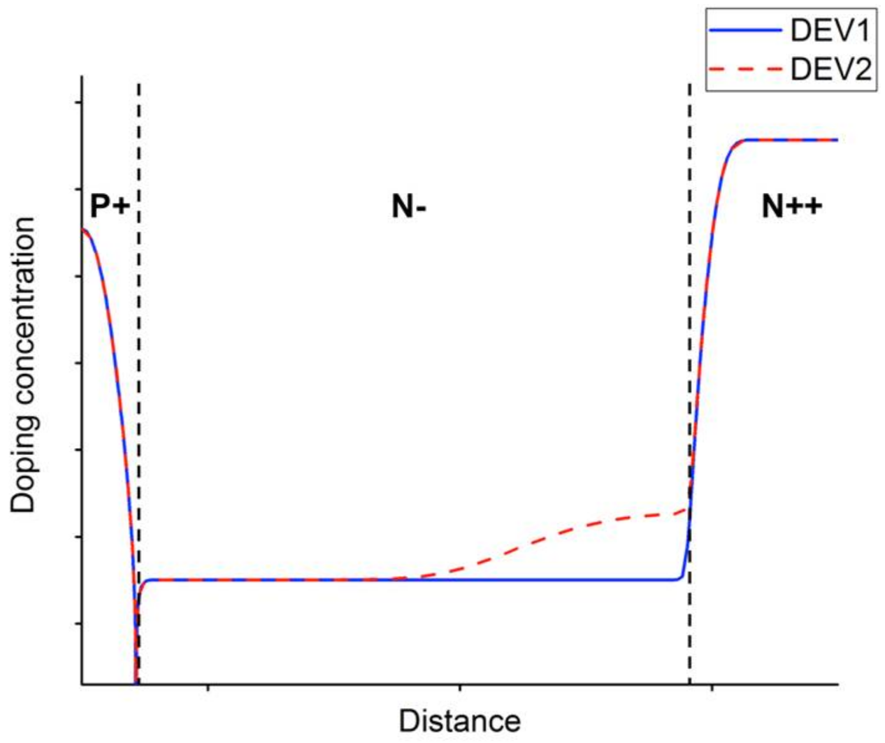
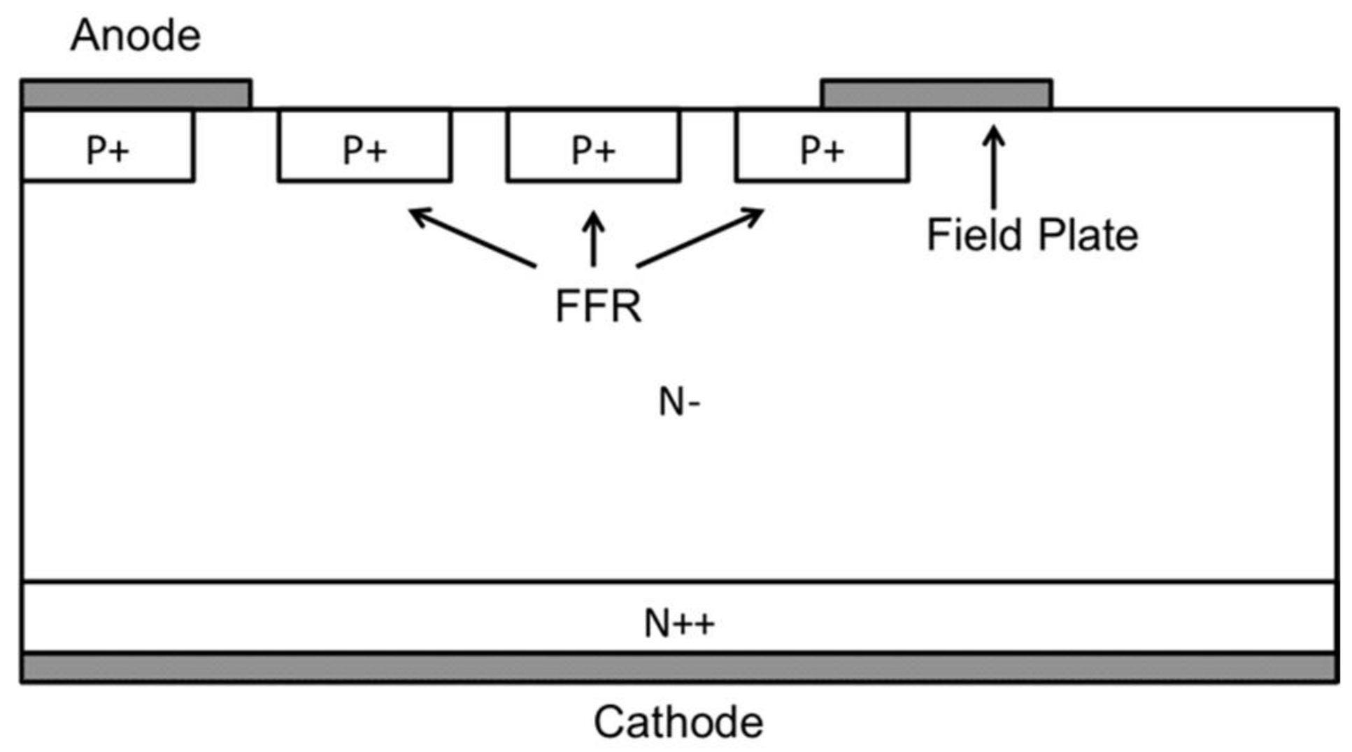
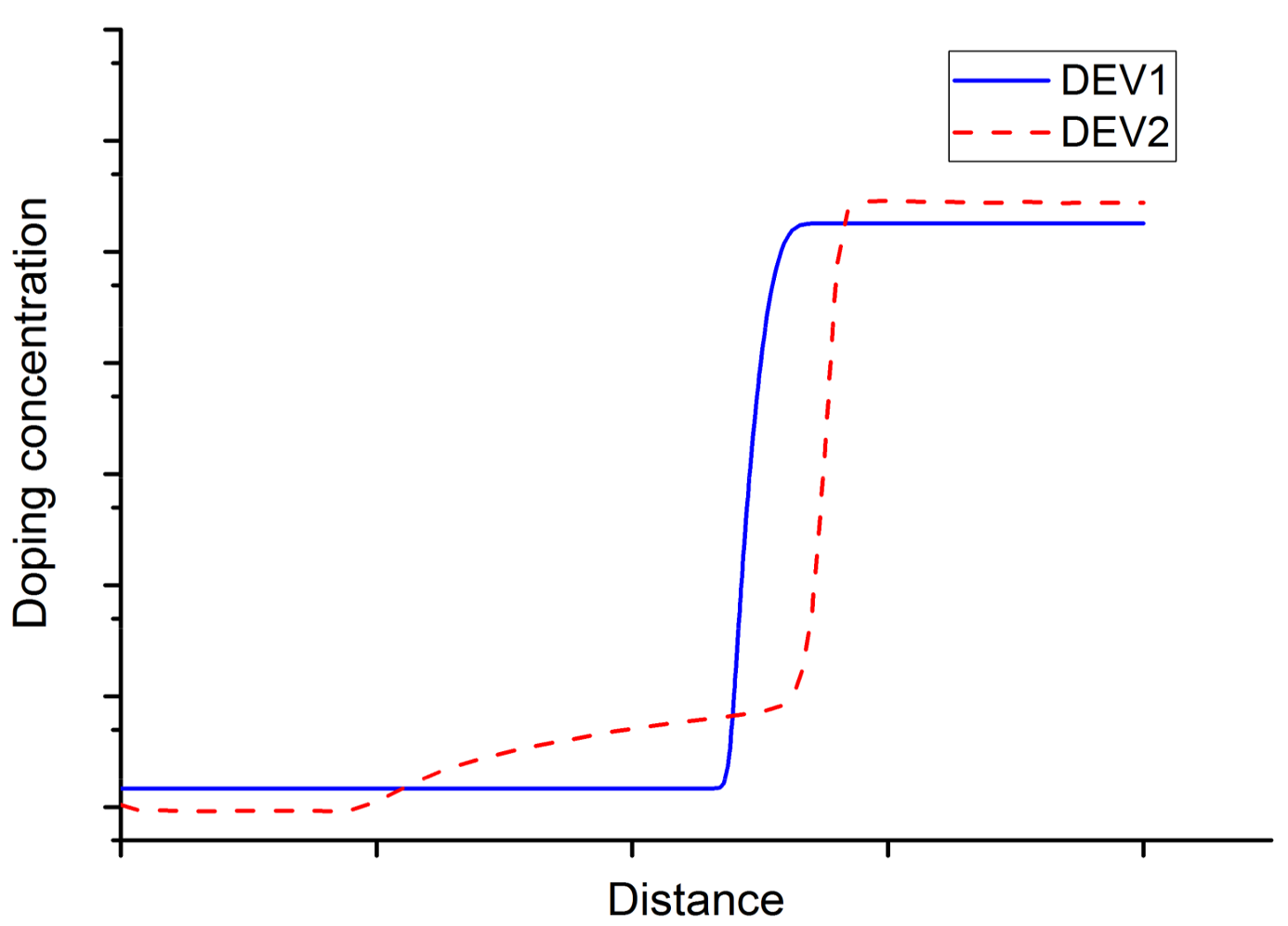
4.1. Doping Profiles
4.2. Elementary Cell Analysis
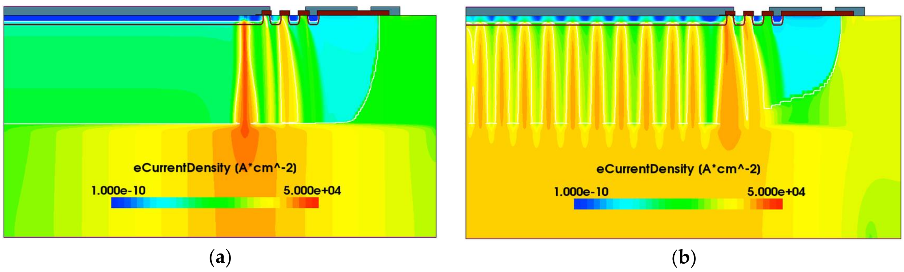
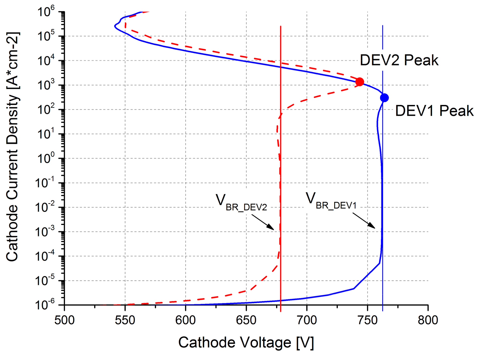
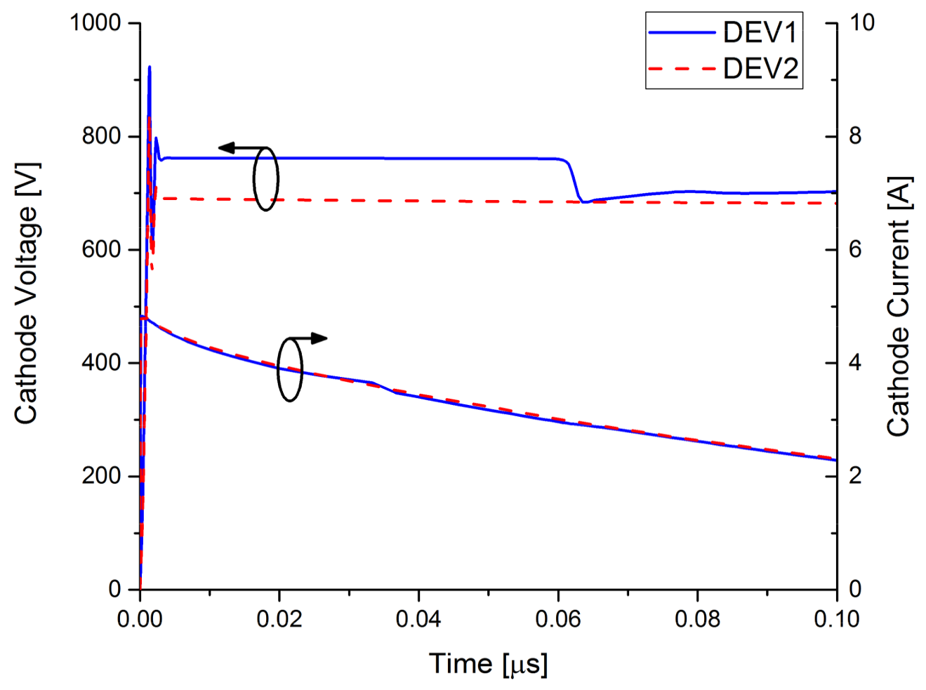
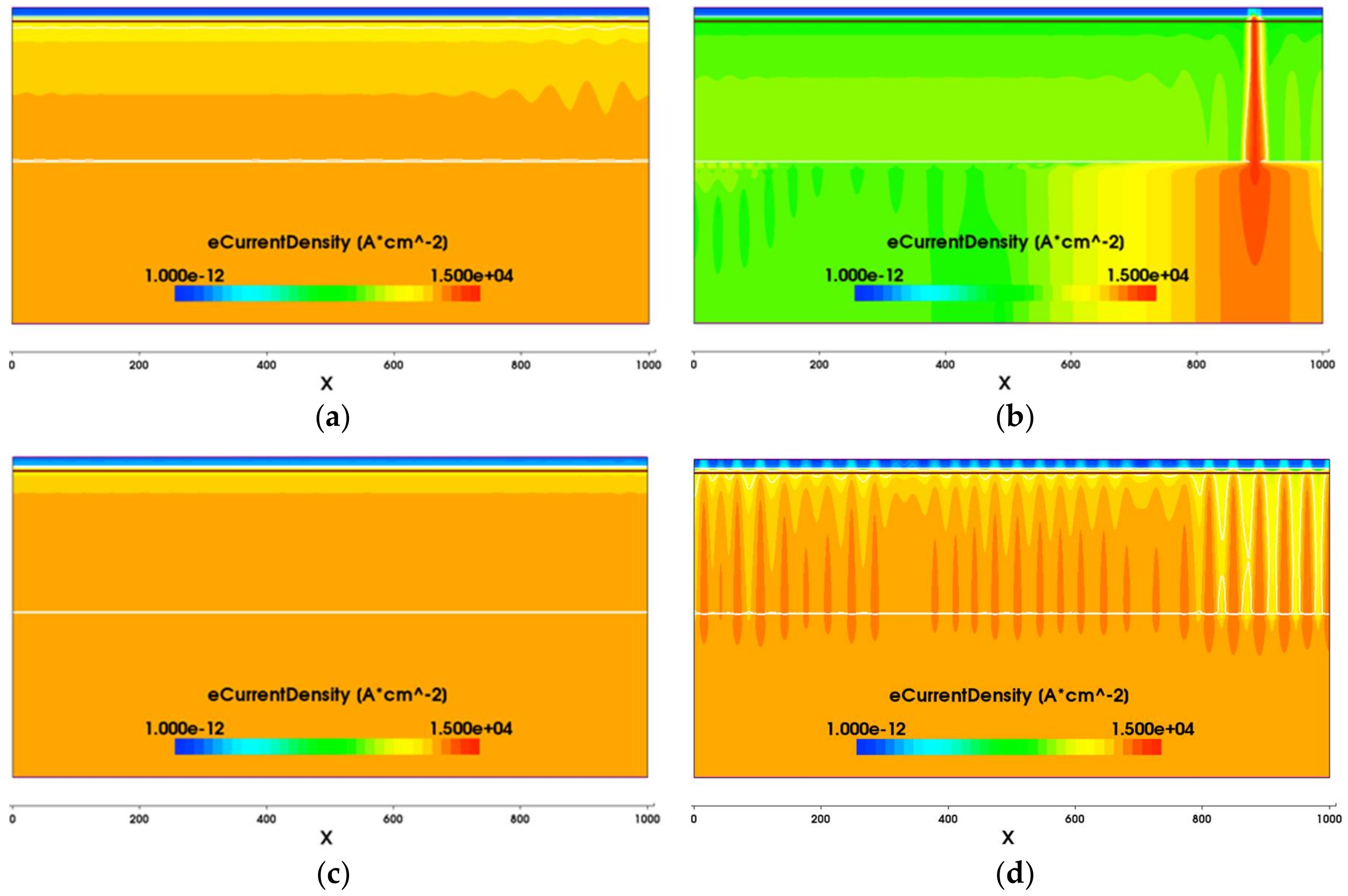
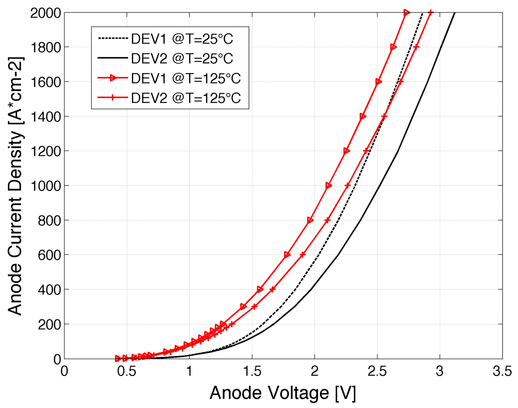
4.3. Wide Area Simulaitons
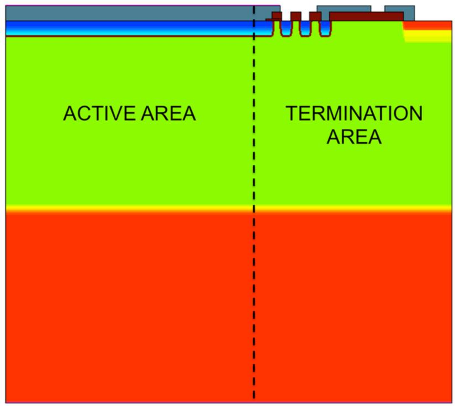
4.4. Effect of Termination Region
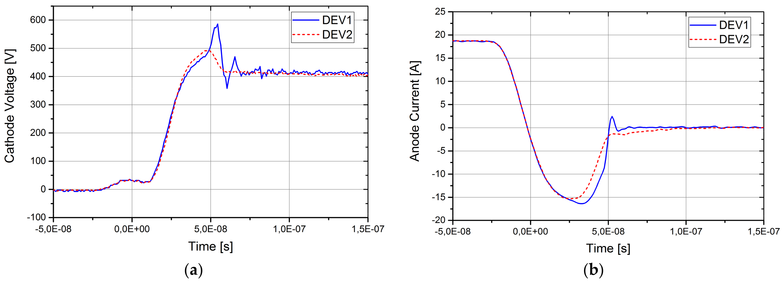
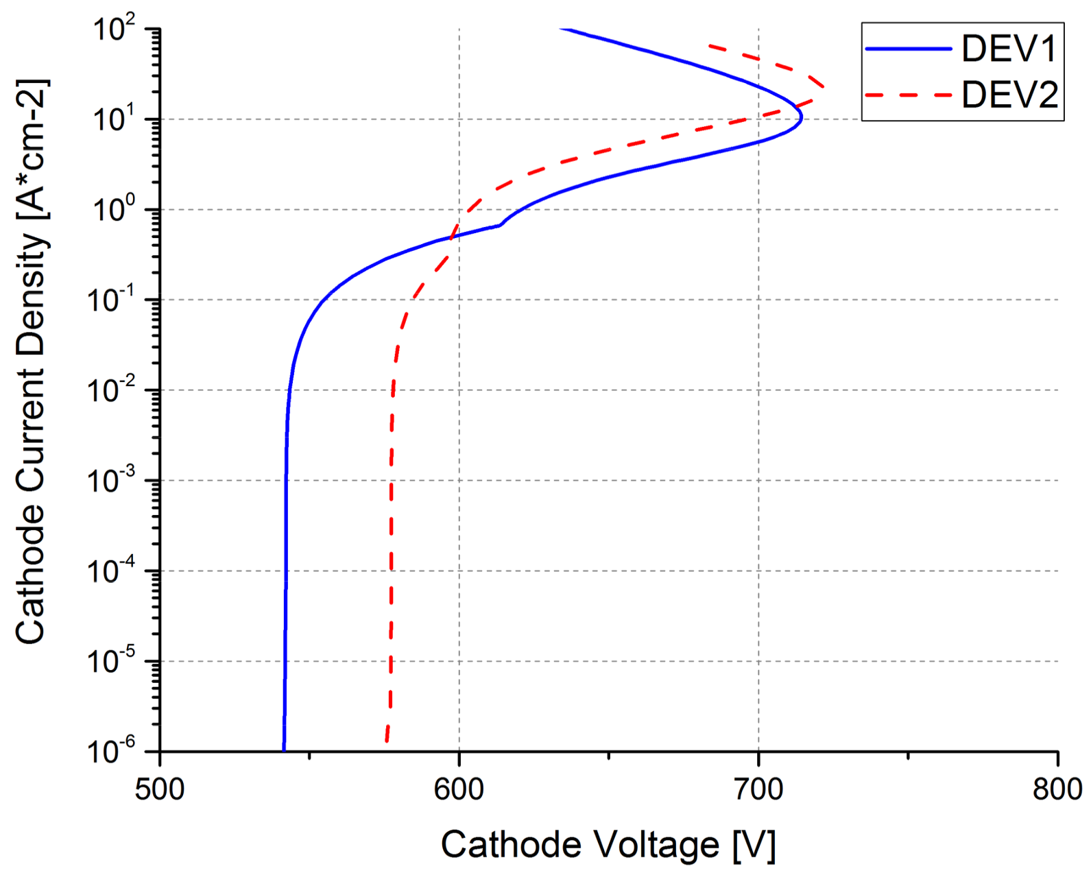
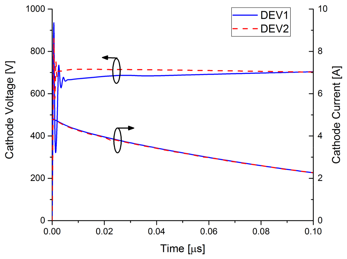
5. Experimental Results
6. Conclusions
Author Contributions
Conflicts of Interest
References
- Lutz, J.; Schlangenotto, H.; Scheuermann, U.; De Doncker, R. Semiconductor Power Devices: Physics, Characteristics, Reliability; Springer Science & Business Media: Berlin, Germany, 2011; pp. 159–224. ISBN 978-3-319-70917-8. [Google Scholar]
- ESD Association. ESD STM5.1-2007: Electrostatic Discharge Sensitivity Testing—Human Body Model; ESD Association: Rome, NY, USA, 2007. [Google Scholar]
- Baburske, R.; Lutz, J.; Heinze, B. Effects of negative differential resistance in high power devices and some relations to DMOS structures. In Proceedings of the 2010 IEEE International Reliability Physics Symposium (IRPS), Anaheim, CA, USA, 2–6 May 2010; pp. 162–169. [Google Scholar]
- Maresca, L.; Romano, G.; Breglio, G.; Irace, A. Physically based analytical model of the blocking I–V curve of Trench IGBTs. Microelectron. Reliab. 2013, 53, 1783–1787. [Google Scholar] [CrossRef]
- Spirito, P.; Breglio, G.; Irace, A.; Maresca, L.; Napoli, E.; Riccio, M. Physics of the Negative Resistance in the Avalanche Curve of Field Stop IGBTs: Collector Design Rules for Improved Ruggedness. Electron. Devices IEEE Trans. 2014, 61, 1457–1463. [Google Scholar] [CrossRef]
- Spirito, P.; Maresca, L.; Riccio, M.; Breglio, G.; Irace, A.; Napoli, N. Effect of the collector design on the IGBT avalanche ruggedness: A comparative analysis between punch-through and field-stop devices. Electron. Devices IEEE Trans. 2015, 62, 2535–2541. [Google Scholar] [CrossRef]
- Breglio, G.; Irace, A.; Napoli, E.; Riccio, M.; Spirito, P. Experimental detection and numerical validation of different failure mechanisms in IGBTs during unclamped inductive switching. Electron. Devices IEEE Trans. 2013, 60, 563–570. [Google Scholar] [CrossRef]
- Irace, A.; Breglio, G.; Spirito, P.; Bricconi, A.; Raffo, D.; Merlin, L. Effect of a buffer layer in the epi-substrate region to boost the avalanche capability of a 100 V Schottky diode. Microelectron. Reliab. 2006, 46, 1784–1789. [Google Scholar] [CrossRef]
- Irace, A.; Spirito, P.; Riccio, M.; Breglio, G. Voltage drops, sawtooth oscillations and HF bursts in Breakdown Current and Voltage waveforms during UIS experiments. In Proceedings of the 24th International Symposium on Power Semiconductor Devices and ICs, Bruges, Belgium, 3–7 June 2012; pp. 165–168. [Google Scholar]
- Vashchenko, V.A.; Shibkov, A. ESD Design for Analog Circuits; Springer Science & Business Media: Berlin, Germany, 2010. [Google Scholar]
- Wachutka, G. Analytical model for the destruction mechanism of GTO-like devices by avalanche injection. Electron. Devices IEEE Trans. 1991, 38, 1516–1523. [Google Scholar] [CrossRef]
- Sun, S.C.; Plummer, J.D. Electron mobility in inversion and accumulation layers on thermally oxidized silicon surfaces. Solid-State Circuits IEEE J. 1980, 15, 562–573. [Google Scholar] [CrossRef]
- Duvvury, C.; Carvajal, F.; Jones, C.; Briggs, D. Lateral DMOS design for ESD robustness. In Proceedings of the 1997 IEEE International Electron Devices Meeting (IEDM’97 Technical Digest), Washington, DC, USA, 10 December 1997. [Google Scholar]
- Rigato, M.; Fleury, C.; Heer, M.; Capriotti, M.; Simbürger, W.; Pogany, D. ESD characterization of multi-finger RF nMOSFET transistors by TLP and transient interferometric mapping technique. Microelectron. Reliab. 2015, 55, 1471–1475. [Google Scholar] [CrossRef]
- Chirilă, T.; Kaindl, W.; Reimann, T.; Rüb, M.; Wahl, U. Analysis of the role of the parasitic BJT of Super-Junction power MOSFET under TLP stress. Microelectron. Reliab. 2015, 55, 1481–1485. [Google Scholar] [CrossRef]
- Irace, A.; Maresca, L.; Mirone, P.; Riccio, M.; Breglio, G.; Bellemo, L.; Carta, R.; Naretto, M.; El Baradai, N.; Para, L.; et al. 200 V Fast Recovery Epitaxial diode with superior ESD capability. Microelectron. Reliab. 2016, 64, 440–446. [Google Scholar] [CrossRef]
- Hower, P.L.; Reddi, V.K. Avalanche injection and second breakdown in transistors. Electron. Devices IEEE Trans. 1970, 17, 320–335. [Google Scholar] [CrossRef]
- Chynoweth, A.G. Ionization rates for electrons and holes in silicon. Phys. Rev. 1958, 109, 1537. [Google Scholar] [CrossRef]
- Mirone, P.; Maresca, L.; Riccio, M.; Breglio, G.; Irace, A. On the avalanche ruggedness of optimized termination structure for 600 V punch-through IGBTs. Microelectron. Reliab. 2016, 58, 17–25. [Google Scholar] [CrossRef]
- Rahimo, M.T.; Shammas, N.Y. Freewheeling diode reverse-recovery failure models in IGBT applications. IEEE Trans. Ind. Appl. 2001, 37, 661–670. [Google Scholar] [CrossRef]


| Test | Test Conditions | DEV1 | DEV2 |
|---|---|---|---|
| UIS | Median (Avalanche current@Tc = 25 °C - L = 1 mH) (A) | 8.8 | 13.6 |
| UIS | Median (Avalanche current@Tc = 25 °C - L = 10 mH) (A) | 4.2 | 5.3 |
| UIS | Median (Avalanche current@Tc = 25 °C - L = 40 mH) (A) | 2.7 | 3.6 |
| Current Pulse | Median (Square pulse avalanche current@Tc = 25 °C, tp = 5 µs) (A) | 5.8 | 8.4 |
| ESD | Fail@2 kV | 0/10 | 0/10 |
| ESD | Fail@4 kV | 0/10 | 0/10 |
| ESD | Fail@6 kV | 1/10 | 0/10 |
| ESD | Fail@8 kV | - | 0/10 |
| VON | Variation compared to DEV1 | - | +5.4% |
| VBR | Variation compared to DEV1 | - | −8% |
© 2018 by the authors. Licensee MDPI, Basel, Switzerland. This article is an open access article distributed under the terms and conditions of the Creative Commons Attribution (CC BY) license (http://creativecommons.org/licenses/by/4.0/).
Share and Cite
Maresca, L.; De Caro, G.; Romano, G.; Riccio, M.; Breglio, G.; Irace, A.; Bellemo, L.; Carta, R.; El Baradai, N. Novel Cathode Design to Improve the ESD Capability of 600 V Fast Recovery Epitaxial Diodes. Energies 2018, 11, 832. https://doi.org/10.3390/en11040832
Maresca L, De Caro G, Romano G, Riccio M, Breglio G, Irace A, Bellemo L, Carta R, El Baradai N. Novel Cathode Design to Improve the ESD Capability of 600 V Fast Recovery Epitaxial Diodes. Energies. 2018; 11(4):832. https://doi.org/10.3390/en11040832
Chicago/Turabian StyleMaresca, Luca, Giuseppe De Caro, Gianpaolo Romano, Michele Riccio, Giovanni Breglio, Andrea Irace, Laura Bellemo, Rossano Carta, and Nabil El Baradai. 2018. "Novel Cathode Design to Improve the ESD Capability of 600 V Fast Recovery Epitaxial Diodes" Energies 11, no. 4: 832. https://doi.org/10.3390/en11040832