Next Article in Journal
Experimental Investigation of a Three-Bed Adsorption Refrigeration Chiller Employing an Advanced Mass Recovery Cycle
Next Article in Special Issue
Dye-Sensitized Solar Cells Based on the Principles and Materials of Photosynthesis: Mechanisms of Suppression and Enhancement of Photocurrent and Conversion Efficiency
Previous Article in Journal
A Preliminary Investigation of Energy Return on Energy Investment for Global Oil and Gas Production
 
 
Addendum published on 26 August 2009, see Energies 2009, 2(3), 695-696.
Review

A Review of Ultrahigh Efficiency III-V Semiconductor Compound Solar Cells: Multijunction Tandem, Lower Dimensional, Photonic Up/Down Conversion and Plasmonic Nanometallic Structures

by
Katsuaki Tanabe
1,2
1
Institute of Industrial Science, University of Tokyo, Tokyo 153–8505, Japan
2
Institute for Nano Quantum Information Electronics, University of Tokyo, Tokyo 153–8505, Japan
Energies 2009, 2(3), 504-530; https://doi.org/10.3390/en20300504
Submission received: 26 June 2009 / Revised: 7 July 2009 / Accepted: 7 July 2009 / Published: 13 July 2009
(This article belongs to the Special Issue Solar Cells)

Abstract

:
Solar cells are a promising renewable, carbon-free electric energy resource to address the fossil fuel shortage and global warming. Energy conversion efficiencies around 40% have been recently achieved in laboratories using III-V semiconductor compounds as photovoltaic materials. This article reviews the efforts and accomplishments made for higher efficiency III-V semiconductor compound solar cells, specifically with multijunction tandem, lower-dimensional, photonic up/down conversion, and plasmonic metallic structures. Technological strategies for further performance improvement from the most efficient (Al)InGaP/(In)GaAs/Ge triple-junction cells including the search for 1.0 eV bandgap semiconductors are discussed. Lower-dimensional systems such as quantum well and dot structures are being intensively studied to realize multiple exciton generation and multiple photon absorption to break the conventional efficiency limit. Implementation of plasmonic metallic nanostructures manipulating photonic energy flow directions to enhance sunlight absorption in thin photovoltaic semiconductor materials is also emerging.

Graphical Abstract

1. Introduction

The current world consumption of electric energy is around 12–13 TW and the earth receives more solar energy in one hour than the energy used globally in one year, considering the solar constant 1.7 × 10⁵ TW at the top of the earth’s atmosphere [1]. However the solar energy incidence, around 1 kW/m2, is quite dilute and thus a vast area of energy converters would be required to meet the world’s energy consumption. Therefore high efficiency solar energy conversion is crucial. Solar cells, also called photovoltaics, are devices that convert sunlight energy into electricity by the photovoltaic effect discovered by the French scientist Henri Becquerel in 1839. Electron–hole pairs are generated by the energy of the incident photons overcoming the energy bandgap of the photovoltaic material to make a current flow according to the built-in potential slope in the material. Solar cells have been recognized as an important alternative power source especially since the oil crises in the 1970s. Solar cells are also promising as a carbon-free energy source to suppress the global warming.
The energy conversion efficiency of a solar cell is defined as the ratio of the electric power generated by the solar cell to the incident sunlight energy into the solar cell per time. Currently in laboratories the highest reported cell efficiencies are around 40%, while the energy conversion efficiencies for thermal power generation can exceed 50%. This fact however does not mean that thermal generation is superior since its resources such as fossil fuels are limited, while solar energy is essentially unlimited. The incident energy flux spectrum of sunlight for reported solar cell efficiencies is standardized as some specifically defined spectra such as Air Mass 0 (AM0), Air Mass 1.5 Global and Direct (AM1.5G and AM1.5D) [2,3,4]. Figure 1 shows the AM1.5G spectrum, most commonly referred for terrestrial-use solar cells under non-concentrated sunlight spectrum measurements. The solar spectrum widely ranges through 300 nm to 2,000 nm with its peak around at 500–600 nm and a large fraction stems from the visible range. The dips prominently observed around at 1,100 nm, 1,400 nm etc. are due to the absorption, mainly by CO2 and H2O, in the atmosphere. The energy fraction of the solar spectrum utilized by an ideal single-junction (i.e., one p-n junction equipped) solar cell with an energy bandgap of 1.4 eV determined by the detailed balance limit calculation representing the thermodynamical solar energy conversion efficiency limit developed by Shockley and Queisser [5] is shown in Figure 1. The area ratio of this energy generation spectrum by the solar cell to the solar irradiation spectrum corresponds to the energy conversion efficiency and is 31% in this case. Concentration of sunlight into a smaller incident area using lenses has two advantages for solar cell applications. The first is the material cost reduction with smaller area of cells required to generate the same amount of energy. The second is the efficiency enhancement with the higher open-circuit voltage VOC increasing logarithmically with the ratio of the photocurrent to the constant dark or recombination current, while the photocurrent simply increases in proportion to solar concentration. However, too much sunlight concentration would rather reduce VOC with increased temperature and also induce significant power loss by the series resistance. There is therefore an optimized concentration factor for each solar cell, practically a couple of hundred suns. Although this paper will not discuss the details of concentrators, interested readers can refer [6,7,8].
Figure 1. Solar irradiation spectrum of AM1.5G, 1 sun and energy utilization spectrum by a single-junction solar cell with an energy bandgap of 1.4 eV. Calculated energy conversion efficiency η = 31.3%.
Energies 02 00504 g001
In this paper, we focus on solar cells made of III-V semiconductor compounds since these types of solar cells have exhibited the leading energy conversion efficiencies, rather than the other materials represented by silicon [9]. Besides the potential for high efficiency, III-V semiconductor compound materials have advantages including the bandgap tunability by elemental compositions, higher photon absorption by the direct bandgap energies, higher resistivity against high-energy rays in space, and smaller efficiency degradation by heat than Si solar cells. The energy conversion efficiencies of III-V solar cells have been steadily increasing year-to-year and are approaching 40% for the laboratory-scale cells, as seen in Figure 2 [10]. A lot of efforts have been made to date to improve the cell performance further for the purpose of the development of space activities and as a solution for the upcoming energy crisis and global environmental issues. In this paper, key factors recently being studied intensively for performance enhancement of III-V semiconductor compound solar cells were selected for review. The principle, history and recent developments of multijunction III-V solar cells are described in Section 2. Section 3 focuses on the fabrication and characteristics of the materials with bandgap energies around 1.0 eV, one of the most critical issues for the further development of III-V multijunction cells in the near future. An overview of the strategies for effective use of higher and lower energy photons than the photovoltaic materials’ bandgaps is given in Section 4 and Section 5, respectively. Newly emerging solar cells with plasmonic metallic nanostructures manipulating photonic energy flow directions to enhance sunlight absorption in thin photovoltaic semiconductor materials is are introduced in Section 6.
Figure 2. Chronological record energy-conversion efficiencies of solar cells. Two latest highest records have been added to the “Best Research-Cell Efficiencies” table available at http://en.wikipedia.org/wiki/Solar_cell. Originally generated by Sarah R. Kurtz, Lawrence L. Kazmerski et al. at National Renewable Energy Laboratory/National Center for Photovoltaics (as a work of the U.S. federal government, the image is in the public domain).
Energies 02 00504 g002

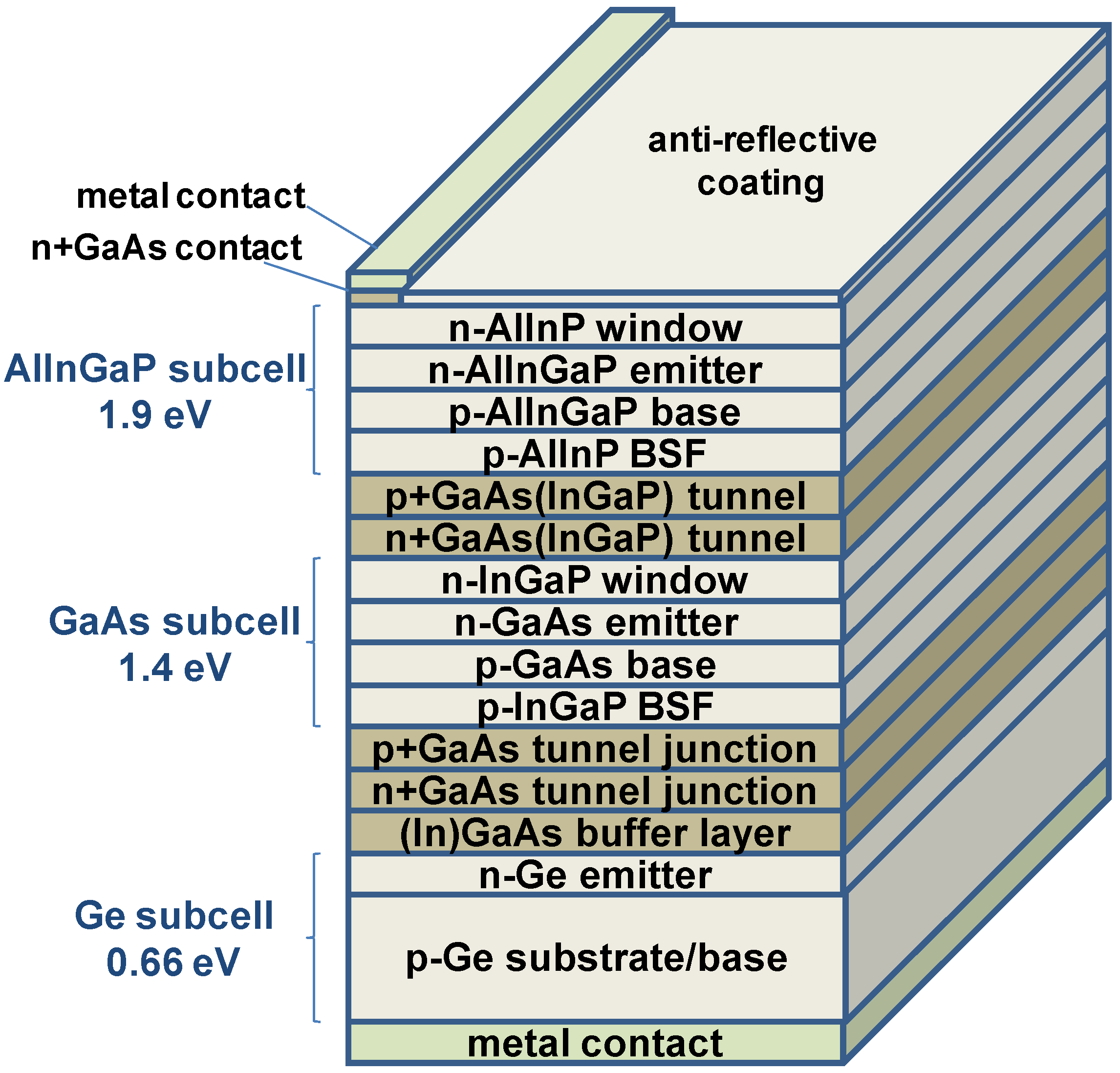
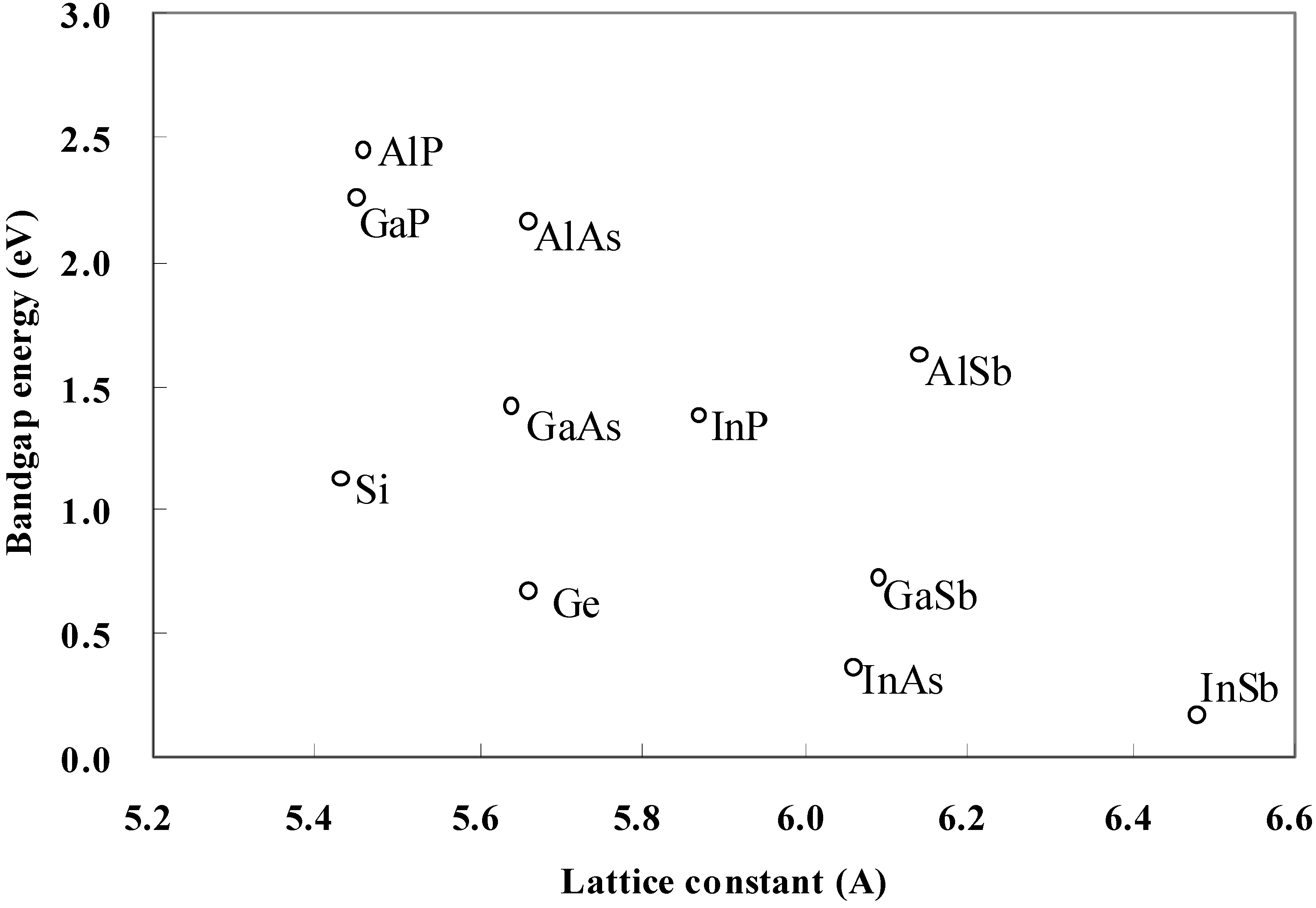
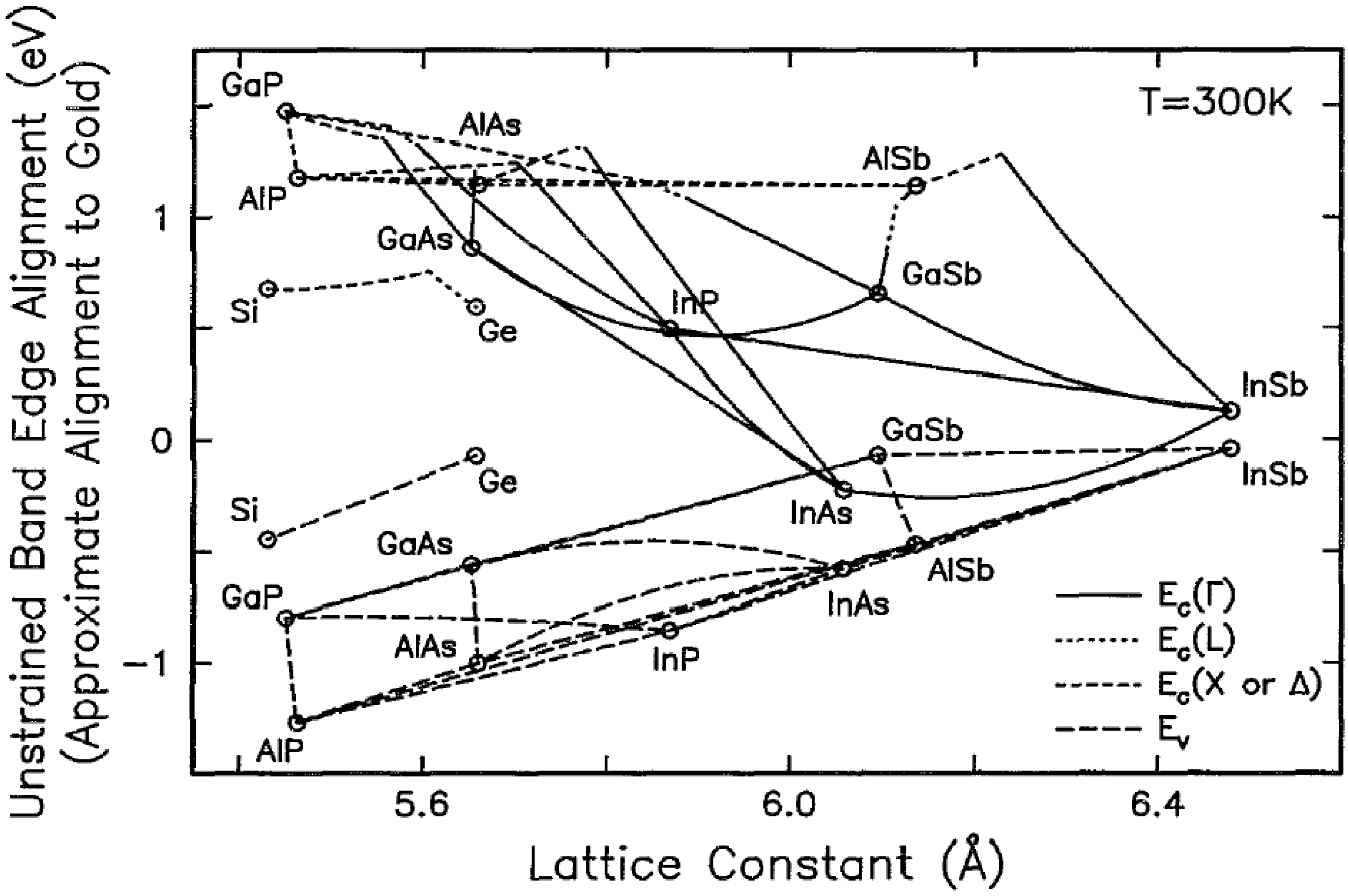
2. Developments of Multijunction III-V Solar Cells

One of the major factors of energy loss in a solar cell is the gap between the photon energy and the bandgap energy Eg of the photovoltaic material. No absorption would occur if the photon energy was smaller than the bandgap energy and merely the part equal to the bandgap energy out of the photon energy could be extracted as electric power leaving the other part wasted as heat if larger. Multistacking of photovoltaic materials of different bandgap energies is therefore commonly used for high efficiency III-V solar cells to reduce this energy loss and absorb the photon energy from the sunlight spectrum more widely and efficiently, taking advantage of the tunability of bandgap energies and lattice constants with the compositions of III-V semiconductor compounds, called multijunction or tandem cells. For instance, Figure 3 shows an energy utilization spectrum for a series-connected AlInGaP (1.9 eV) / GaAs (1.4 eV) / Ge (0.66 eV) triple-junction solar cell calculated as 50.1% efficient with Shockley and Queisser’s detailed balance limit scheme under 1,000 sun concentration (41.4% under AM1.5G, 1 sun), exhibiting significantly higher efficiency represented by the spectral coverage relative to single-junction solar cells, e.g., Figure 1. A detailed balance limit calculation estimated by Henry shows that a 36-gap or -junction cell ideally would reach 72% efficiency at a concentration of 1,000 suns relative to the 37% for a 1-gap cell [11]. A theoretical calculation for the ideal efficiencies according to the bandgap energy combinations of the top and bottom semiconductor materials in dual-junction (2J) solar cells are mapped in Figure 4 [12]. Similar calculations under different conditions are found in [13,14].
Figure 3. Solar irradiation spectrum of AM1.5D, 1,000 suns and energy utilization spectrum by a series-connected AlInGaP (1.9 eV) / GaAs (1.4 eV) / Ge (0.66 eV) triple-junction solar cell calculated with the “detailed balance limit” scheme with current-match restriction. Calculated energy conversion efficiency η = 50.1% (η = 41.4% under AM1.5G, 1 sun).
Energies 02 00504 g003
For multijunction cells, series-connected or two-terminal monolithic structures are generally favored and used rather than expensive and impractical three- or four-terminal structures [15]. A schematic cross-sectional diagram of a monolithic 3J solar cell structure is shown in Figure 5. Multijunction solar cells have been layered by epitaxial growth generally with metalorganic chemical vapor deposition (MOCVD) requiring lattice matching among the stacked semiconductor materials [16,17,18,19]. Figure 6 and Figure 7 [20] show the relation between the lattice constants and the bandgap energies for commonly used III-V semiconductor compounds.
One of the most common and highest efficiency two 2J cells consists of a combination of In0.49Ga0.51P and GaAs with the same lattice constant of 5.64 Å and the bandgap energy of 1.86 eV and 1.42 eV, respectively [21,22,23]. This InGaP/GaAs cell has the highest efficiency of 30.3% under AM1.5G solar spectrum with 1-sun intensity (100 mW cm-2) among monolithic 2J cells [9,23], while 4-terminal configuration allowed the highest 2J efficiency of 32.6% under AM1.5D spectrum at 100 suns for a lattice-mismatched GaAs/GaSb stack (GaSb: 6.09 Å, 0.70 eV) [24]. Quite recently, a 32.6% efficient monolithic InGaP/GaAs 2J cell under AM1.5D at 1000 suns has been also reported [25].
Figure 4. Calculated isoefficiency map for dual-junction four-terminal solar cells under AM1.5G spectrum at one-sun illumination according to the top and bottom cell bandgaps (reprinted from [12]; © 1992, with permission from The Japan Society of Applied Physics).
Energies 02 00504 g004
Figure 5. Cross-sectional schematic of a triple-junction cell structure.
Energies 02 00504 g005
Figure 6. Bandgap energies plotted as a function of the lattice constant of semiconductors.
Energies 02 00504 g006
Figure 7. Conduction band edge and valence band edge energies plotted as a function of the lattice constant of semiconductors. The zero energy point represents the approximate gold Schottky barrier position in the band gap of any given alloy (reused with permission from [20]; © 1992, American Institute of Physics).
Energies 02 00504 g007
For 3J cells, the most common so far, a Ge bottom cell is added to the InGaP/GaAs 2J cell to form an InGaP/GaAs/Ge structure for Ge’s lattice constant of 5.66 Å nearly equal to that of InGaP/GaAs. This 3J structure is grown on a Ge substrate and an advantage that Ge is a cheaper and mechanically stronger material than GaAs relative to cells grown on GaAs substrates. Spectrolab, a leading manufacturer of high performance III-V cells, presented a lattice-matched In0.495Ga0.505P/In0.01Ga0.99As/Ge 3J cell with a 39.0% efficiency at 236 suns under AM1.5D in 2005 [26,27] followed by a metamorphic (i.e., slightly lattice-mismatched) In0.56Ga0.44P/In0.08Ga0.92As/Ge with 40.7% at 240 suns in 2007 [28,29]. Higher indium content in top InGaP and middle InGaAs subcells pulls their bandgap energies down and increases photocurrent in those subcells to obtain a better current-matching to the bottom Ge subcell. Fraunhofer Institute have achieved a 41.1% efficiency at 454 suns under AM1.5D with a metamorphic In0.65Ga0.35P/In0.17Ga0.83As/Ge 3J cell in 2009 [30].
Solar cell efficiency records have been generated mostly indeed with InGaP/(In)GaAs/Ge 3J and its derivative InGaP/(In)GaAs/InGaAs, discussed in the next section, structures in the past twenty years. The efficiency record is this way is still being increased little by little and year by year just by modifications of this InGaP/GaAs/Ge 3J system. However, it should be noted that the 0.66 eV bandgap energy of Ge is not optimal as the material for the bottom subcell in a 3J cell. This point will be discussed in the following section.
Specifically for the space use, very thin, light and flexible InGaP/GaAs 2J and InGaP/GaAs/Ge 3J cells are being developed recently [31,32,33]. Figure 8 shows a photograph of a flexible InGaP/GaAs 2J device [33]. Although the fabrication processes have not been well disclosed, the photovoltaic layers are attached to metal or polymer supporting films and the parent substrates for the epitaxial growth are removed somehow.
Figure 8. Photograph of a flexible thin-film InGaP/GaAs dual-junction 4 × 7 cm2 film-laminated cell (reprinted from [33]; © 2006, with permission from IEEE).
Energies 02 00504 g008
For further improvement of the cell efficiency, cells with more junctions are being proposed such as an InGaP/GaAs/InGaAsN/Ge four-junction (4J) structure [34], which will be also discussed in the following section. Recently an (Al)InGaP/InGaP/Al(In)GaAs/(In)GaAs/InGaAsN/Ge 6J cell has been demonstrated [35]. The efficiency of this 6J cell was 23.6% under AM0 at 1 sun (135 mW cm-2). (Note that the intensities of 1 sun for AM1.5 and AM0 are different. See [4,36] for the detail of the standard artificial solar spectra for cell measurements.) This efficiency is much lower than the highest efficiency 3J cell regardless of more number of junctions presumably due to the current-limiting InGaAsN layer with low quantum efficiency. VOC of this 6J cell was however 5.33 V, significantly higher than the 3.09 V of the highest efficiency 3J cell, simply because of the series connection of six semiconductor materials.
In-Ga-N nitride compound solar cells have been proposed and are currently being studied for the requirement of high-Eg top subcells, with Eg higher than 1.8 eV of In0.49Ga0.51P, for >3J multijunction stacking [37,38,39,40]. A fascinating advantage for this In-Ga-N system is its wide range of available Eg, from 0.7 eV of InN to 3.4 eV of GaN [41]. Incorporation of aluminum forming Al-In-Ga-N would lift the upper edge even further, up to 6.2 eV for AlN. For quaternary compounds, lattice-matched multijunction cells could be constructed in principle by their independent tunability of lattice constants and bandgap energies, while their growth with proper dislocation densities and p/n doping looks still challenging at this point.
A collaborative US team based on a Defense Advanced Research Projects Agency’s (DARPA) program are working on a novel type of solar cell module with sunlight spectral splitting by dichroic filters and independently located cells with varied bandgap energies [42,43]. In this architecture, each cell will receive a fraction of the solar spectrum most efficiently absorbed and converted into electrical power and can avoid the current-matching issue among subcells and free carrier absorption loss [44,45,46] in upper subcells for monolithic devices. They have tested independent InGaP/GaAs 2J, Si 1J and InGaAsP/InGaAs 2J cells without the optical splitting architecture but with proper filters to mimic spectral incidence to each cell and reported a 42.7% efficiency simply by summing up the three cells’ efficiencies to suggest a potential for very high efficiency photovoltaic modules.

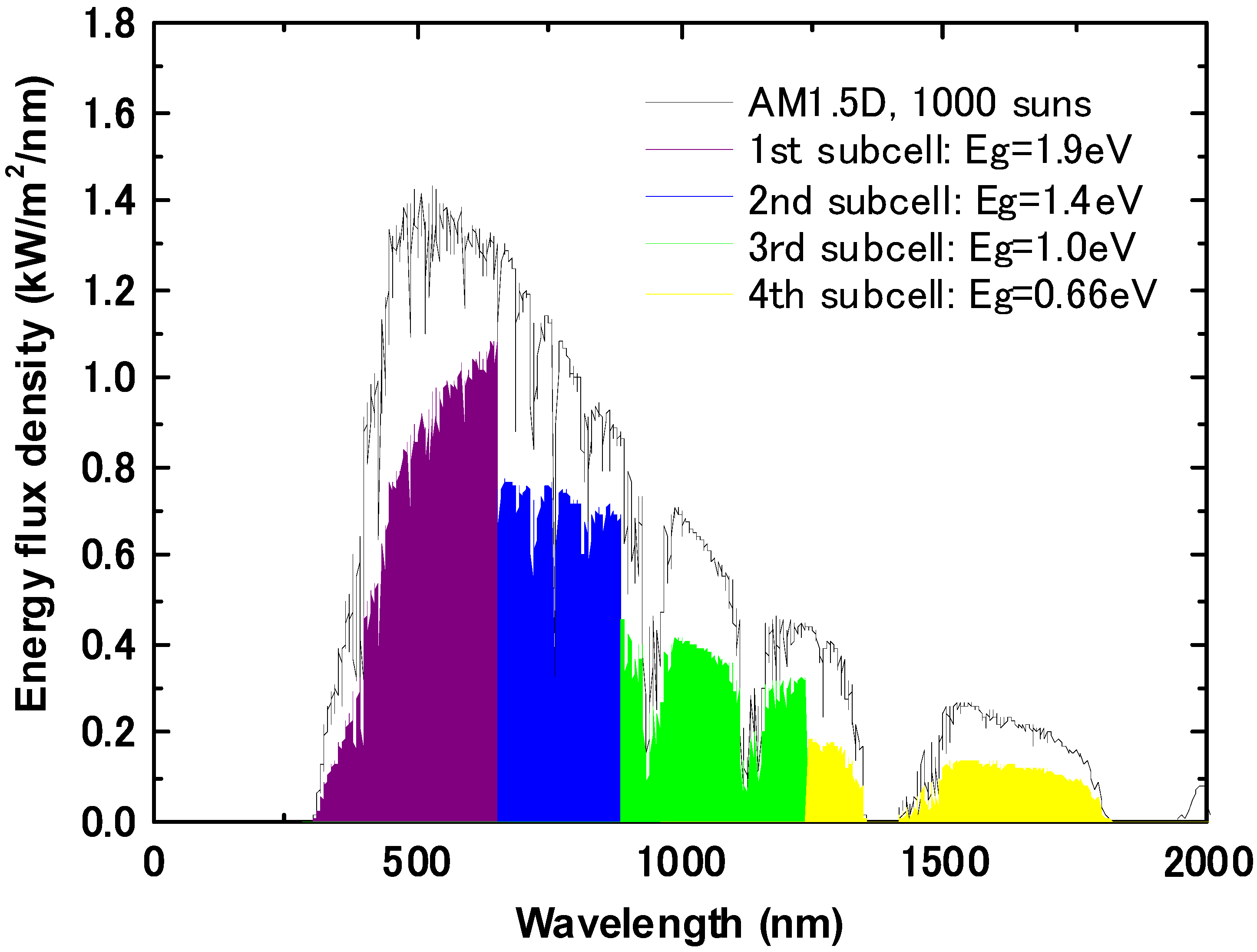
3. 1.0 eV Bandgap Subcells

The optimal bandgap energy for the bottom cells in 3J solar cells is known to be around 1.0 eV considering the current matching among three subcells, assuming the top 2J structure is the (Al)InGaP/GaAs. For example, detailed balance limit calculation for a series-connected AlInGaP (1.9 eV) / GaAs (1.4 eV) / 1.0 eV 3J solar cell under 1,000 suns gives a 55.0% efficiency, higher than 50.1% for an AlInGaP/GaAs/Ge cell in Figure 3, with an excellent current matching (Figure 9) (44.4% under AM1.5G, 1 sun). Therefore materials of ~1.0 eV bandgap lattice-matched to GaAs and Ge have been intensively researched. As well as replacing the Ge subcell with a 1.0 eV bandgap material, insertion of a 1.0 eV material between the GaAs and Ge subcells would also improve the efficiency. The detailed balance limit efficiency of a series-connected AlInGaP (1.9 eV) / GaAs (1.4 eV) / 1.0 eV / Ge (0.66 eV) 4J solar cell under 1,000 suns is calculated as 60.9% (Figure 10) (47.7% under AM1.5G, 1 sun). The GaAs middle subcell in an InGaP/GaAs/Ge 3J cell limits the overall photocurrent (i.e., has the smallest photocurrent among the three subcells) and therefore an increase of the InGaP top subcell bandgap by adding Al and increasing Al content in the AlInGaP quaternary would improve the efficiency. However addition of Al induces a significant reduction of the photocurrent of the InGaP cell probably due to the adverse effect of Al and the associated oxygen contamination on minority-carrier properties [47]. Lowering the bandgap of the current-limiting GaAs middle subcell by substituting a portion of the Ga content with In is another approach for higher efficiency than the InGaP/GaAs/Ge 3J cell, although this approach accompanies lattice mismatch and requires graded buffer layers or suffers from large density of dislocations otherwise [27,48]. Thinning of the InGaP subcell to pass a fraction of photons to the GaAs subcell is an alternative, moderate solution [13].
Figure 9. Solar irradiation spectrum of AM1.5D, 1,000 suns and energy utilization spectrum by a series-connected AlInGaP (1.9 eV) / GaAs (1.4 eV) / 1.0 eV triple-junction solar cell calculated with the “detailed balance limit” scheme with current-match restriction. Calculated energy conversion efficiency η = 55.0% (η = 44.4% under AM1.5G, 1 sun).
Energies 02 00504 g009
InxGa1-xAs1-yNy can be lattice matched to GaAs for compositions satisfying x = 3y and can have a bandgap of ~1.0 eV [49]. Although this InGaAsN has been thought to be the most promising candidate, its minority carrier diffusion length has been too short, resulting low output photocurrent [50,51,52]. Other candidates such as ZnGeAs2, GaTlP2 and InGaAsB have not shown very promising properties either [15].
Sb has been recently incorporated in the nitride system to form InGaAsNSb cells lattice-matched to GaAs with 0.92 eV bandgap and demonstrated relatively high quantum efficiency and current density enough for current-matching to the InGaP/GaAs cell [53,54]. The low VOC observed at this point obscures advantage of this InGaAsNSb over Ge cells, but improvement of grown crystal quality would be able to push this new compound up to the list of promising candidates.
Figure 10. Solar irradiation spectrum of AM1.5D, 1,000 suns and energy utilization spectrum by a series-connected AlInGaP (1.9 eV) / GaAs (1.4 eV) / 1.0 eV / Ge (0.66 eV) four-junction solar cell calculated with the “detailed balance limit” scheme with current-match restriction. Calculated energy conversion efficiency η = 60.9% (η = 47.7% under AM1.5G, 1 sun).
Energies 02 00504 g010
An alternative is a 1.0 eV InGaAs material lattice-mismatched to GaAs with graded compositions in epitaxial growth [55]. The U.S. National Renewable Energy Laboratory (NREL) grew a ~1 eV InGaAs subcell lattice-mismatched to GaAs by 2.2% on an inversely grown GaAs/InGaP 2J subcell via transparent compositionally graded layers. This epitaxial structure was mounted to a pre-metallized Si supporting wafer and then the parent GaAs substrate was selectively removed resulting an InGaP/GaAs/InGaAs 3J cell [56,57]. This inversely grown cell achieved a 40.8% efficiency under AM1.5D at 140 suns [58] as well as the highest efficiency (as of January 2009 [9]) for AM1.5G, 1 sun condition of 33.8% [59].
Direct wafer bonding could be also used for lattice-mismatched stack. A bonded GaAs/In0.53Ga0.47As monolithic 2J cell with a lattice mismatch of 4% has been prepared, indicating potential for an InGaP/GaAs/InGaAsP/InGaAs 4J cell, as depicted in Figure 11, through bonding of an InGaP/GaAs 2J subcell and an InP-based 1eV-InGaAsP/0.73eV-InGaAs 2J subcell with the 4% lattice mismatch [60]. As a strategy to lower manufacturing costs by reusing expensive III-V semiconductor compound substrates, Ge/Si and InP/Si alternative growth substrates fabricated through wafer bonding and layer transfer of Ge and InP thin films onto Si substrates and growth of InGaP/GaAs 2J and InGaAs 1J cells on each with comparable cell efficiencies relative to cells grown on bulk Ge and InP substrates, respectively, have been demonstrated [61,62].
Figure 11. Cross-sectional schematic of a direct-bonded monolithic lattice-mismatched four-junction solar cell.
Energies 02 00504 g011

4. Utilization of Higher Energy Photons

The most crucial loss mechanism for solar cell efficiency is the energy mismatch between the photons and the bandgap of photovoltaic materials, as mentioned in Section 2. Some concepts to utilize the photons with energy higher and lower than the semiconductor bandgap will be discussed in Section 4 and Section 5.
One method to utilize higher energy photons is multiple carrier excitation from one photon by impact ionization, schematically depicted in Figure 12, the inverse process of Auger recombination [63,64]. This nonlinear phenomenon is more commonly called “multiple exciton generation” or “carrier multiplication”. In semiconductor quantum dots (QDs), also called “nanocrystals”, the carrier cooling rate can be significantly reduced due to the discrete character of the carrier density of states. Also, the impact ionization rate is greatly enhanced because of the moderated momentum-match condition and enhanced Coulomb interaction between excitons due both to the three-dimensional carrier confinement. Multiple carrier excitation can thus be quite efficient in quantum-confined semiconductor QDs, while it is inefficient in bulk semiconductors due to the much faster carrier recombination rate than the impact ionization rate [65]. Currently quantum efficiency enhancement using this multiple carrier excitation process is intensively studied with PbSe, PbS and CdSe QDs using high energy incident optical beam. Surprisingly a quantum efficiency (QE) of 300% [66], excitation of three electron-hole pairs from each incident photon, has been demonstrated with PbSe QDs followed by the even more striking news of a 700% QE in 2006 [67]. They verified generation of more-than-one exciton pairs from each incident photon in QDs through detection of exciton population evolution by time-transient absorption measurements in the time scale of biexciton decay lifetime [64,68,69]. Multiple exciton generation has been observed also in InAs [70,71] and Si [72] QDs.
Figure 12. Schematic energy diagram for impact ionization generating two carrier pairs from each incident photon (reprinted from [63]; © 2002, with permission from Elsevier.)
Energies 02 00504 g012
One issue for efficient utilization of multiple carrier excitation is the existence of the threshold or onset of multiple excition generation in terms of incident photon energy. In most experimental studies, carrier multiplication energy threshold ECM has been observed as significantly higher than naively-expected 2Eg. This phenomenon is even more prominent in bulk semiconductors, where ECM ~ 4Eg provided electron effective mass me ~ hole effective mass mh [73,74], due to the requirement of energy and momentum conservation among carriers involved in impact ionization. Successful ECM reduction down to ~2Eg however has been recently observed utilizing momentum spread and small me/mh ratio in InAs QDs [71]. In this ECM aspect, III-V semiconductor compound QDs can be practically more useful than II-VI QDs for smaller me/mh ratio and stronger exciton-exciton Coulomb coupling due to smaller dielectric constants as well as established device fabrication technologies and circumvent of lead-salts’ toxicity.
Detailed balance limit calculations for solar cell efficiency with multiple carrier excitation have been carried out [75,76,77]. For example, the efficiency limit for single-junction cells generating up to 8 electron-hole pairs from one photon was estimated as 58% under a 1,000-sun illumination (39% for 1 sun) relative to 38% (31% for 1 sun) without multiple carrier excitation with their optimized energy bandgaps assuming ECM ~ 2Eg (Figure 13) [77].
Incidentally, the mechanism for multiple carrier excitation is still unclear and being intensively discussed [78]. Some new physical models for instance are proposed suggesting a contribution from confinement-enhanced Coulomb interactions in nanocrystals and large spectral densities of high-energy single-exciton and multi-exciton states with a claim that such high quantum efficiencies experimentally observed cannot be explained merely by impact ionization [66,79]. Even the existence of multiple carrier excitation process itself is still somewhat controversial [80] because no direct observation of multiple carrier excitation in the shape of photocurrent extracted from a semiconductor has been made yet.
Figure 13. (Left vertical axis) Solar irradiation spectrum of AM1.5D, 1,000 suns and energy utilization spectrum by a single-junction solar cell with the optimized energy bandgap to obtain the maximum efficiency for each case with and without multiple carrier excitation (MCE). Eg = 0.5 eV, energy conversion efficiency η = 57.6% for the cell with MCE and Eg = 1.1 eV, η = 37.6% for the cell without MCE. (Right vertical axis) The carrier multiplication factor at each wavelength for the cell with MCE was also plotted.
Energies 02 00504 g013
Another idea to utilize of higher energy photons is to induce emission of two lower-energy photons from incident of one higher-energy photon by introduce an impurity level in the bandgap of the photovoltaic material. This concept is called down-conversion and was demonstrated in Eu3+-doped LiGdF4 emitting two visible photons for each absorbed UV photon through a two-step energy transfer from excited Gd3+ into Eu3+ emitting two photons [81]. It is suggested that III-V semiconductor compounds such as AlAs and GaP doped with proper impurities could be down-converters [82]. A similar down-converting process has been recently demonstrated in Si QDs with Er3+ ions in SiO2 matrices [83].

5. Utilization of Lower Energy Photons

An emerging idea is to utilize the photons with lower energy than the bandgap of photovoltaic materials, which would be wasted as heat in conventional solar cells, by up-converting the lower-energy photons into higher energy photons. Two IR photons absorbed by a vitroceramic doped with certain rare earth’s, for instance, could emit one visible photon [84]. Sub-bandgap photons can be utilized by putting such an up-converting material in front of a solar cell or behind a solar cell with a reflector behind the up-converter. This concept was proven for a GaAs cell with a rare-earth-doped vitroceramic up-converter, as depicted in Figure 14, showing power output from IR incident light [85]. The upper limit of cell efficiency with an up-converter was estimated to be 48% and 63% under 1 sun and 46,200 suns, the geometrical concentration limit, respectively [86].
Figure 14. Cross-sectional schematic of the experimental coupling of a substrate-free GaAs solar cell to a vitroceramic doped with Er3+ and Yb3+ (reprinted from [57]; © 1996, with permission from The Japan Society of Applied Physics.)
Energies 02 00504 g014
Figure 15. Schematic energy band diagram of a quantum-well solar cell (reprinted from [63]; © 2002, with permission from Elsevier.)
Energies 02 00504 g015
Another idea to utilize lower-energy incident photons is to add intermediate bands inside the semiconductor photovoltaic material itself rather than an external up-converter described above. Insertion of impurity levels in the bandgap of photovoltaic materials to excite carriers by photons with energies lower than the bandgap is proposed [87,88]. Quantum well (QW) or quantum dot (QD) structures can also enable photons of lower energy than the bandgap of the original photovoltaic material to be absorbed by QWs/QDs with narrower bandgap incorporated in the original material [63,89,90,91]. The carriers or excitons generated in the QWs/QDs can thermally escape onto the conduction band for electrons or valence band for holes to contribute to the total photocurrent enhancement ideally maintaining the photovoltage of the original material, as schematically depicted in Figure 15. Photocurrent enhancement for a GaAs solar cell with InGaAs/GaAs multi-quantum wells (MQWs) relative to a GaAs cell without MQW in the IR region was observed [92]. The efficiency limit for such solar cells with intermediate bands was estimated as 63% under 46000 suns [93], inevitably equal to the value in [86].

6. Plasmonic Nanometallic Structures for Light Absorption Enhancement

Metal nanoparticles are known to exhibit distinctive optical characteristics, such as surface-enhanced Raman scattering (SERS) and second harmonic generation (SHG), relative to the bulk form of metals [94,95,96]. Representatives of the use of metal nanoparticles are biomolecular manipulation, labeling and detection with SERS [97,98]. Other optoelectronic fields inspired by metal nanoparticles are also emerging, such as multiphoton absorption and fluorescence excitation for microscopy, microfabrication and optical data storage [99,100].
These characteristics highly rely on the surface plasmon absorption, an enhanced absorption of light or electromagnetic fields by coupling between the incident photons and collective oscillation of free electrons at the metal surface [101,102]. It was theoretically suggested that electromagnetic energy can be guided along periodic chain arrays of closely spaced metal nanoparticles that convert the optical mode into non-radiating surface plasmons [103]. Such plasmonic devicesexploit light localization in the dipole-dipole coupling, or collective dipole plasmon oscillations of electrons, in neighboring nanoscale metal particles at the plasmon frequency. Plasmon waveguides consisting of closely spaced Ag nanoparticles with diameters around 30 nm have been experimentally observed to guide electromagnetic energy over distances of several hundred nanometers via near-field particle interactions [104]. Furthermore it has been suggested that light can be routed efficiently around sharp corners of nanoparticle chain arrays [105]. Such plasmon waveguide technologies can potentially be utilized for construction of all-optical nanoscale network [106,107,108].
Solar cell structures have been suffering from such a trade-off on the thickness of the active photovoltaic layers as follows. Thinner photovoltaic layers will have less light absorption while thicker layers will have more bulk carrier recombination, as schematically depicted in Figure 16. Both of these two factors would be losses for the solar cell electrical output converted from the incident sunlight energy. Therefore the thickness of the active photovoltaic layer is usually optimized to maximize the energy conversion efficiency through that trade-off. Metallic nanostructures can excite surface plasmons and can dramatically increase the optical path length in thin active photovoltaic layers to enhance overall photoabsorption. In this Section, I describe two schemes to utilize surface plasmons for solar cell applications.
Figure 16. Schematic for the trade-off issue in photovoltaic layer thickness. Thinner photovoltaic layers will have less light absorption (left) while thicker layers will have more bulk carrier recombination (right).
Energies 02 00504 g016
Metal nanoparticles placed on solar cell surfaces can act as “antennas” to collect the incident light with their large extinction cross section near the surface plasmon resonance and then scatter the incident light into a wide range of angles to increase the optical path length in the absorber layer (Figure 17a). This effect has potential for cell cost and weight reduction resulting from use of thinner absorber layers and also for efficiency enhancement associated with increased carrier excitation level. Much higher optical scattering rates over absorption rates can be obtained for noble metal particles to minimize absorption loss by properly choosing particles’ diameters, around 100 nm as a rule of thumb. The ratio of scattering/absorption rates becomes larger for larger particles in the quasistatic limit approximation valid for subwavelength-scale particles, while particles with sizes comparable to or larger than incident wavelengths would suffer from electrodynamic damping to lose the solar energy just as heat generated in the particles. Several research groups have observed photocurrent enhancement for Si cells by this scheme [109,110,111,112,113,114,115]. Applications of such plasmonic metal nanoparticles to other types of solar cells such as dye-sensitized solar cells and organic solar cells have been also reported [116,117,118].
The very same trade-off between the absorption length and the carrier diffusion length exists of course also in III-V semiconductor compound solar cells. A couple of groups have experimentally studied optically-thin GaAs solar cells with arrays of subwavelength-size metal particles on top and observed enhancement in photocurrent particularly in near-IR region and even in overall cell efficiencies [119,120,121].
By placing a metallic layer at the bottom of a photovoltaic layer as schematically depicted in Figure 17b, incident light can couple into surface plasmons propagating at the semiconductor/metal interface via some subwavelength-size feature such as nanoscale grooves [108,122,123,124]. In this way, we can convert the direction of energy flux from normal to lateral direction relative to the photovoltaic layer. This is a novel concept to utilize such surface plasmon propagation for solar cell applications to harvest more energy from the sun in thin photovoltaic active layers [119,125].
Some types of conventional solar cells such as silicon solar cells also have metallic back reflectors to increase optical path, while III-V semiconductor compound solar cells such as GaAs cells have thin photovoltaic active layers on top of thick substrate. However, the plasmon-induced absorption enhancement by metallic back structures observed in this study would occur significantly only for strongly absorbing or direct bandgap semiconductors accounting for the energy dissipation in metals.
Figure 17. Schematic cross-sectional of solar cell structures with (a) metal nanoparticles on top and (b) a back metal layer. (a) Incident sunlight is collected by subwavelength-scale metal particles with their large extinction cross-section and reradiated into semiconductor in multiple angles to increase optical path length in thin film photovoltaic layers. (b) Incident sunlight is incoupled into surface plasmons propagating at the semiconductor/metal interface via subwavelength-size grooves to increase the optical path by switching the light direction from normal to the photovoltaic layer to lateral.
Energies 02 00504 g017
Figure 18. Schematic cross-sectional diagram of the waveguide-like GaAs solar cell with metal back layer.
Energies 02 00504 g018
A calculation for energy dissipation fraction of coupled surface plasmon polaritons propagating at material interfaces into metals and semiconductors showed that most energy is absorbed by GaAs rather than metals for the visible optical wavelength range, which solar cell applications concerns, particularly for the cases with Ag and Al [126]. This result means GaAs can effectively harvest the energy extracted from the coupled surface plasmons beating the Ohmic loss in metals with its strong absorption or large imaginary part of dielectric function. On the other hand, silicon, which is a weak absorber, has much lower energy absorption fraction suffering from Ohmic loss in metals. This is a great benefit for direct bandgap semiconductor materials, which are stronger absorbers, for such types of “plasmonic” solar cell applications. Based on this concept, prototype thin film GaAs solar cells with Ag back layers have been fabricated with net photocurrent enhancement throughout the solar spectral range relative to the reference GaAs cell with an absorbing GaAs back layer (Figure 18) [119]. A peak for the normalized photocurrent around at the GaAs bandedge was found and attributed to multiple-angle reflection at the Ag back layer. Another photocurrent enhancement peak was found at 600 nm and is due either to surface plasmon coupling at the GaAs/Ag interface or Fabry-Perot resonance effect.

7. Conclusions

In this paper, recent developments in the field of III-V semiconductor compound photovoltaics were introduced and possible strategies for further efficiency improvements were discussed. Around-40% efficiencies have already been achieved with multijunction solar cells. For further efficiency improvement, a 1.0 eV bandgap material lattice-matched to GaAs and Ge is currently being sought. Nitrides are the strongest candidates, while suffering from their low quantum efficiencies. Lattice-mismatch strategies are also going on, such as compositionally graded growth and direct wafer bonding. Lower-dimension systems such as quantum well and dot structures are emerging to realize multiple-carrier excitation and multiple-photon absorption to break the conventional efficiency limit. Metal nanoparticles and metallic thin films with subwavelength-scale grooves are expected to assist sunlight absorption in thin film photovoltaics with surface plasmon resonance.

References and Notes

  1. Nozik, A.J. Exciton multiplication and relaxation dynamics in quantum dots: Applications to ultrahigh-efficiency solar photon conversion. Inorg. Chem. 2005, 44, 6893–6899. [Google Scholar] [CrossRef] [PubMed]
  2. Emery, K.A.; Osterwald, C.R. Solar-cell efficiency measurements. Sol. Cells 1986, 17, 253–274. [Google Scholar] [CrossRef]
  3. Nann, S.; Emery, K. Spectral effects on PV-device rating. Sol. Energy Mater. Sol. Cells 1992, 27, 189–216. [Google Scholar] [CrossRef]
  4. Emery, K. Measurement and characterization of solar cells and modules. In Handbook of Photovoltaic Science and Engineering, 1st ed.; Luque, A., Hegedus, S., Eds.; Wiley: New York, NY, USA, 2003; Chapter 16; pp. 701–752. [Google Scholar]
  5. Shockley, W.; Queisser, H.J. Detailed balance limit of efficiency of p-n junction solar cells. J. Appl. Phys. 1961, 32, 510–519. [Google Scholar] [CrossRef]
  6. Campbell, P.; Green, M.A. The limiting efficiency of silicon solar-cells under concentrated sunlight. IEEE Trans. Electron Devices 1986, 33, 234–239. [Google Scholar] [CrossRef]
  7. Andreev, V.M.; Grilikhes, V.A.; Rumyantev, V.D. Photovoltaic Conversion of Concentrated Sunlight, 1st ed.; Wiley: New York, NY, USA, 1997. [Google Scholar]
  8. Swanson, R.M. Photovoltaic Concentrators. In Handbook of Photovoltaic Science and Engineering, 1st ed.; Luque, A., Hegedus, S., Eds.; Wiley: New York, NY, USA, 2003; Chapter 11; pp. 449–503. [Google Scholar]
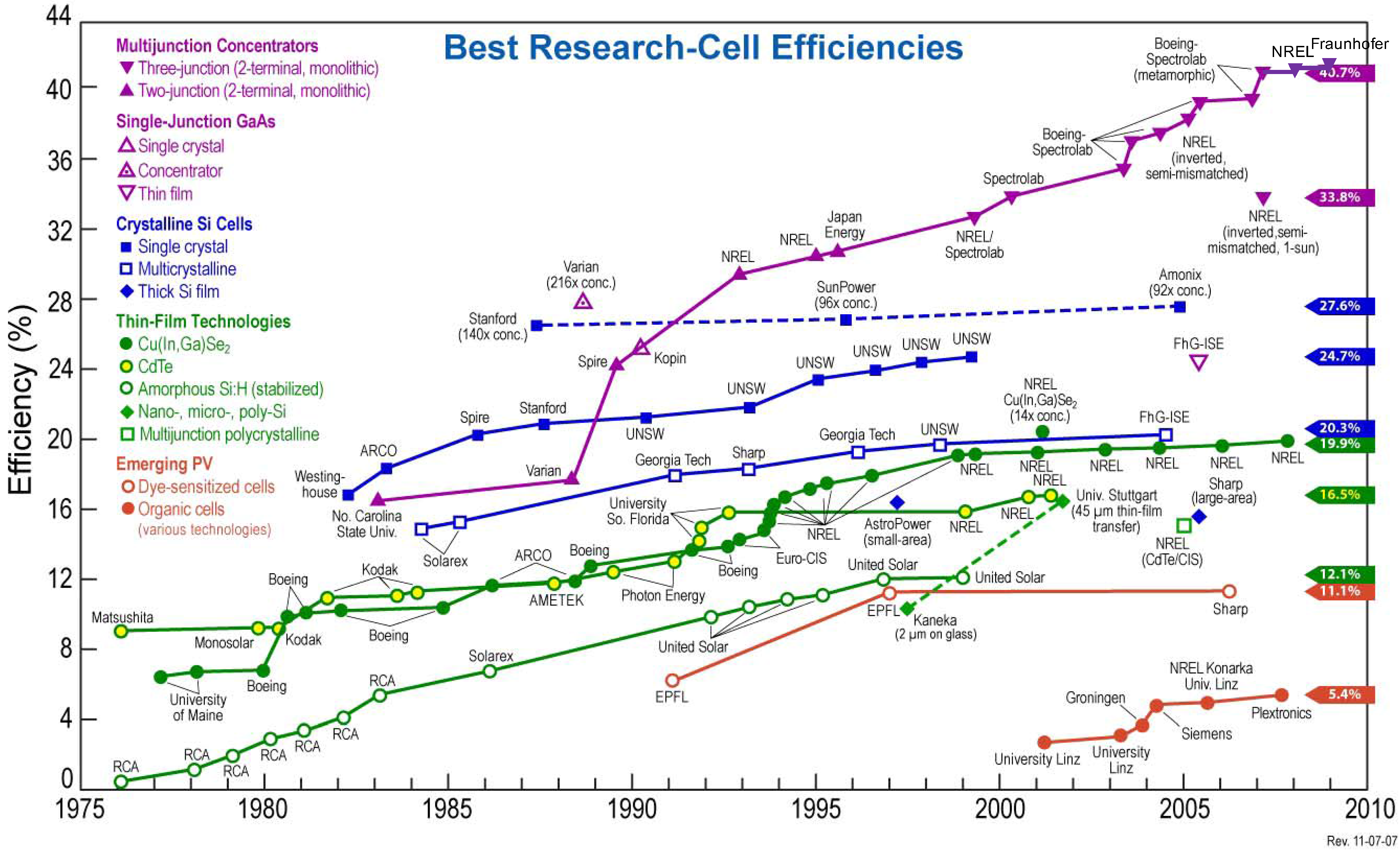
  9. Green, M.A.; Emery, K.; Hishikawa, Y.; Warta, W. Solar cell efficiency tables (version 33). Prog. Photovoltaics Res. Appl. 2009, 17, 85–94. [Google Scholar] [CrossRef]
  10. Kazmerski, L.L.; Gwinner, D.; Hicks, A. Best research-cell efficiencies. Available online: http://en.wikipedia.org/wiki/File:PVeff(rev110707)d.png (accessed July 9, 2009).
  11. Henry, C.H. Limiting efficiencies of ideal single and multiple energy-gap terrestrial solar-cells. J. Appl. Phys. 1980, 51, 4494–4500. [Google Scholar] [CrossRef]
  12. Takakura, H. Optimum design of thin-film-based tandem-type solar-cells. Jpn. J. Appl. Phys. 1992, 31, 2394–2399. [Google Scholar] [CrossRef]
  13. Kurtz, S.R.; Faine, P.; Olson, J.M. Modeling of 2-junction, series-connected tandem solar-cells using top-cell thickness as an adjustable-parameter. J. Appl. Phys. 1990, 68, 1890–1895. [Google Scholar] [CrossRef]
  14. Bett, A.W.; Dimroth, F.; Stollwerck, G.; Sulima, O.V. III-V compounds for solar cell applications. Appl. Phys. A 1999, 69, 119–129. [Google Scholar] [CrossRef]
  15. Olson, J.M.; Friedman, D.J.; Kurtz, S. High-efficiency III-V multijunction solar cells. In Handbook of Photovoltaic Science and Engineering, 1st ed.; Luque, A., Hegedus, S., Eds.; Wiley: New York, NY, USA, 2003; Chapter 9; pp. 359–411. [Google Scholar]
  16. Sugo, M.; Takanashi, Y.; Aljassim, M.M.; Yamaguchi, M. Heteroepitaxial growth and characterization of InP on Si substrates. J. Appl. Phys. 1990, 68, 540–547. [Google Scholar] [CrossRef]
  17. Dupuis, R.D. III-V semiconductor heterojunction devices grown by metalorganic chemical vapor deposition. IEEE J. Sel. Top. Quantum Electron. 2000, 6, 1040–1050. [Google Scholar] [CrossRef]
  18. Shimizu, Y.; Okada, Y. Growth of high-quality GaAs/Si films for use in solar cell applications. J. Cryst. Growth 2004, 265, 99–106. [Google Scholar] [CrossRef]
  19. Li, Y.; Weatherlyy, G.C.; Niewczas, M. TEM studies of stress relaxation in GaAsN and GaP thin films. Phil. Mag. 2005, 85, 3073–3090. [Google Scholar] [CrossRef]
  20. Tiwari, S.; Frank, D.J. Empirical fit to band discontinuities and barrier heights in III-V alloy systems. Appl. Phys. Lett. 1992, 60, 630–632. [Google Scholar] [CrossRef]
  21. Olson, J.M.; Kurtz, S.R.; Kibbler, A.E.; Faine, P. A 27.3-percent efficient Ga0.5In0.5P/GaAs tandem solar-cell. Appl. Phys. Lett. 1990, 56, 623–625. [Google Scholar] [CrossRef]
  22. Bertness, K.A.; Kurtz, S.R.; Friedman, D.J.; Kibbler, A.E.; Kramer, C.; Olson, J.M. 29.5-percent-efficient GaInP/GaAs tandem solar-cells. Appl. Phys. Lett. 1994, 65, 989–991. [Google Scholar] [CrossRef]
  23. Takamoto, T.; Ikeda, E.; Kurita, H.; Ohmori, M. Over 30% efficient InGaP/GaAs tandem solar cells. Appl. Phys. Lett. 1997, 70, 381–383. [Google Scholar] [CrossRef]
  24. Fraas, L.M.; Avery, J.E.; Sundaram, V.S.; Kinh, V.T.; Davenport, T.M.; Yerkes, J.W.; Gee, J.M.; Emery, K.A. Over 35% efficient GaAs/GaSb stacked concentrator cell assemblies for terrestrial applications. In Proceedings of the 21st IEEE Photovoltaic Specialists Conference, Kissimimee, FL, USA, May 1990; pp. 190–195.
  25. Garcia, I.; Rey-Stolle, I.; Galiana, B.; Algora, C. A 32.6% efficient lattice-matched dual-junction solar cell working at 1000 suns. Appl. Phys. Lett. 2009, 94, 053509. [Google Scholar] [CrossRef]
  26. King, R.R.; Law, D.C.; Fetzer, C.M.; Sherif, R.A.; Edmondson, K.M.; Kurtz, S.; Kinsey, G.S.; Cotal, H.L.; Krut, D.D.; Ermer, J.H.; Karam, N.H. Pathway to 40% efficient concentrator photovoltaics. In Proceedings of the 20th European Photovoltaic Solar Energy Conference, Barcelona, Spain, June 2005; pp. 118–123.
  27. King, R.R.; Law, D.C.; Edmondson, K.M.; Fetzer, C.M.; Sherif, R.A.; Kinsey, G.S.; Krut, D.D.; Cotal, H.L.; Karam, N.H. Metamorphic and lattice-matched solar cells under concentration. In Proceedings of the IEEE 4th World Conference on Photovoltaic Energy Conversion, Waikoloa, HI, USA, May 2006; pp. 760–763.
  28. King, R.R.; Law, D.C.; Edmondson, K.M.; Fetzer, C.M.; Kinsey, G.S.; Krut, D.D.; Ermer, J.H.; Sherif, R.A.; Karam, N.H. Metamorphic concentrator solar cells with over 40% conversion efficiency. In Proceedings of the 4th International Conference on Solar Concentrators, El Escorial, Spain, March 2007; pp. 5–8.
  29. King, R.R.; Law, D.C.; Edmondson, K.M.; Fetzer, C.M.; Kinsey, G.S.; Yoon, H.; Sherif, R.A.; Karam, N.H. 40% efficient metamorphic GaInP/GaInAs/Ge multijunction solar cells. Appl. Phys. Lett. 2007, 90, 183516. [Google Scholar] [CrossRef]
  30. Guter, W.; Schone, J.; Philipps, S.P.; Steiner, M.; Siefer, G.; Wekkeli, A.; Welser, E.; Oliva, E.; Bett, A.W.; Dimroth, F. Current-matched triple-junction solar cell reaching 41.1% conversion efficiency under concentrated sunlight. Appl. Phys. Lett. 2009, 94, 223504. [Google Scholar] [CrossRef]
  31. Takamoto, T.; Agui, T.; Washio, H.; Takahashi, N.; Nakamura, K.; Anzawa, O.; Kaneiwa, M.; Kamimura, K.; Okamoto, K.; Yamaguchi, M. Future development of InGaP/(In)GaAs based multijunction solar cells. In Proceedings of the 31st IEEE Photovoltaic Specialists Conference, Lake Buena Vista, FL, USA, January 2005; pp. 519–524.
  32. Law, D.C.; Edmondson, K.M.; Siddiqi, N.; Paredes, A.; King, R.R.; Glenn, G.; Labios, E.; Haddad, M.H.; Isshiki, T.D.; Karam, N.H. Lightweight, flexible, high-efficiency III-V multijunction solar cells. In Proceedings of the IEEE 4th World Conference on Photovoltaic Energy Conversion, Waikoloa, HI, USA, May 2006; pp. 1879–1882.
  33. Takamoto, T.; Kodama, T.; Yamaguchi, H.; Agui, T.; Takahashi, N.; Washio, H.; Hisamatsu, T.; Kaneiwa, M.; Okamoto, K.; Imaizumi, M.; Kibe, K. Paper-thin InGaP/GaAs solar cells. In Proceedings of the IEEE 4th World Conference on Photovoltaic Energy Conversion, Waikoloa, HI, USA, May 2006; pp. 1769–1772.
  34. Karam, N.H.; King, R.R.; Haddad, M.; Ermer, J.H.; Yoon, H.; Cotal, H.L.; Sudharsanan, R.; Eldredge, J.W.; Edmondson, K.; Joslin, D.E.; Krut, D.D.; Takahashi, M.; Nishikawa, W.; Gillanders, M.; Granata, J.; Hebert, P.; Cavicchi, B.T.; Lillington, D.R. Recent developments in high-efficiency Ga0.5In0.5P/GaAs/Ge dual- and triple-junction solar cells: steps to next-generation PV cells. Sol. Energy Mater. Sol. Cells 2001, 66, 453–466. [Google Scholar] [CrossRef]
  35. King, R.R.; Fetzer, C.M.; Law, D.C.; Edmondson, K.M.; Yoon, H.; Kinsey, G.S.; Krut, D.D.; Ermer, J.H.; Hebert, P.; Cavicchi, B.T.; Karam, N.H. Advanced III-V multijunction cells for space. In Proceedings of the IEEE 4th World Conference on Photovoltaic Energy Conversion 2006, Waikoloa, HI, USA, May 2006; pp. 1757–1762.
  36. Myers, D.R.; Kurtz, S.R.; Emery, K.; Whitaker, C.; Townsend, T. Outdoor meteorological broadband and spectral conditions for evaluating photovoltaic modules. In Proceedings of the 28th IEEE Photovoltaic Specialists Conference, Anchorage, AK, USA, September 2000; pp. 1202–1205.
  37. Hamzaoui, H.; Bouazzi, A.S.; Rezig, B. Theoretical possibilities of InxGa1-xN tandem PV structures. Sol. Energy Mater. Sol. Cells 2005, 87, 595–603. [Google Scholar] [CrossRef]
  38. Jani, O.; Honsberg, C.; Yong, H.; Song, J.O.; Ferguson, I.; Namkoong, G.; Trybus, E.; Doolittle, A.; Kurtz, S. Design, growth, fabrication and characterization of high-band gap InGaN/GaN solar cells. In Proceedings of the IEEE 4th World Conference on Photovoltaic Energy Conversion, Waikoloa, HI, USA, May 2006; pp. 20–25.
  39. Jani, O.; Ferguson, I.; Honsberg, C.; Kurtz, S. Design and characterization of GaN/InGaN solar cells. Appl. Phys. Lett. 2007, 91, 132117. [Google Scholar] [CrossRef]
  40. Yang, C.B.; Wang, X.L.; Xiao, H.L.; Ran, J.X.; Wang, C.M.; Hu, G.X.; Wang, X.H.; Zhang, X.B.; Li, M.P.; Li, J.M. Photovoltaic effects in InGaN structures with p-n junctions. Phys. Status Solidi A 2007, 204, 4288–4291. [Google Scholar] [CrossRef]
  41. Wu, J.; Walukiewicz, W.; Yu, K.M.; Ager, J.W.; Li, S.X.; Haller, E.E.; Lu, H.; Schaff, W.J. Universal bandgap bowing in group-III nitride alloys. Solid State Commun. 2003, 127, 411–414. [Google Scholar] [CrossRef]
  42. Kintisch, E. Solar power: Light-splitting trick squeezes more electricity out of sun’s rays. Science 2007, 317, 583–584. [Google Scholar] [CrossRef] [PubMed]
  43. Barnett, A.; Kirkpatrick, D.; Honsberg, C.; Moore, D.; Wanlass, M.; Emery, K.; Schwartz, R.; Carlson, D.; Bowden, S.; Aiken, D.; Gray, A.; Kurtz, S.; Kazmerski, L.; Steiner, M.; Gray, J.; Davenport, T.; Buelow, R.; Takacs, L.; Shatz, N.; Bortz, J.; Jani, O.; Goossen, K.; Kiamilev, F.; Doolittle, A.; Ferguson, I.; Unger, B.; Schmidt, G.; Christensen, E.; Salzman, D. Very high efficiency solar cell modules. Prog. Photovoltaics Res. Appl. 2009, 17, 75–83. [Google Scholar] [CrossRef]
  44. Casey, H.C.; Sell, D.D.; Wecht, K.W. Concentration-dependence of absorption-coefficient for n-type and p-type GaAs between 1.3 and 1.6 eV. J. Appl. Phys. 1975, 46, 250–257. [Google Scholar] [CrossRef]
  45. Casey, H.C.; Stern, F. Concentration-dependent absorption and spontaneous emission of heavily doped GaAs. J. Appl. Phys. 1976, 47, 631–643. [Google Scholar] [CrossRef]
  46. Blakemore, J.S. Semiconducting and other major properties of gallium-arsenide. J. Appl. Phys. 1982, 53, R123–R181. [Google Scholar] [CrossRef]
  47. King, R.R.; Haddad, M.; Isshiki, T.; Colter, P.; Ermer, J.; Yoon, H.; Joslin, D.E.; Karam, N.H. Next-generation, high-efficiency III-V multijunction solar cells. In Proceedings of the 28th IEEE Photovoltaic Specialists Conference, Anchorage, AK, USA, September 2000; pp. 998–1001.
  48. Dimroth, F.; Schubert, U.; Bett, A.W. 25.5% efficient Ga0.35In0.65P/Ga0.83In0.17 as tandem solar cells grown on GaAs substrates. IEEE Electron Dev. Lett. 2000, 21, 209–211. [Google Scholar] [CrossRef]
  49. Kondow, M.; Uomi, K.; Niwa, A.; Kitatani, T.; Watahiki, S.; Yazawa, Y. GaInNAs: A novel material for long-wavelength-range laser diodes with excellent high-temperature performance. Jpn. J. Appl. Phys. 1996, 35, 1273–1275. [Google Scholar] [CrossRef]
  50. Geisz, J.F.; Friedman, D.J.; Olson, J.M.; Kurtz, S.R.; Keyes, B.M. Photocurrent of 1 eV GaInNAs lattice-matched to GaAs. J. Cryst. Growth 1998, 195, 401–408. [Google Scholar] [CrossRef]
  51. Friedman, D.J.; Geisz, J.F.; Kurtz, S.R.; Olson, J.M. 1-eV solar cells with GaInNAs active layer. J. Cryst. Growth 1998, 195, 409–415. [Google Scholar] [CrossRef]
  52. Kurtz, S.R.; Allerman, A.A.; Jones, E.D.; Gee, J.M.; Banas, J.J.; Hammons, B.E. InGaAsN solar cells with 1.0 eV band gap, lattice matched to GaAs. Appl. Phys. Lett. 1999, 74, 729–731. [Google Scholar] [CrossRef]
  53. Jackel, D.; Ptak, A.; Bank, S.; Yuen, H.; Wistey, M.; Friedman, D.; Kurtz, S.; Harris, J.S. GaInNAsSb solar cells grown by molecular beam epitaxy. In Proceedings of the IEEE 4th World Conference on Photovoltaic Energy Conversion, Waikoloa, HI, USA, May 2006; pp. 783–786.
  54. Jackrel, D.B.; Bank, S.R.; Yuen, H.B.; Wistey, M.A.; Harris, J.S. Dilute nitride GaInNAs and GaInNAsSb solar cells by molecular beam epitaxy. J. Appl. Phys. 2007, 101, 114916. [Google Scholar] [CrossRef]
  55. Wanlass, M.W.; Ahrenkiel, S.P.; Ahrenkiel, R.K.; Albin, D.S.; Carapella, J.J.; Duda, A.; Geisz, J.F.; Kurtz, S.; Moriarty, T.; Wehrer, R.J.; Wernsman, B. Lattice-mismatched approaches for high-performance, III-V photovoltaic energy converters. In Proceedings of the 31st IEEE Photovoltaic Specialists Conference, Lake Buena Vista, FL, USA, January 2005; pp. 530–535.
  56. Wanlass, M.W.; Ahrenkiel, S.P.; Albin, D.S.; Carapella, J.J.; Duda, A.; Emery, K.; Geisz, J.F.; Jones, K.; Kurtz, S.; Moriarty, T.; Romero, M.J. GaInP/GaAs/GaInAs monolithic tandem cells for high-performance solar concentrators. In Proceedings of the International Conference on Solar Concentrators for the Generation of Electricity or Hydrogen, Scottsdale, AZ, USA, May 2005; p. 11.
  57. Wanlass, M.; Ahrenkiel, P.; Albin, D.; Carapella, J.; Duda, A.; Emery, K.; Friedman, D.; Geisz, J.; Jones, K.; Kibbler, A.; Kiehl, J.; Kurtz, S.; McMahon, W.; Moriarty, T.; Olson, J.; Ptak, A.; Romero, M.; Ward, S. Monolithic, ultra-thin GaInP/GaAs/GaInAs tandem solar cells. In Proceedings of the IEEE 4th World Conference on Photovoltaic Energy Conversion, Waikoloa, HI, USA, May 2006; pp. 729–732.
  58. Geisz, J.F.; Friedman, D.J.; Ward, J.S.; Duda, A.; Olavarria, W.J.; Moriarty, T.E.; Kiehl, J.T.; Romero, M.J.; Norman, A.G.; Jones, K.M. 40.8% efficient inverted triple-junction solar cell with two independently metamorphic junctions. Appl. Phys. Lett. 2008, 93, 123505. [Google Scholar] [CrossRef]
  59. Geisz, J.F.; Kurtz, S.; Wanlass, M.W.; Ward, J.S.; Duda, A.; Friedman, D.J.; Olson, J.M.; McMahon, W.E.; Moriarty, T.E.; Kiehl, J.T. High-efficiency GaInP/GaAs/InGaAs triple-junction solar cells grown inverted with a metamorphic bottom junction. Appl. Phys. Lett. 2007, 91, 023502. [Google Scholar] [CrossRef]
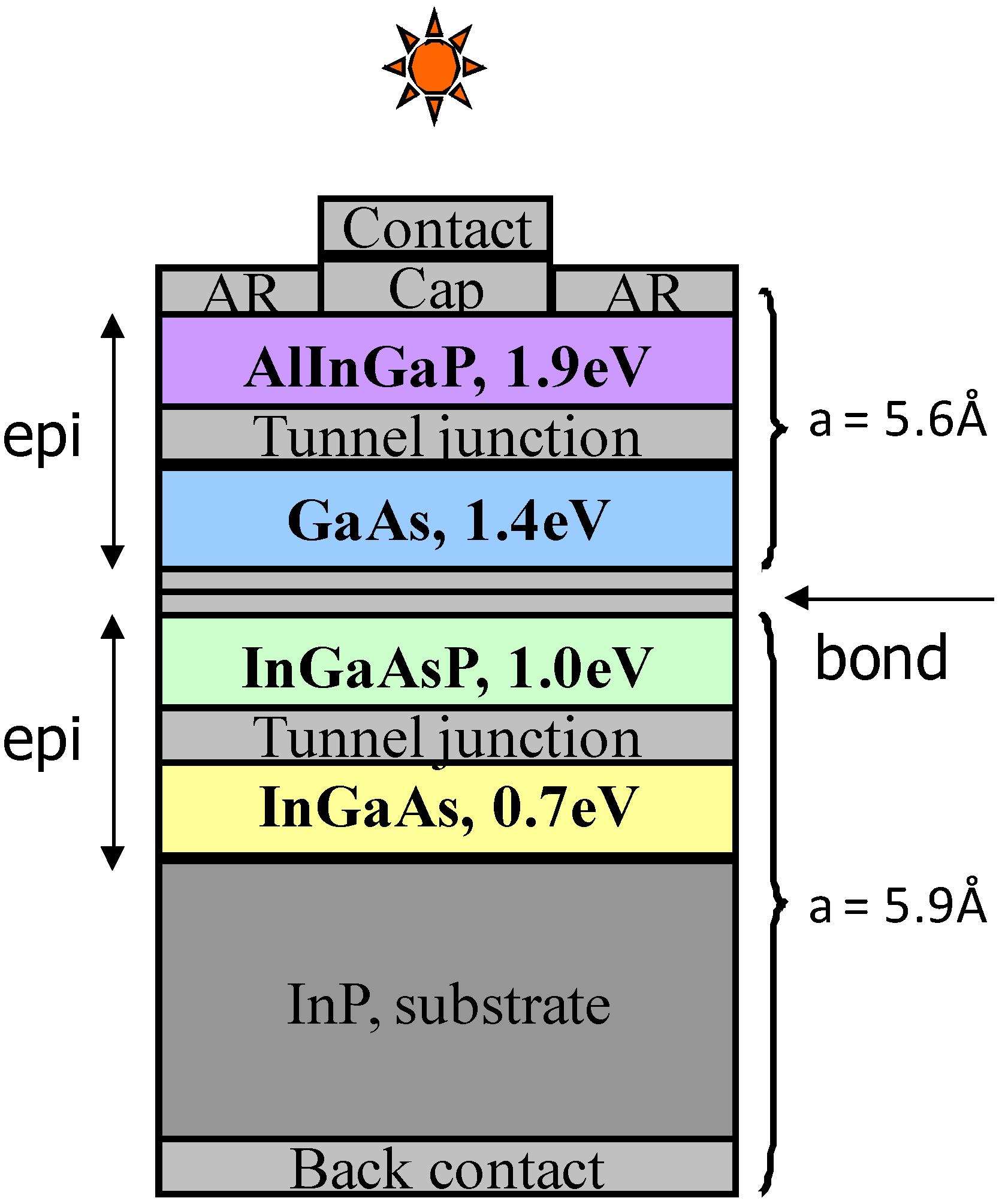
  60. Tanabe, K.; Morral, A.F.I.; Atwater, H.A.; Aiken, D.J.; Wanlass, M.W. Direct-bonded GaAs/InGaAs tandem solar cell. Appl. Phys. Lett. 2006, 89, 102106. [Google Scholar] [CrossRef]
  61. Zahler, J.M.; Tanabe, K.; Ladous, C.; Pinnington, T.; Newman, F.D.; Atwater, H.A. High efficiency InGaAs solar cells on Si by InP layer transfer. Appl. Phys. Lett. 2007, 91, 012108. [Google Scholar] [CrossRef]
  62. Archer, M.J.; Law, D.C.; Mesropian, S.; Haddad, M.; Fetzer, C.M.; Ackerman, A.C.; Ladous, C.; King, R.R.; Atwater, H.A. GaInP/GaAs dual junction solar cells on Ge/Si epitaxial templates. Appl. Phys. Lett. 2008, 92, 103503. [Google Scholar] [CrossRef]
  63. Nozik, A.J. Quantum dot solar cells. Physica E 2002, 14, 115–120. [Google Scholar] [CrossRef]
  64. Schaller, R.D.; Klimov, V.I. High efficiency carrier multiplication in PbSe nanocrystals: Implications for solar energy conversion. Phys. Rev. Lett. 2004, 92, 186601. [Google Scholar] [CrossRef] [PubMed]
  65. Wolf, M.; Brendel, R.; Werner, J.H.; Queisser, H.J. Solar cell efficiency and carrier multiplication in Si1-xGex alloys. J. Appl. Phys. 1998, 83, 4213–4221. [Google Scholar] [CrossRef]
  66. Ellingson, R.J.; Beard, M.C.; Johnson, J.C.; Yu, P.R.; Micic, O.I.; Nozik, A.J.; Shabaev, A.; Efros, A.L. Highly efficient multiple exciton generation in colloidal PbSe and PbS quantum dots. Nano Lett. 2005, 5, 865–871. [Google Scholar] [CrossRef] [PubMed]
  67. Schaller, R.D.; Sykora, M.; Pietryga, J.M.; Klimov, V.I. Seven excitons at a cost of one: Redefining the limits for conversion efficiency of photons into charge carriers. Nano Lett. 2006, 6, 424–429. [Google Scholar] [CrossRef] [PubMed]
  68. Klimov, V.I. Mechanisms for photogeneration and recombination of multiexcitons in semiconductor nanocrystals: Implications for lasing and solar energy conversion. J. Phys. Chem. B 2006, 110, 16827–16845. [Google Scholar] [CrossRef] [PubMed]
  69. Klimov, V.I. Spectral and dynamical properties of multilexcitons in semiconductor nanocrystals. Ann. Rev. Phys. Chem. 2007, 58, 635–673. [Google Scholar] [CrossRef] [PubMed]
  70. Pijpers, J.J.H.; Hendry, E.; Milder, M.T.W.; Fanciulli, R.; Savolainen, J.; Herek, J.L.; Vanmaekelbergh, D.; Ruhman, S.; Mocatta, D.; Oron, D.; Aharoni, A.; Banin, U.; Bonn, M. Carrier multiplication and its reduction by photodoping in colloidal InAs quantum dots. J. Phys. Chem. C 2007, 111, 4146–4152. [Google Scholar] [CrossRef]
  71. Schaller, R.D.; Pietryga, J.M.; Klimov, V.I. Carrier multiplication in InAs nanocrystal quantum dots with an onset defined by the energy conservation limit. Nano Lett. 2007, 7, 3469–3476. [Google Scholar] [CrossRef] [PubMed]
  72. Beard, M.C.; Knutsen, K.P.; Yu, P.R.; Luther, J.M.; Song, Q.; Metzger, W.K.; Ellingson, R.J.; Nozik, A.J. Multiple exciton generation in colloidal silicon nanocrystals. Nano Lett. 2007, 7, 2506–2512. [Google Scholar] [CrossRef] [PubMed]
  73. Klein, C.A. Bandgap dependence and related features of radiation ionization energies in semiconductors. J. Appl. Phys. 1968, 39, 2029–2038. [Google Scholar] [CrossRef]
  74. Alig, R.C.; Bloom, S. Electron-hole-pair creation energies in semiconductors. Phys. Rev. Lett. 1975, 35, 1522–1525. [Google Scholar] [CrossRef]
  75. Klimov, V.I. Detailed-balance power conversion limits of nanocrystal-quantum-dot solar cells in the presence of carrier multiplication. Appl. Phys. Lett. 2006, 89, 123118. [Google Scholar] [CrossRef]
  76. Hanna, M.C.; Nozik, A.J. Solar conversion efficiency of photovoltaic and photoelectrolysis cells with carrier multiplication absorbers. J. Appl. Phys. 2006, 100, 074510. [Google Scholar] [CrossRef]
  77. Tanabe, K. Enhanced energy conversion efficiencies of solar cells by multiple carrier excitation. Electron. Lett. 2007, 43, 998–999. [Google Scholar] [CrossRef]
  78. Franceschetti, A.; An, J.M.; Zunger, A. Impact ionization can explain carrier multiplication in PbSe quantum dots. Nano Lett. 2006, 6, 2191–2195. [Google Scholar] [CrossRef] [PubMed]
  79. Schaller, R.D.; Agranovich, V.M.; Klimov, V.I. High-efficiency carrier multiplication through direct photogeneration of multi-excitons via virtual single-exciton states. Nat. Phys. 2005, 1, 189–194. [Google Scholar] [CrossRef]
  80. Trinh, M.T.; Houtepen, A.J.; Schins, J.M.; Hanrath, T.; Piris, J.; Knulst, W.; Goossens, A.; Siebbeles, L.D.A. In spite of recent doubts carrier multiplication does occur in PbSe nanocrystals. Nano Lett. 2008, 8, 1713–1718. [Google Scholar] [CrossRef] [PubMed]
  81. Wegh, R.T.; Donker, H.; Oskam, K.D.; Meijerink, A. Visible quantum cutting in LiGdF4:Eu3+ through downconversion. Science 1999, 283, 663–666. [Google Scholar] [CrossRef] [PubMed]
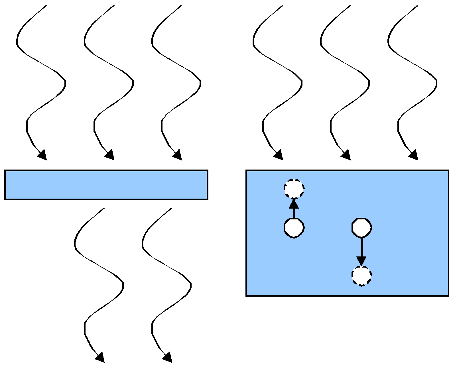
  82. Trupke, T.; Green, M.A.; Wurfel, P. Improving solar cell efficiencies by down-conversion of high-energy photons. J. Appl. Phys. 2002, 92, 1668–1674. [Google Scholar] [CrossRef]
  83. Timmerman, D.; Izeddin, I.; Stallinga, P.; Yassievich, I.N.; Gregorkiewicz, T. Space-separated quantum cutting with silicon nanocrystals for photovoltaic applications. Nat. Photonics 2008, 2, 105–109. [Google Scholar] [CrossRef]
  84. Auzel, F. Upconversion processes in coupled ion systems. J. Lumin. 1990, 45, 341–345. [Google Scholar] [CrossRef]
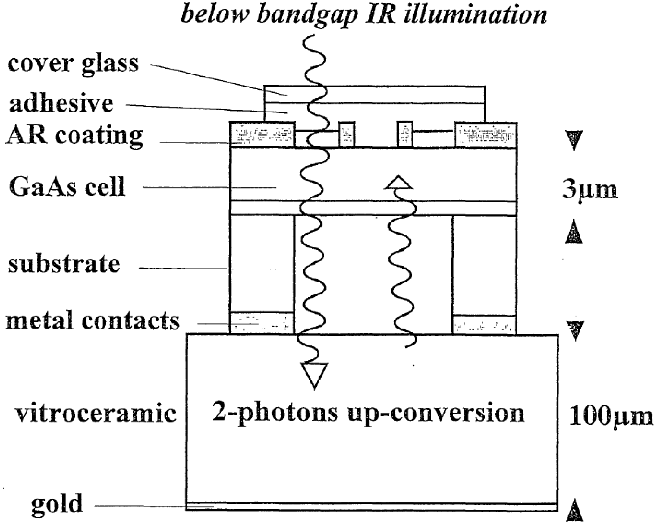
  85. Gibart, P.; Auzel, F.; Guillaume, J.C.; Zahraman, K. Below band-gap IR response of substrate-free GaAs solar cells using two-photon up-conversion. Jpn. J. Appl. Phys. 1996, 35, 4401–4402. [Google Scholar] [CrossRef]
  86. Trupke, T.; Green, M.A.; Wurfel, P. Improving solar cell efficiencies by up-conversion of sub-band-gap light. J. Appl. Phys. 2002, 92, 4117–4122. [Google Scholar] [CrossRef]
  87. Wolf, M. Limitations and possibilities for improvement of photovoltaic solar energy converters 1. Considerations for earth’s surface operation. Proc. IRE 1960, 48, 1246–1263. [Google Scholar] [CrossRef]
  88. Beaucarne, G.; Brown, A.S.; Keevers, M.J.; Corkish, R.; Green, M.A. The impurity photovoltaic (IPV) effect in wide-bandgap semiconductors: an opportunity for very-high-efficiency solar cells? Prog. Photovoltaics Res. Appl. 2002, 10, 345–353. [Google Scholar] [CrossRef]
  89. Barnham, K.W.J.; Duggan, G. A new approach to high-efficiency multi-band-gap solar-cells. J. Appl. Phys. 1990, 67, 3490–3493. [Google Scholar] [CrossRef]
  90. Paxman, M.; Nelson, J.; Braun, B.; Connolly, J.; Barnham, K.W.J.; Foxon, C.T.; Roberts, J.S. Modeling the spectral response of the quantum-well solar-cell. J. Appl. Phys. 1993, 74, 614–621. [Google Scholar] [CrossRef]
  91. Aroutiounian, V.; Petrosyan, S.; Khachatryan, A.; Touryan, K. Quantum dot solar cells. J. Appl. Phys. 2001, 89, 2268–2271. [Google Scholar] [CrossRef]
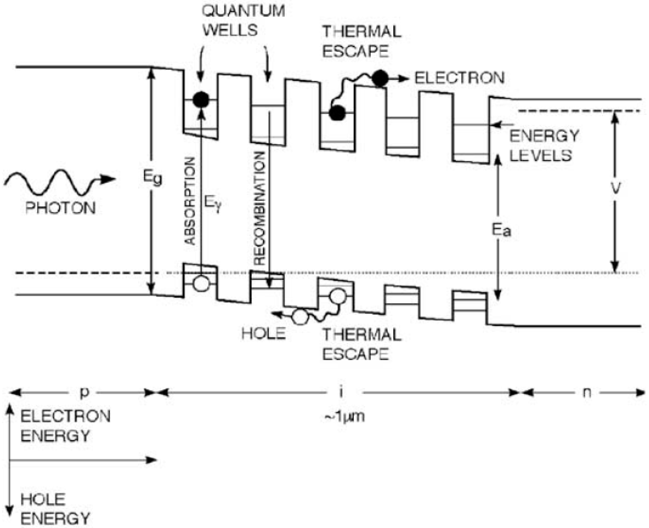
  92. Barnham, K.W.J.; Ballard, I.; Connolly, J.P.; Ekins-Daukes, N.J.; Kluftinger, B.G.; Nelson, J.; Rohr, C. Quantum well solar cells. Physica E 2002, 14, 27–36. [Google Scholar] [CrossRef]
  93. Luque, A.; Marti, A. Increasing the efficiency of ideal solar cells by photon induced transitions at intermediate levels. Phys. Rev. Lett. 1997, 78, 5014–5017. [Google Scholar] [CrossRef]
  94. Chen, C.K.; Decastro, A.R.B.; Shen, Y.R. Surface-enhanced 2nd-harmonic generation. Phys. Rev. Lett. 1981, 46, 145–148. [Google Scholar] [CrossRef]
  95. Wokaun, A.; Bergman, J.G.; Heritage, J.P.; Glass, A.M.; Liao, P.F.; Olson, D.H. Surface 2nd-harmonic generation from metal island films and microlithographic structures. Phys. Rev. B 1981, 24, 849–856. [Google Scholar] [CrossRef]
  96. Garcia-Vidal, F.J.; Pendry, J.B. Collective theory for surface enhanced Raman scattering. Phys. Rev. Lett. 1996, 77, 1163–1166. [Google Scholar] [CrossRef] [PubMed]
  97. Cao, Y.W.C.; Jin, R.C.; Mirkin, C.A. Nanoparticles with Raman spectroscopic fingerprints for DNA and RNA detection. Science 2002, 297, 1536–1540. [Google Scholar] [CrossRef] [PubMed]
  98. Fritzsche, W.; Taton, T.A. Metal nanoparticles as labels for heterogeneous, chip-based DNA detection. Nanotechnology 2003, 14, R63–R73. [Google Scholar] [CrossRef] [PubMed]
  99. Wenseleers, W.; Stellacci, F.; Meyer-Friedrichsen, T.; Mangel, T.; Bauer, C.A.; Pond, S.J.K.; Marder, S.R.; Perry, J.W. Five orders-of-magnitude enhancement of two-photon absorption for dyes on silver nanoparticle fractal clusters. J. Phys. Chem. B 2002, 106, 6853–6863. [Google Scholar] [CrossRef]
  100. Yin, X.B.; Fang, N.; Zhang, X.; Martini, I.B.; Schwartz, B.J. Near-field two-photon nanolithography using an apertureless optical probe. Appl. Phys. Lett. 2002, 81, 3663–3665. [Google Scholar] [CrossRef]
  101. Maier, S.A.; Atwater, H.A. Plasmonics: Localization and guiding of electromagnetic energy in metal/dielectric structures. J. Appl. Phys. 2005, 98, 011101. [Google Scholar] [CrossRef]
  102. Atwater, H.A. The promise of plasmonics. Sci. Am. 2007, 296, 56–63. [Google Scholar] [CrossRef] [PubMed]
  103. Quinten, M.; Leitner, A.; Krenn, J.R.; Aussenegg, F.R. Electromagnetic energy transport via linear chains of silver nanoparticles. Opt. Lett. 1998, 23, 1331–1333. [Google Scholar] [CrossRef] [PubMed]
  104. Maier, S.A.; Kik, P.G.; Atwater, H.A.; Meltzer, S.; Harel, E.; Koel, B.E.; Requicha, A.A.G. Local detection of electromagnetic energy transport below the diffraction limit in metal nanoparticle plasmon waveguides. Nat. Mater. 2003, 2, 229–232. [Google Scholar] [CrossRef] [PubMed]
  105. Maier, S.A.; Brongersma, M.L.; Atwater, H.A. Electromagnetic energy transport along Yagi arrays. Mater. Sci. Eng. C 2002, 19, 291–294. [Google Scholar] [CrossRef]
  106. Barnes, W.L.; Dereux, A.; Ebbesen, T.W. Surface plasmon subwavelength optics. Nature 2003, 424, 824–830. [Google Scholar] [CrossRef] [PubMed]
  107. Dobrzynski, L.; Akjouj, A.; Djafari-Rouhani, B.; Vasseur, J.O.; Bouazaoui, M.; Vilcot, J.P.; Al Wahsh, H.; Zielinski, P.; Vigneron, J.P. Simple nanometric plasmon multiplexer. Phys. Rev. E 2004, 69, 035601. [Google Scholar] [CrossRef]
  108. Pacifici, D.; Lezec, H.J.; Atwater, H.A. All-optical modulation by plasmonic excitation of CdSe quantum dots. Nat. Photonics 2007, 1, 402–406. [Google Scholar] [CrossRef]
  109. Stuart, H.R.; Hall, D.G. Absorption enhancement in silicon-on-insulator waveguides using metal island films. Appl. Phys. Lett. 1996, 69, 2327–2329. [Google Scholar] [CrossRef]
  110. Stuart, H.R.; Hall, D.G. Island size effects in nanoparticle-enhanced photodetectors. Appl. Phys. Lett. 1998, 73, 3815–3817. [Google Scholar] [CrossRef]
  111. Schaadt, D.M.; Feng, B.; Yu, E.T. Enhanced semiconductor optical absorption via surface plasmon excitation in metal nanoparticles. Appl. Phys. Lett. 2005, 86, 063106. [Google Scholar] [CrossRef]
  112. Pillai, S.; Catchpole, K.R.; Trupke, T.; Zhang, G.; Zhao, J.; Green, M.A. Enhanced emission from Si-based light-emitting diodes using surface plasmons. Appl. Phys. Lett. 2006, 88, 161102. [Google Scholar] [CrossRef]
  113. Derkacs, D.; Lim, S.H.; Matheu, P.; Mar, W.; Yu, E.T. Improved performance of amorphous silicon solar cells via scattering from surface plasmon polaritons in nearby metallic nanoparticles. Appl. Phys. Lett. 2006, 89, 093103. [Google Scholar] [CrossRef]
  114. Catchpole, K.R.; Pillai, S. Absorption enhancement due to scattering by dipoles into silicon waveguides. J. Appl. Phys. 2006, 100, 044504. [Google Scholar] [CrossRef]
  115. Pillai, S.; Catchpole, K.R.; Trupke, T.; Green, M.A. Surface plasmon enhanced silicon solar cells. J. Appl. Phys. 2007, 101, 093105. [Google Scholar] [CrossRef]
  116. Ihara, M.; Tanaka, K.; Sakaki, K.; Honma, I.; Yamada, K. Enhancement of the absorption coefficient of cis-(NCS)(2) bis(2,2'-bipyridyl-4,4'-dicarboxylate)ruthenium(II) dye in dye-sensitized solar cells by a silver island film. J. Phys. Chem. B 1997, 101, 5153–5157. [Google Scholar] [CrossRef]
  117. Wen, C.; Ishikawa, K.; Kishima, M.; Yamada, K. Effects of silver particles on the photovoltaic properties of dye-sensitized TiO2 thin films. Sol. Energy Mater. Sol. Cells 2000, 61, 339–351. [Google Scholar] [CrossRef]
  118. Rand, B.P.; Peumans, P.; Forrest, S.R. Long-range absorption enhancement in organic tandem thin-film solar cells containing silver nanoclusters. J. Appl. Phys. 2004, 96, 7519–7526. [Google Scholar] [CrossRef]
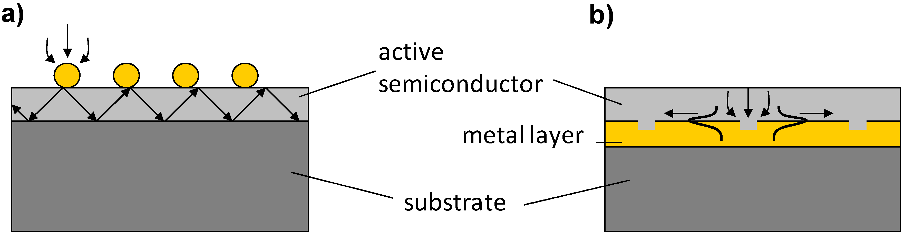
  119. Tanabe, K.; Nakayama, K.; Atwater, H.A. Plasmon-enhanced absorption and photocurrent in ultrathin GaAs solar cells with metallic nanostructures. In Proceedings of the 33rd IEEE Photovoltaic Specialists Conference, San Diego, CA, USA, May 2008; p. 129.
  120. Nakayama, K.; Tanabe, K.; Atwater, H.A. Plasmonic nanoparticle enhanced light absorption in GaAs solar cells. Appl. Phys. Lett. 2008, 93, 121904. [Google Scholar] [CrossRef]
  121. Chang, T.H.; Wu, P.H.; Chen, S.H.; Chan, C.H.; Lee, C.C.; Chen, C.C.; Su, Y.K. Efficiency enhancement in GaAs solar cells using self-assembled microspheres. Opt. Express 2009, 17, 6519–6524. [Google Scholar] [CrossRef] [PubMed]
  122. Lezec, H.J.; Thio, T. Diffracted evanescent wave model for enhanced and suppressed optical transmission through subwavelength hole arrays. Opt. Express 2004, 12, 3629–3651. [Google Scholar] [CrossRef] [PubMed]
  123. Gay, G.; Alloschery, O.; De Lesegno, B.V.; O’Dwyer, C.; Weiner, J.; Lezec, H.J. The optical response of nanostructured surfaces and the composite diffracted evanescent wave model. Nat. Phys. 2006, 2, 262–267. [Google Scholar] [CrossRef]
  124. Chen, L.; Robinson, J.T.; Lipson, M. Role of radiation and surface plasmon polaritons in the optical interactions between a nano-slit and a nano-groove on a metal surface. Opt. Express 2006, 14, 12629–12636. [Google Scholar] [CrossRef] [PubMed]
  125. Ferry, V.E.; Sweatlock, L.A.; Pacifici, D.; Atwater, H.A. Plasmonic nanostructure design for efficient light coupling into solar cells. Nano Lett. 2008, 8, 4391–4397. [Google Scholar] [CrossRef] [PubMed]
  126. Tanabe, K. Low-cost high-efficiency solar cells with wafer bonding and plasmonic technologies. Ph.D. thesis, California Institute of Technology, Pasadena, CA, USA, 2008. [Google Scholar]

