1. Introduction
The electronic power transformer (EPT), usually referred to as power electronic transformer (PET) or solid state transformer (SST), is a new sort of power transformer, which is based on power electronic converters. The concept of EPT was first mentioned in 1970s [
1], and it has attracted more and more attention in recent decades with the development of power electronic technology. In fact, a significant advantage of EPT is that the magnitude and phase angle of voltages in both the primary side and the secondary side of EPT can be controlled in real-time through power electronic converters to achieve flexible regulation of the current and power. As a result, EPT can be regarded as a power transformer with the functions of a FACTS (Flexible Alternative Current Transmission System) or DFACTS (Distribution Flexible Alternative Current Transmission System) device. It can be applied in generation, transmission and distribution systems. A unique characteristic of EPT is that the output voltage and frequency are adjustable; hence they can be set up for all kinds of applications. This means that EPT can offer a customized power supply with a particular voltage level and particular frequency without additional power transformers and frequency conversion equipment [
2].
Due to the fact that an EPT consists of power electronic converters, the reliability of EPT which is always of special significance for the electric power system is dependent on those power electronic converters and power switches. Hence the fault characteristics, fault detection and protection of those power electronic converters and power switches are of great importance for EPT, whose failure could result in damage to the whole power system and loss to end user.
Faults occurring in power switches can be generally classified into short-circuit and open-circuit faults [
3]. In the short-circuit fault, the fault detection and protection should be very fast and based on a hardware circuit as time between fault initiation and failure is very short [
4,
5]. Therefore, the protection circuits against the short-circuit fault of power switches have become a standard part integrated in the gate driver for practical industrial applications. Meanwhile, the open-circuit fault has not received so much attention yet, in spite of the fact that some methods were proposed for the diagnosis of the open-circuit fault in several power converter topologies and electric machines [
6,
7,
8,
9,
10,
11,
12,
13,
14,
15,
16,
17,
18,
19,
20,
21].
The open-circuit fault may be caused by the lifting of the bonding wires due to the thermal cycling, a driver failure, or a short-circuit fault-induced rupture [
6,
7,
8,
9,
10,
11,
12]. In comparison with the short-circuit fault, the open-circuit fault will not cause the immediate shut down of the whole system, and the converter can still work in an abnormal but steady situation. Moreover, the abnormal state resulting from an open-circuit fault can lead to overstresses on the healthy switches as well as pulsating currents. This can in turn lead to failures of other components.
There have been many researches on the configuration design for EPT [
22,
23,
24,
25] and many literatures have also been studying the EPT applications in electric power system [
26,
27,
28,
29,
30] in the past decade. Some researchers have published technical papers to address the power switch fault diagnosis problem for inverters and converters [
6,
7,
8,
9,
10,
11,
12], in which some of the studies are for inverter motor drive system [
7,
8] and the others are for matrix converters [
9,
10,
11,
12]. However, little effort has been undertaken on analyzing the issues of fault detection, fault characteristics and protection of EPTs. A hierarchical section protection based on EPT for the Future Renewable Electric Energy Delivery and Management (FREEDM) system is proposed in [
31,
32]. Although the protection method is more appropriate than the conventional differential protection scheme, it only focuses on the whole micro-grid system rather than the EPT device. So far, there are no studies conducted specially for the protection of EPTs based on their power switches.
In this paper, the fault characteristics based on the power switches of EPT are proposed for fault detection and EPT protection.
Section 2 gives the topology and operational principles of the EPT, and
Section 3 gives the basic control scheme of the EPT. The possible faults of EPT power switches are systematically analyzed and summarized in
Section 4. In
Section 5, the analysis of the possible faults is verified and further discussed with simulation in Saber. Based on the simulation results, the protection design is discussed in
Section 6. Conclusions are given in
Section 7.
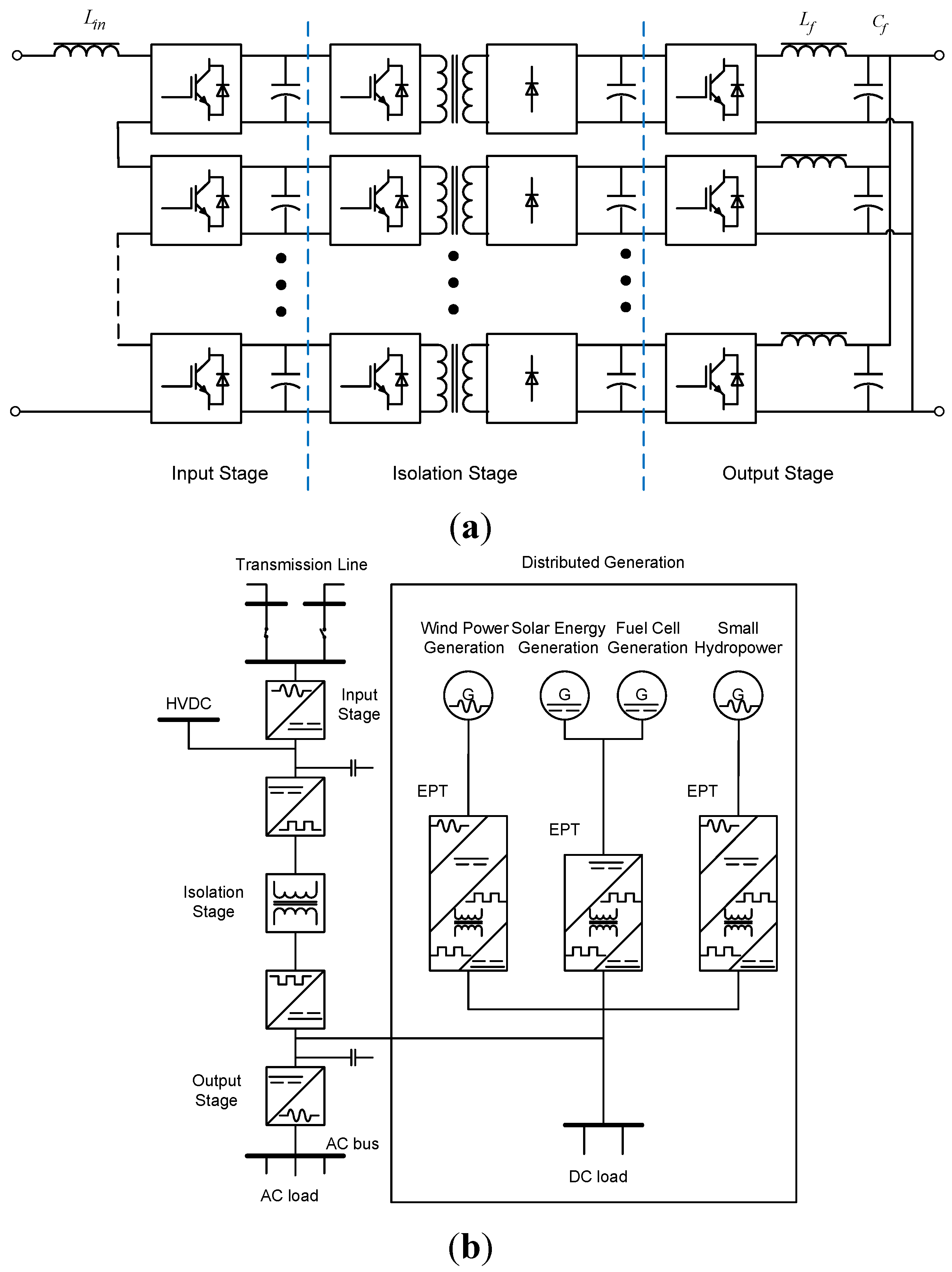
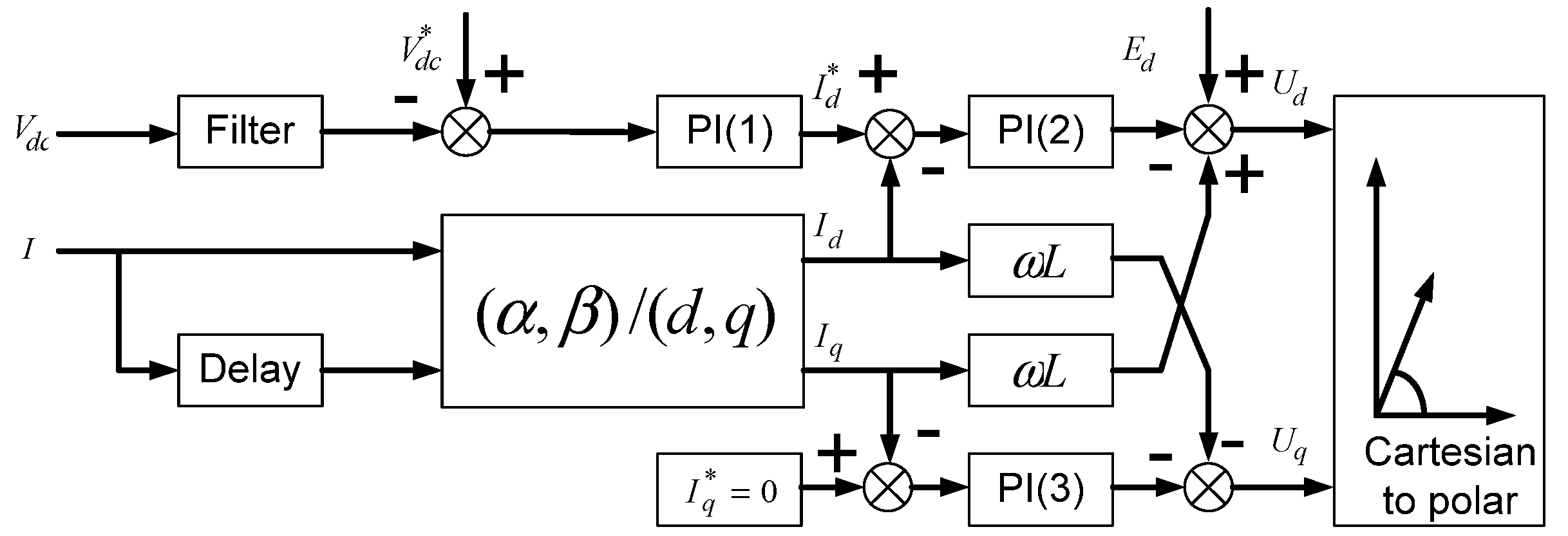
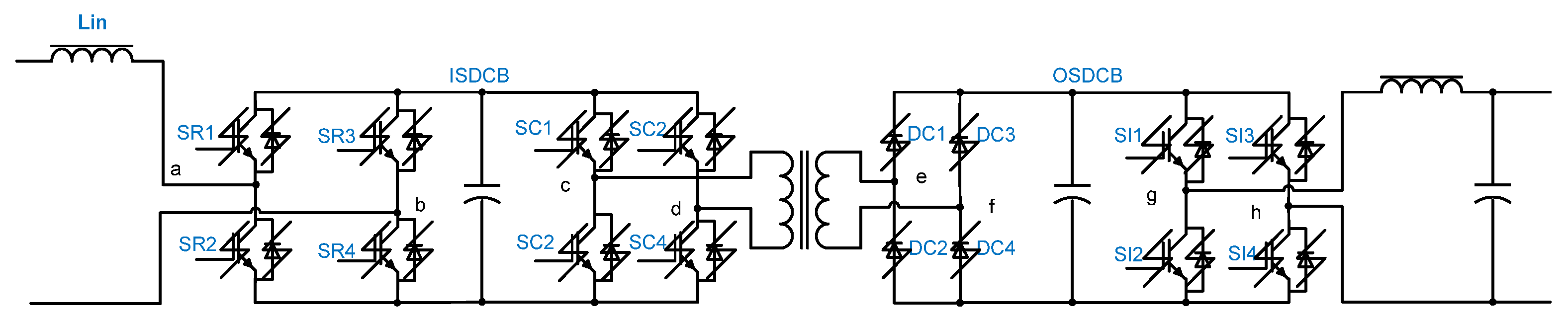
2. Configuration and Operation Principle of D-EPT
The proposed Distribution Electronic Power Transformer (D-EPT) is designed as a 3-phase and 4-wire transformer, and the basic schematic of proposed D-EPT is shown in
Figure 1a. As can be seen from
Figure 1a, the proposed D-EPT is composed of three main stages: an input stage, an isolation stage and an output stage.
Figure 1.
(a) Basic schematic of proposed D-EPT and (b) substation based on EPT.
Figure 1.
(a) Basic schematic of proposed D-EPT and (b) substation based on EPT.
The input stage has multiple H-bridge rectifiers connected in cascade, which convert the input AC voltage to the DC voltages in multiple Input Stage DC buses.
The isolation stage consists of a front-end H-bridge, a High Frequency Isolation Transformer (HFIT) and a diode bridge. The DC voltage from each Input Stage DC Bus is modulated to a high frequency AC wave by a front-end H-bridge chopper, and then the high voltage and high frequency square wave is transformed through a HFIT to the low voltage high frequency square wave on the secondary side of the HFIT. The low voltage square wave is rectified as DC voltage by a diode bridge at the end of isolation stage. In other words, the isolation stage acts like an isolated DC-DC converter.
The output stage has multiple H-bridge inverters connected in parallel, which invert the DC voltage of the Output Stage DC Bus (OSDCB) to an AC sinusoidal voltage.
Figure 1b shows the EPT-based substation which can manage both AC and DC sources; hence the transmission system can connect distributed generation which includes wind power, solar energy and hydro-power. It can be seen from the block diagram that EPT has both AC links and DC links, which would reduce the room and cost of the substation by connecting them in a same substation.
5. Simulation Results
Simulation is performed on the Saber simulation platform (The Synopsys, Mountain View, CA, USA). An EPT shown in
Figure 1a boosts 5774 V input voltage (line voltage 10 kV) to 9000 V DC voltage. The input stage has four cascaded H-bridges, with DC bus voltages of 2250 V each. The isolation stage transforms the ISDCB voltage (2250 V) to OSDCB voltage (375 V), then inverts it to a 230 V (line voltage 400 V) load voltage at the output stage. The input inductor is 30 mH, and the ISDCB capacitor and OSDCB capacitor of one module are 3 mF and 22.4 mF, respectively. With a 230 V output voltage, the load resistor is 2 ohm, hence the output power for single phase and three phase are 26.45 kW and 79.35 kW. The simulation results are summarized in
Table 1, where the abbreviations “UV”, “OV” “OC” and “UB” are used to indicate the under voltage, over voltage, over current, and output currents unbalance, respectively. The faults are generated by a timer which is set to be 0.8 s in the simulation, and the failure IGBTs and diodes are selected as same as in
Section 3 in order to verify the analysis above. During the simulation, the selected failure IGBT will work normally from 0 to 0.8 s, and then set to be open or shorted after 0.8 s according to the timer.
Table 1.
Fault case study with power switches to D-EPT.
Table 1.
Fault case study with power switches to D-EPT.
| Input Stage | A1 | A2 | B1 | Isolation Stage | C1 | C2 | D1 | E1 | F1 | Output Stage | G1 | H1 |
|---|
| Input PF | <0.99 | <0.99 | <0.99 | Input PF | 0.99 | 0.99 | <0.99 | 0.99 | <0.99 | Input PF | 0.99 | <0.99 |
| I_in | | | OC | I_in | | | OC | | OC | I_in | | OC |
| ISDC1 | UV | UV | UV | ISDC1 | | | UV | | UV | ISDC1 | | UV |
| ISDC2 | UV | UV | OV | ISDC2 | | | OV | | OV | ISDC2 | | UV |
| ISDC3 | UV | UV | OV | ISDC3 | | | OV | | OV | ISDC3 | | UV |
| ISDC4 | UV | UV | OV | ISDC4 | | | OV | | OV | ISDC4 | | UV |
| OSDC1 | UV | UV | UV | OSDC1 | | | UV | | UV | OSDC1 | | UV |
| OSDC2 | UV | UV | OV | OSDC2 | | | OV | | OV | OSDC2 | | UV |
| OSDC3 | UV | UV | OV | OSDC3 | | | OV | | OV | OSDC3 | | UV |
| OSDC4 | UV | UV | OV | OSDC4 | | | OV | | OV | OSDC4 | | UV |
| SR1 | | OV | OC | SC1 | | | OC | | OC | SI1 | | OC |
| SR2 | | OV | OC | SC2 | | | OC | | | SI2 | | OC |
| SR3 | | | | SC3 | OC | OC | | OC | OC | SI3 | | OC |
| SR4 | | | | SC4 | OC | OC | | OC | | SI4 | | OC |
| | | | | It_1 | | OC | | | OC | Io_1 | UB | UB |
| | | | | It_2 | | | | | | Io_2 | UB | UB |
| | | | | It_3 | | | | | | Io_3 | UB | UB |
| | | | | It_4 | | | | | | Io_4 | UB | UB |
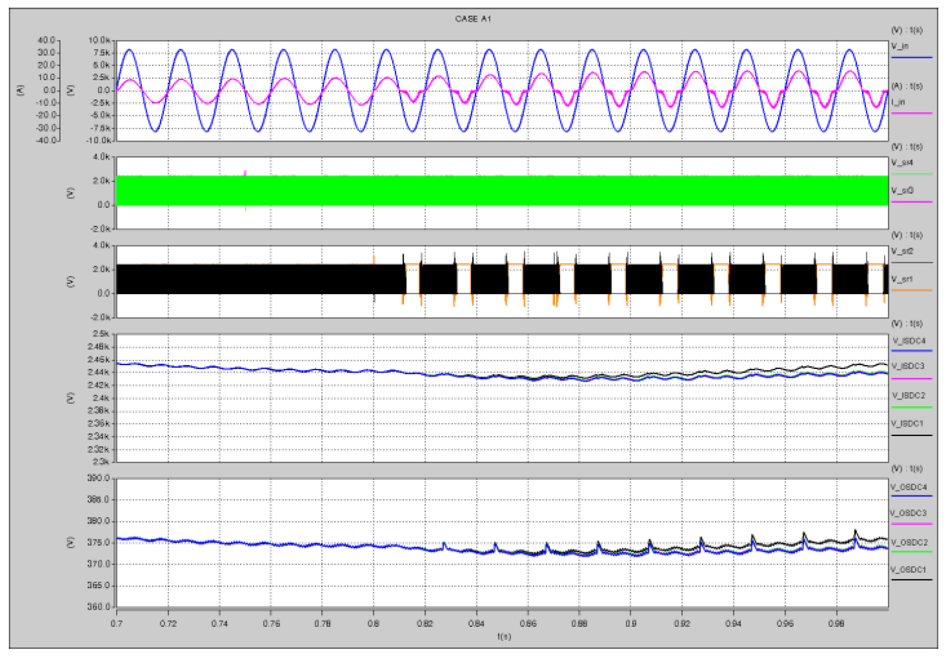
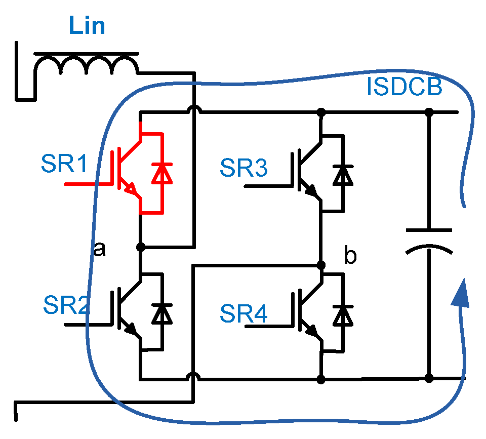
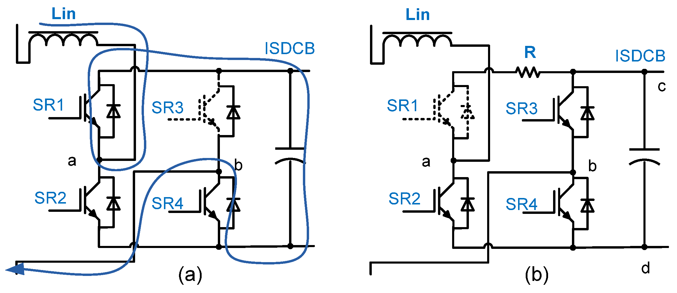
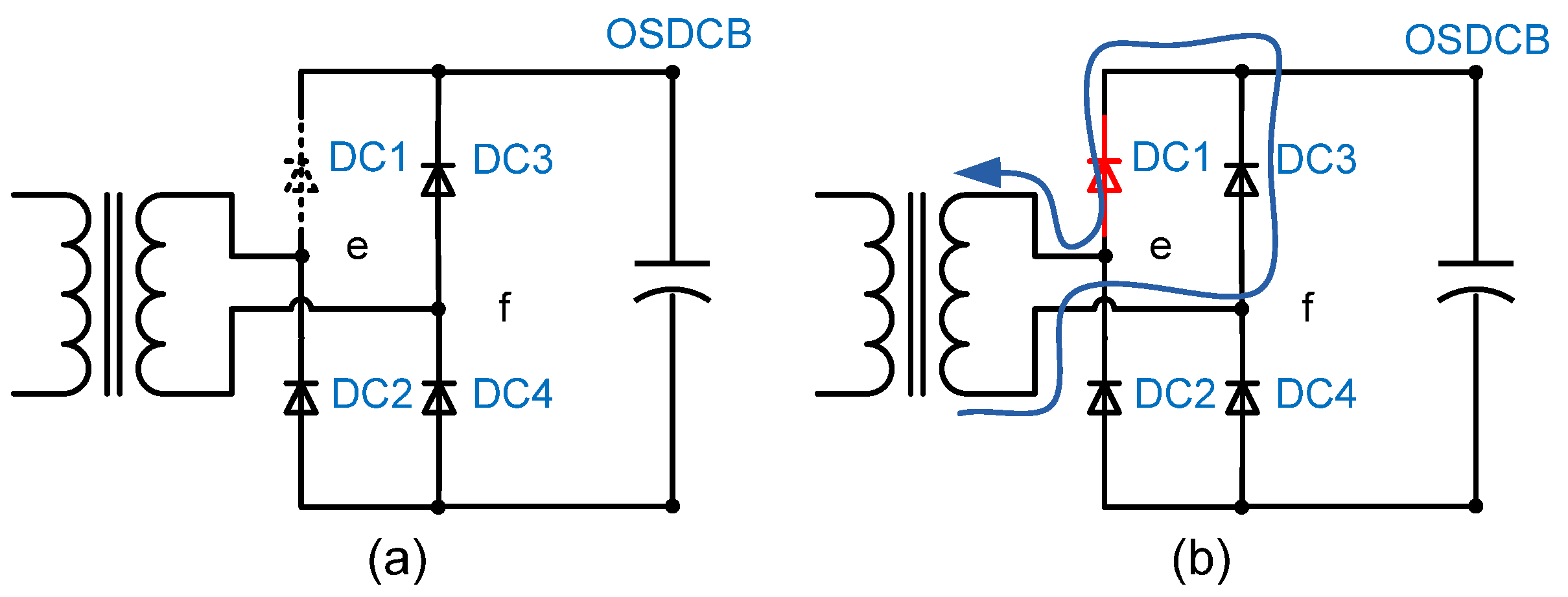
A1. Rectifier IGBT Open-Circuit with Anti-Parallel Diode Normal
Figure 12 shows the A1 fault simulation results of the input voltage (V_in), input current (I_in), the voltage across the IGBTs of the failure H-bridge (V_sr1 to V_sr4), four ISDCB voltages (V_ISDC1 to V_ISDC4) and four OSDCB voltages (V_OSDC1 to V_OSDC4).
It can be observed that the V_ISDC1 and V_OSDC1 increase continuously since the IGBT fault A1 happens on 0.8 s, as well as their ripple voltages. Moreover, I_in is not sinusoidal because it could not follow the V_in due to the fault A1. However, the sum of the DC bus voltage which is the feedback to input stage control scheme remains at 9000 V.
Figure 12.
Simulation results of fault A1.
Figure 12.
Simulation results of fault A1.
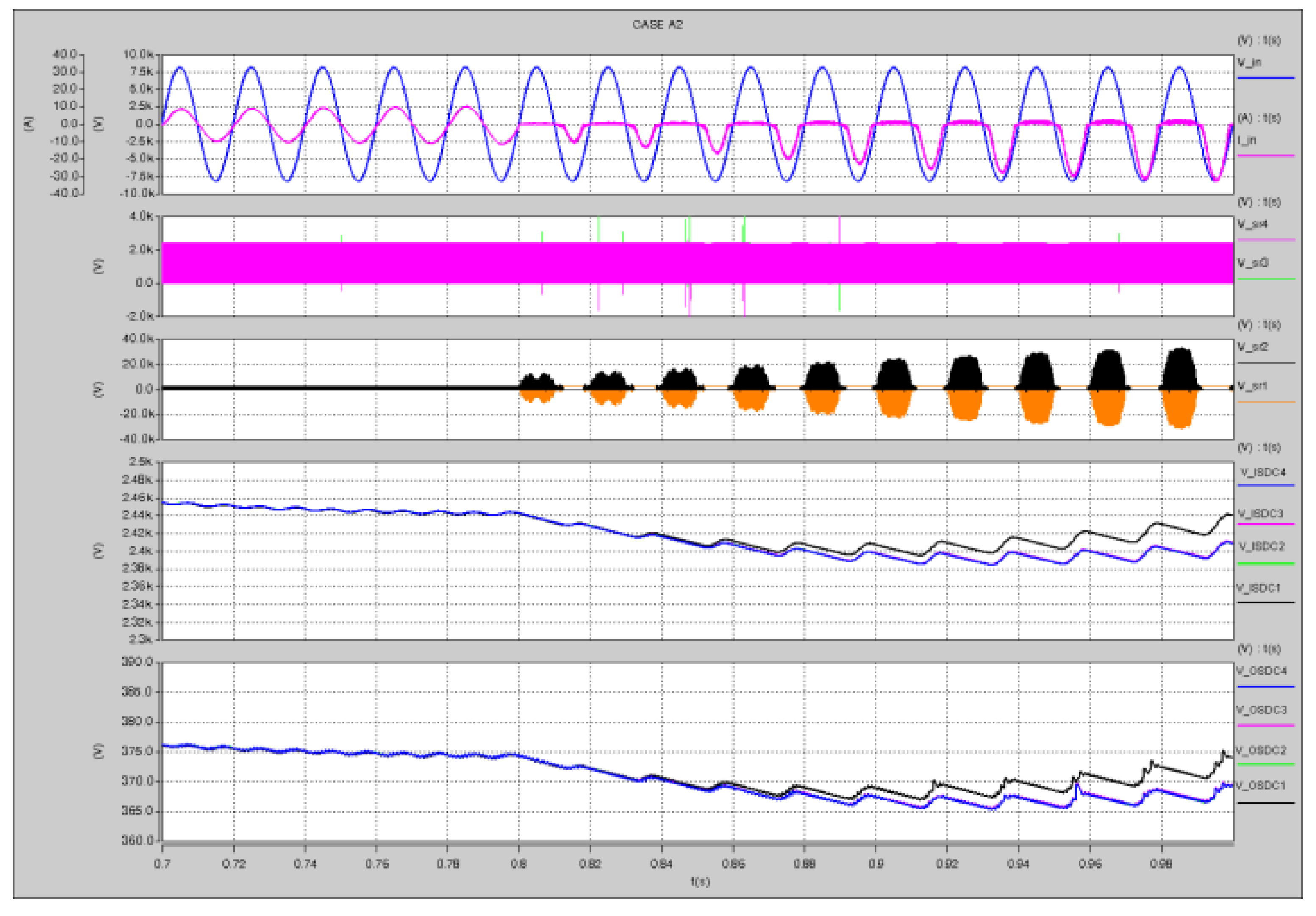
A2. Rectifier IGBT and Its Anti-Parallel Diode both Open-Circuit
Figure 13 shows the A1 fault simulation results of the input voltage, input current, voltage across the IGBTs of the failure H-bridge, 4 ISDCB voltages, and four OSDCB voltages.
Figure 13.
Simulation results of fault A2.
Figure 13.
Simulation results of fault A2.
It can be seen that V_sr1 and V_sr2 are up to 50 kV and −50 kV for the maximum, which are supposed to be 2450 V such as V_sr3 and V_sr4. Hence it will cause over voltage on SR1 and SR2. At the same time, I_in is blocked at the positive half cycle of the source voltage; hence it will be distorted from V_in, which is also shown in
Figure 12. V_ISDC1 and V_OSDC1 keep on increasing after the fault happens, as well as the ripple voltages, which will cause over voltage on the ISDCB and OSDCB capacitors.
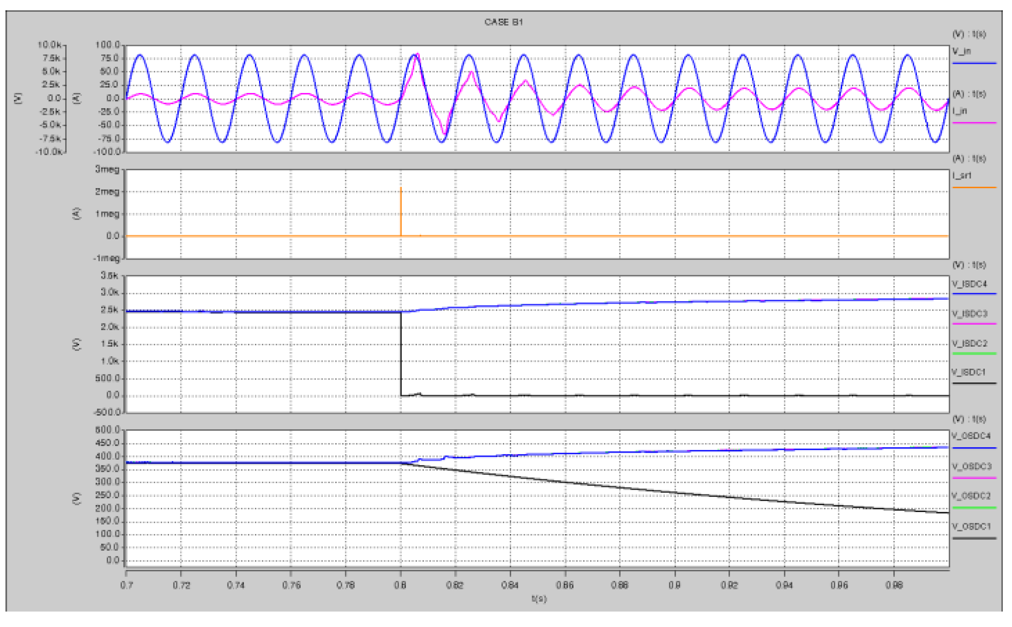
B1. Rectifier IGBT Short-Circuit with Anti-Parallel Diode Normal
Figure 14 shows the B1 fault simulation results of the input voltage, input current, the currents through the IGBTs SR1 (I_sr1), four ISDCB voltages and four OSDCB voltages. It can be seen from
Figure 14 that the current I_sr1 through SR1 at the IGBT failure moment 0.8 s are almost 1 MA, which is because the ISDCB capacitor of the failure H-bridge is shorted by SR2 and shorted SR1. Meanwhile, I_in rises rapidly with its peak value approximately 400 A. Due to the short-circuit fault, V_ISDC1 decreases to 0 V immediately, which will cause ISDCB under voltage. Moreover, V_OSDC1 decreases rapidly as well, as no current will charge the OSDCB capacitor.
Figure 14.
Simulation results of fault B1.
Figure 14.
Simulation results of fault B1.
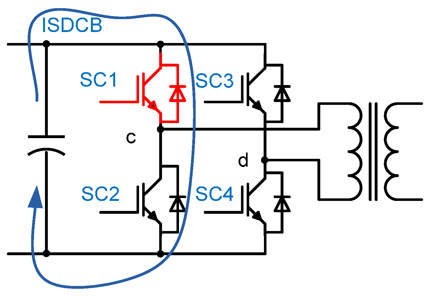
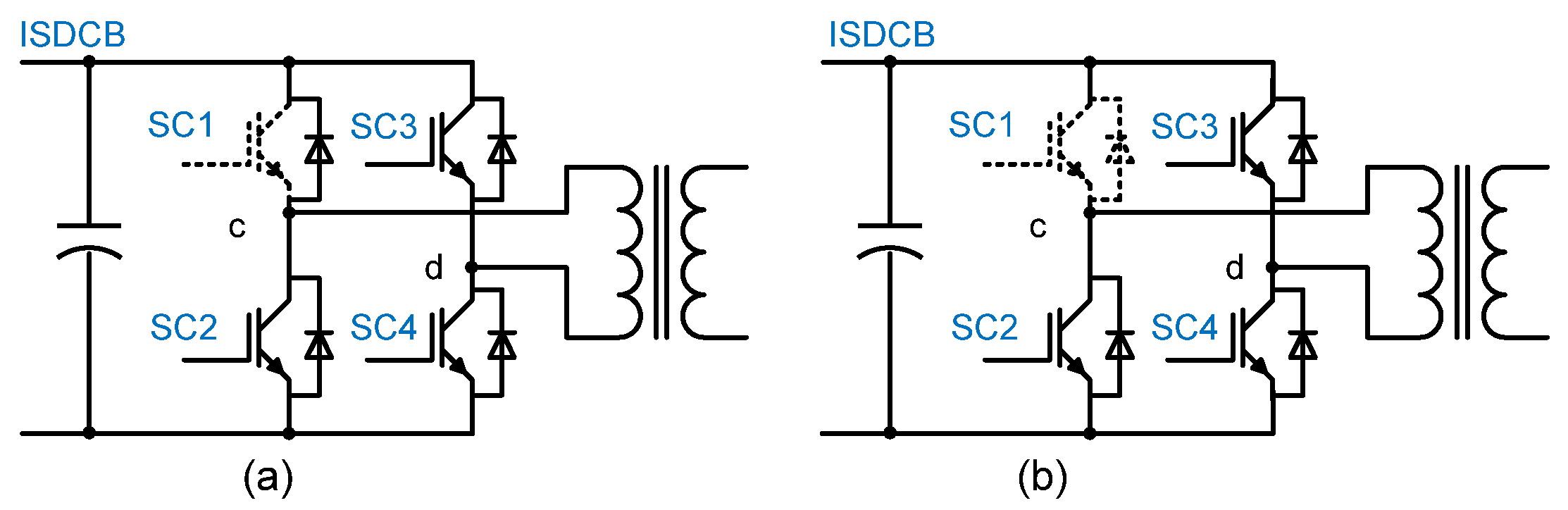
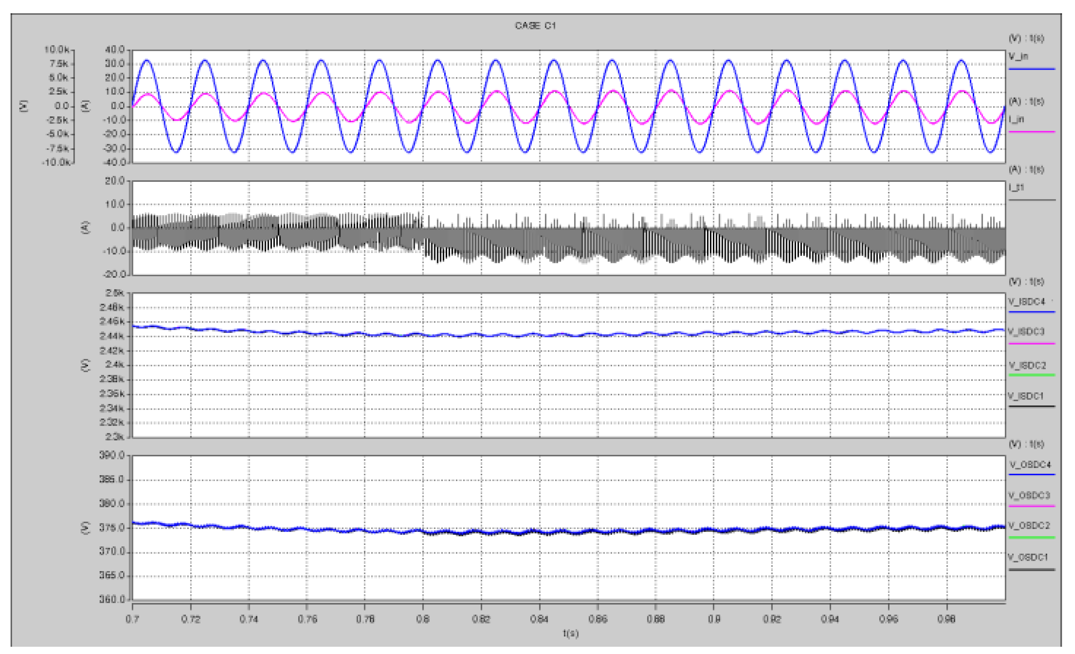
C1. Chopper IGBT Open-Circuit with Anti-Parallel Diode Normal
Figure 15 shows the C1 fault simulation results of the input voltage, input current, the current through the primary side of the HFIT to the failure chopper (I_t1), four ISDCB voltages, and four OSDCB voltages. It can be observed that I_t1 can only flow in one direction since the C1 fault happens at 0.8 s, as the full-bridge chopper becomes a half-bridge chopper. As the HFIT current I_t1 increases as the fault happens, it may cause over current on the IGBT.
Figure 15.
Simulat0ion results of fault C1.
Figure 15.
Simulat0ion results of fault C1.
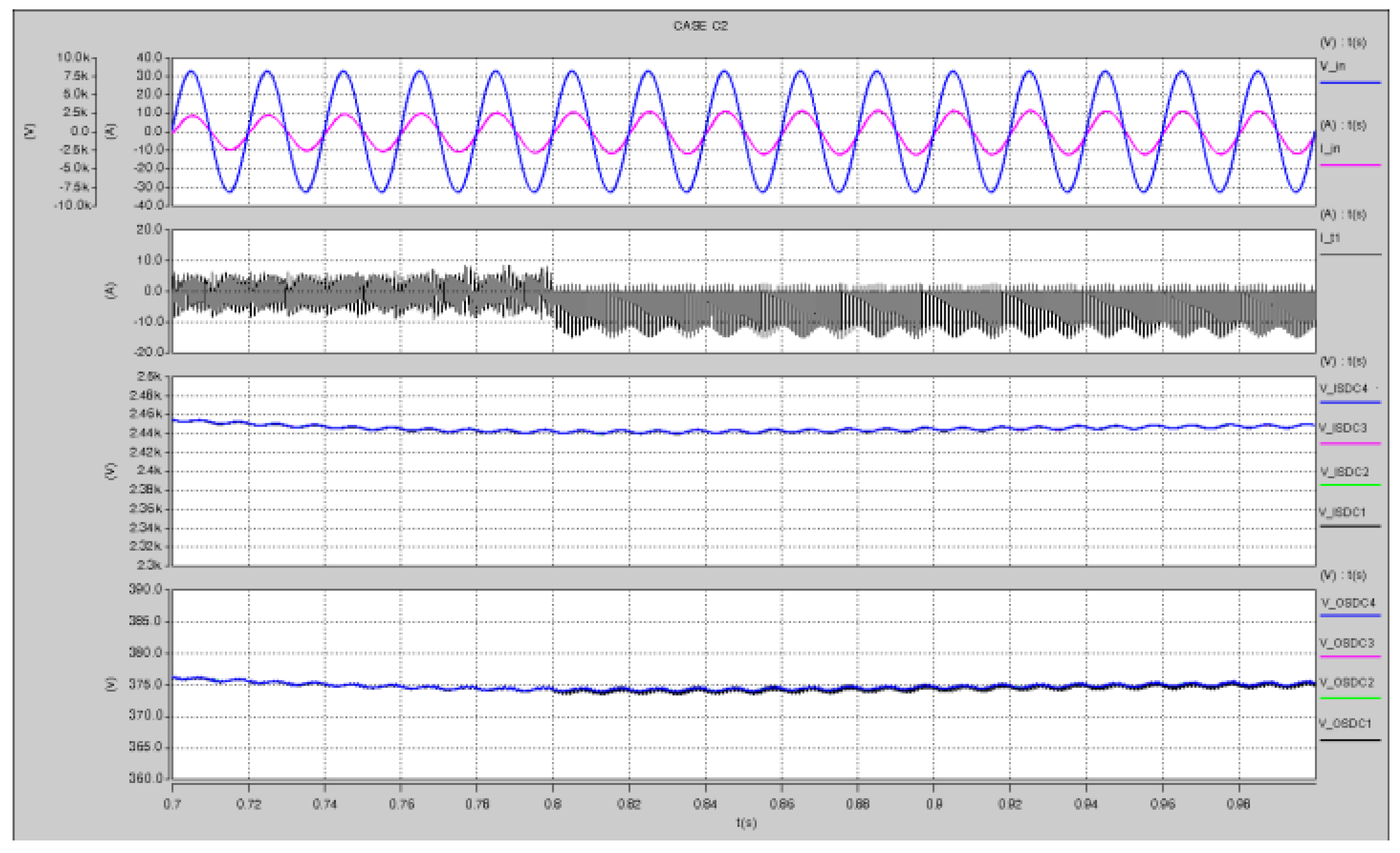
C2. Chopper IGBT and Its Anti-Parallel Diode both Open-Circuit
Figure 16 shows the C2 fault simulation results of the input voltage, the input current, the current through the primary side of the HFIT to the failure chopper, four ISDCB voltages, and four OSDCB voltages. It can be observed that I_t1 can only flow in one direction due to the fact the C2 fault happens at 0.8 s. Unlike the C1 fault, the C2 fault left no path for the magnetizing current to discharge its value when SC1 and its anti-parallel diode are both open-circuit. Hence, I_t1 will continuously increase linearly until it finally saturates the core.
Figure 16.
Simulation results of fault C2.
Figure 16.
Simulation results of fault C2.
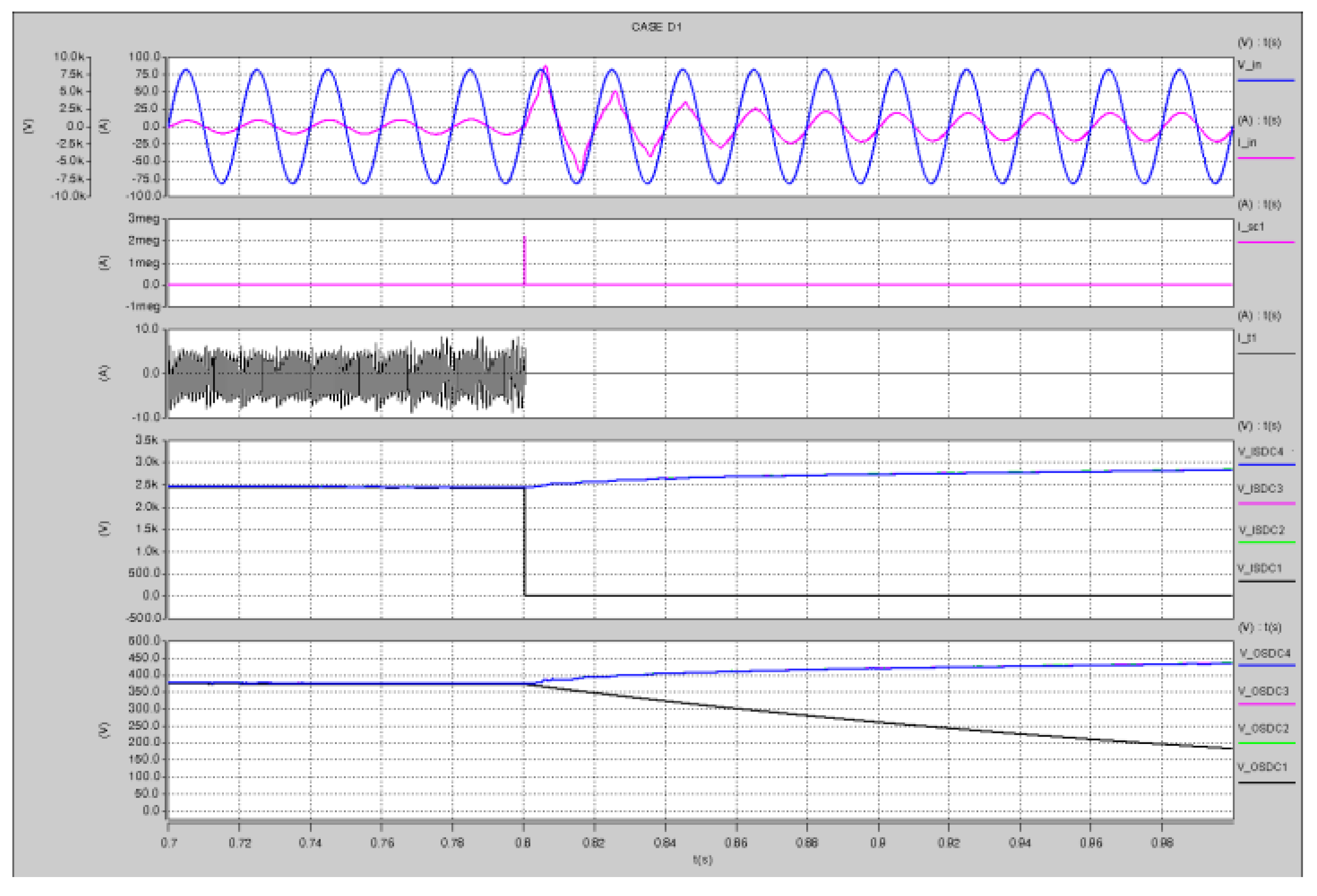
D1. Chopper IGBT Short-Circuit
Figure 17 shows the D1 fault simulation results of the input voltage, input current, the current through the shorted IGBT (I_sc1) and the one through the primary side of the HFIT to the failure chopper H-bridge, four ISDCB voltages and four OSDCB voltages.
It can be observed that I_sc1 is almost 2 MA at the moment of failure at 0.8 s, which is because the ISDCB capacitor of the failure H-bridge is shorted by SC2 and SC1 is shorted. At the same time, the I_in rises rapidly, with its peak value being approximately 75 A. Due to the short-circuit fault, V_ISDC decreases to 0 V when the fault happens, which will reduce I_t1 to 0 A. Moreover, V_OSDC1 will decrease rapidly as well, as no current will charge the OSDCB capacitor due to the short-circuit fault.
Figure 17.
Simulation results of fault D1.
Figure 17.
Simulation results of fault D1.
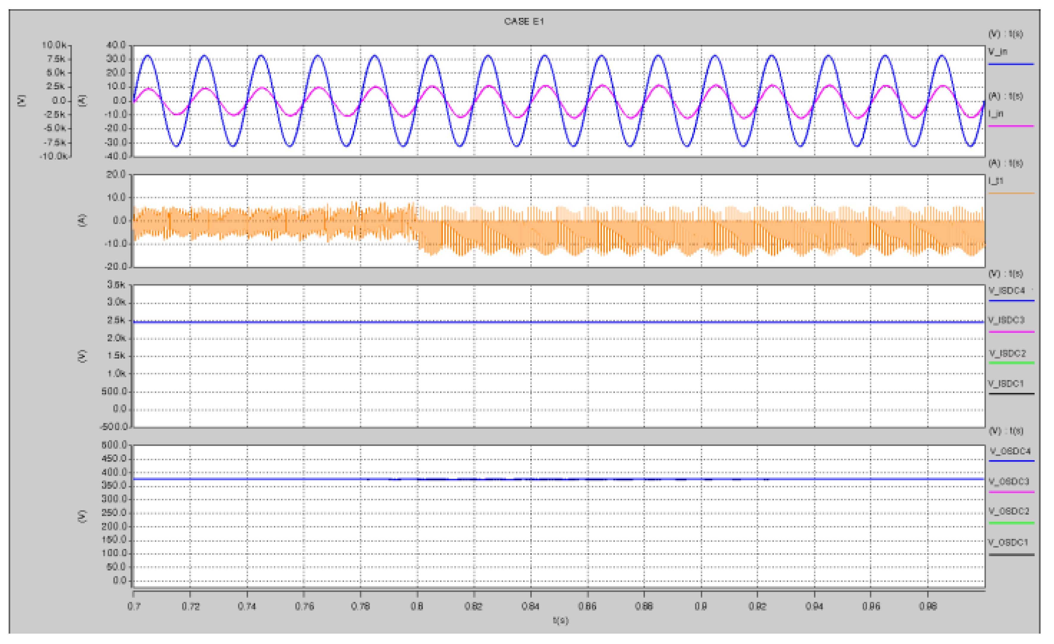
E1. Chopper Rectifier Diode Open-Circuit
Figure 18 shows the E1 fault simulation results of the input voltage, input current, the current through the primary side of the HFIT to the failure chopper, four ISDCB voltages, and four OSDCB voltages. It can be observed that I_t1 can only flow in one direction when the fault E1 happens at 0.8 s. The peak current of the HFIT increases as the full-bridge diode rectifier becomes a half-bridge diode rectifier, which may cause over current on the diode and IGBTs on the primary side of the HFIT.
Figure 18.
Simulation results of fault E1.
Figure 18.
Simulation results of fault E1.
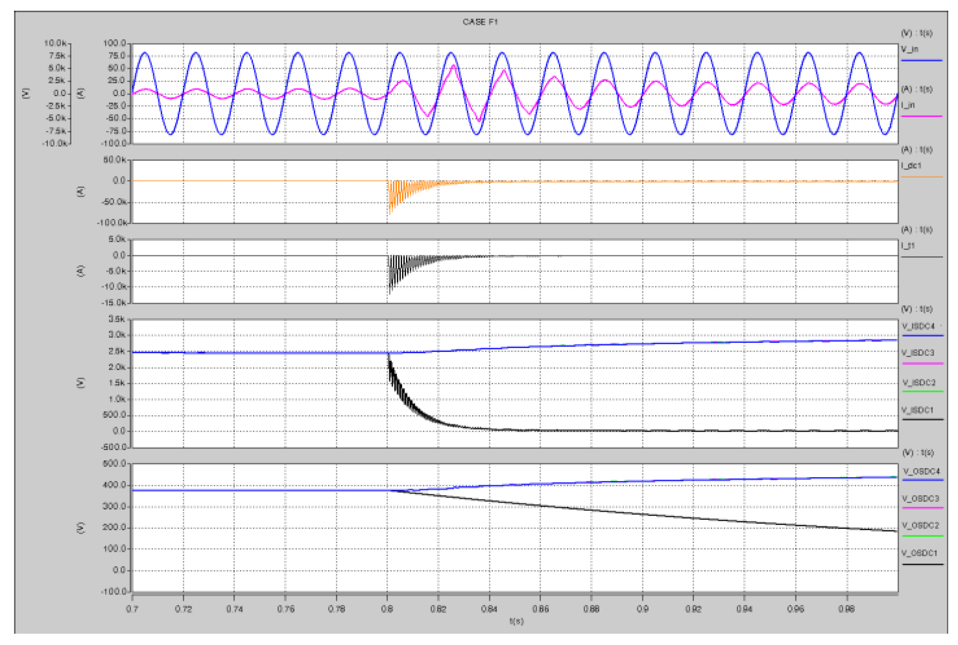
F1. Chopper Rectifier Diode Short-Circuit
Figure 19 shows the F1 fault simulation results of the input voltage, input current, the current through the primary side of the HFIT, and the current through the shorted diode of the failure chopper (I_dc1), four ISDCB voltages and four OSDCB voltages,. It can be observed that I_dc1 and I_t1 at the failure moment are approximately 100 kA and 15 kA, respectively, which are seriously over current. V_ISDC1 decreases to 0 V within 40 ms and V_OSDC1 decreases to 200 V at 1.0 s due to the shorted diode, which are serious under voltages for both DC buses.
Figure 19.
Simulation results of fault F1.
Figure 19.
Simulation results of fault F1.
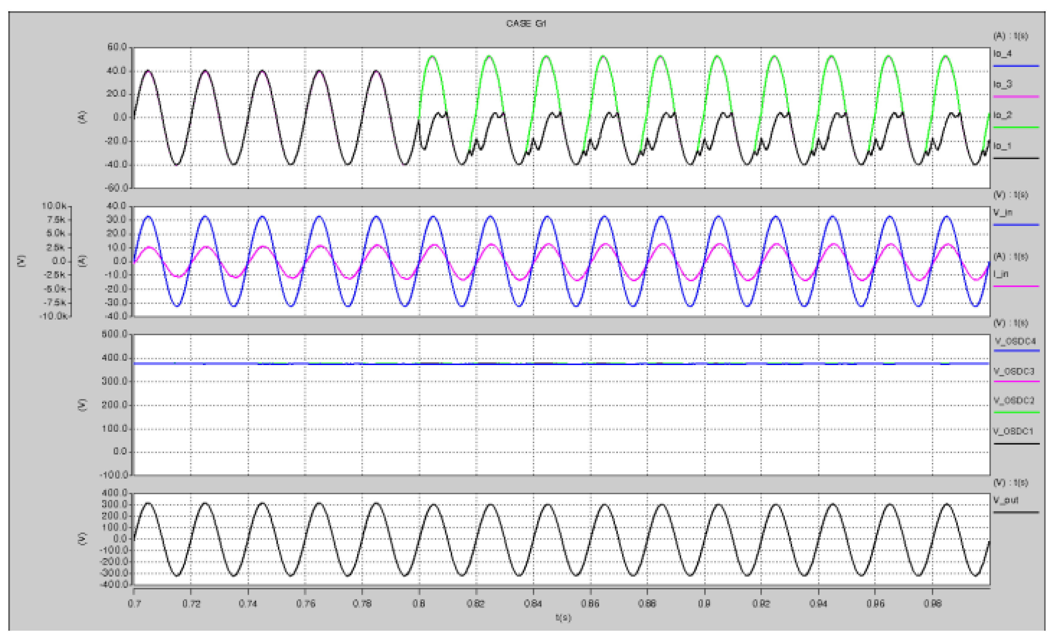
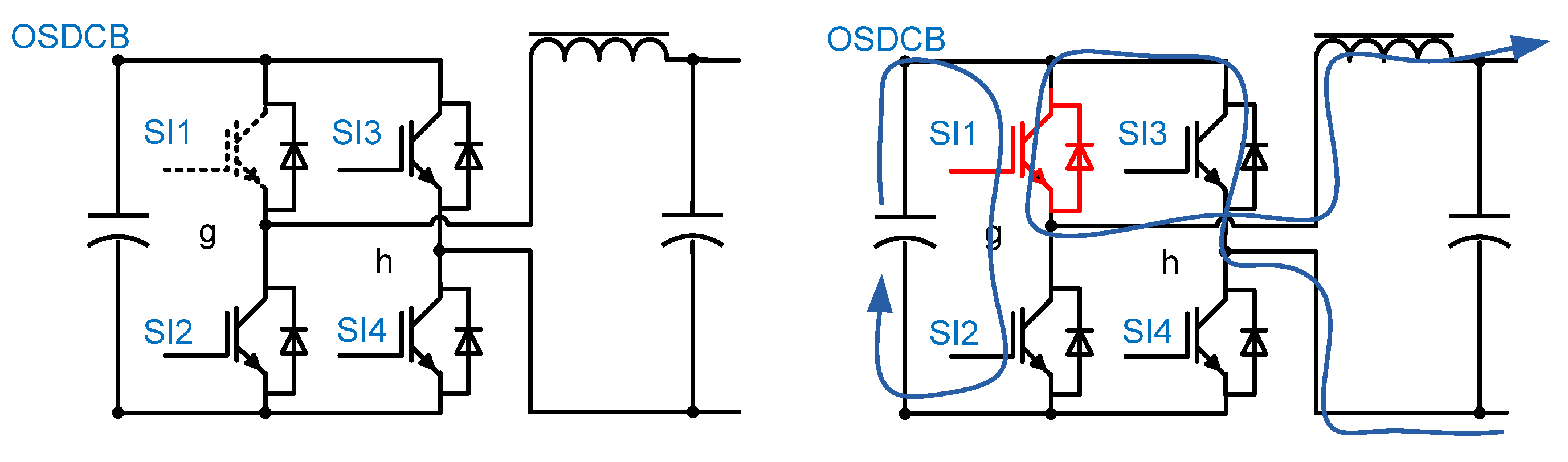
G1. Inverter IGBT Open-Circuit with Its Anti-Parallel Diode Normal
Figure 20 shows the G1 fault simulation results of the output currents of output stage modules (Io_4 to Io_1) which are in parallel with each other, the input voltage, input current, four OSDCB voltages, and the total output phase current (I_out). It can be observed that Io_1 can only flow in one direction since the fault happens, which makes Io_2, Io_3 and Io_4 increase in the same direction to cover the loss of Io_1, hence containing a dc component. The G2 fault case is similar to a G1 fault.
Figure 20.
Simulation results of faults G1 and G2.
Figure 20.
Simulation results of faults G1 and G2.
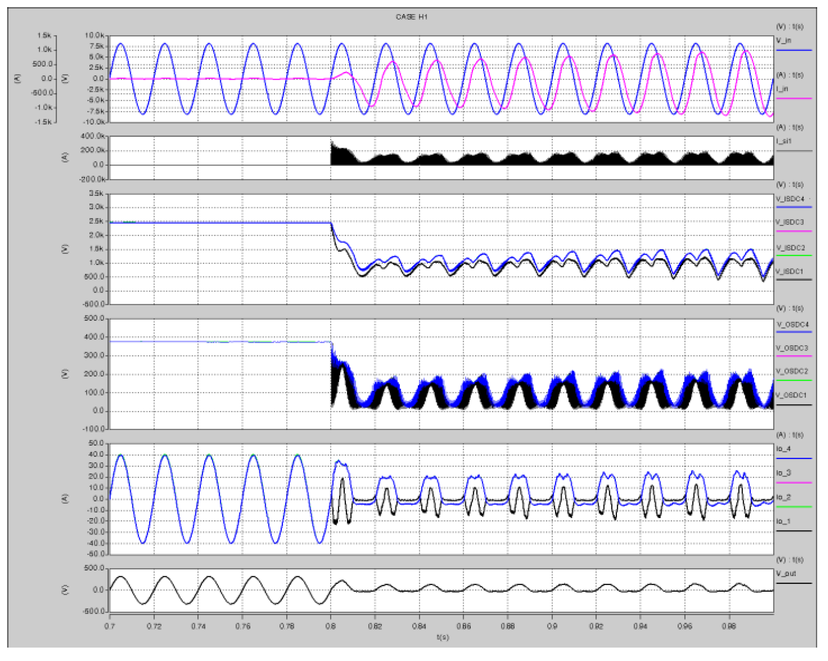
H1. Inverter IGBT Short-Circuit
Figure 21 shows the H1 fault simulation results of the input voltage, input current, the current through the shorted IGBT SI1 (I_si1), four ISDCB voltages, four OSDCB voltages, the output currents of output stage modules, and the total output phase current. It can be seen from the
Figure 21 that I_si1 increases to 200 kA at the moment of failure due to the shoot-through fault, hence resulting in a reduction on V_OSDC1. Meanwhile, the short-circuit path is shared by the output filter to the rest of OSDCB capacitors; hence all four OSDCB voltage will be reduced, as well as the four ISDCB voltages. Due to the abnormal OSDCB voltage, the output voltage is distorted as well.
Figure 21.
Simulation results of fault H1.
Figure 21.
Simulation results of fault H1.
6. Protection and Fault Diagnosis Strategy
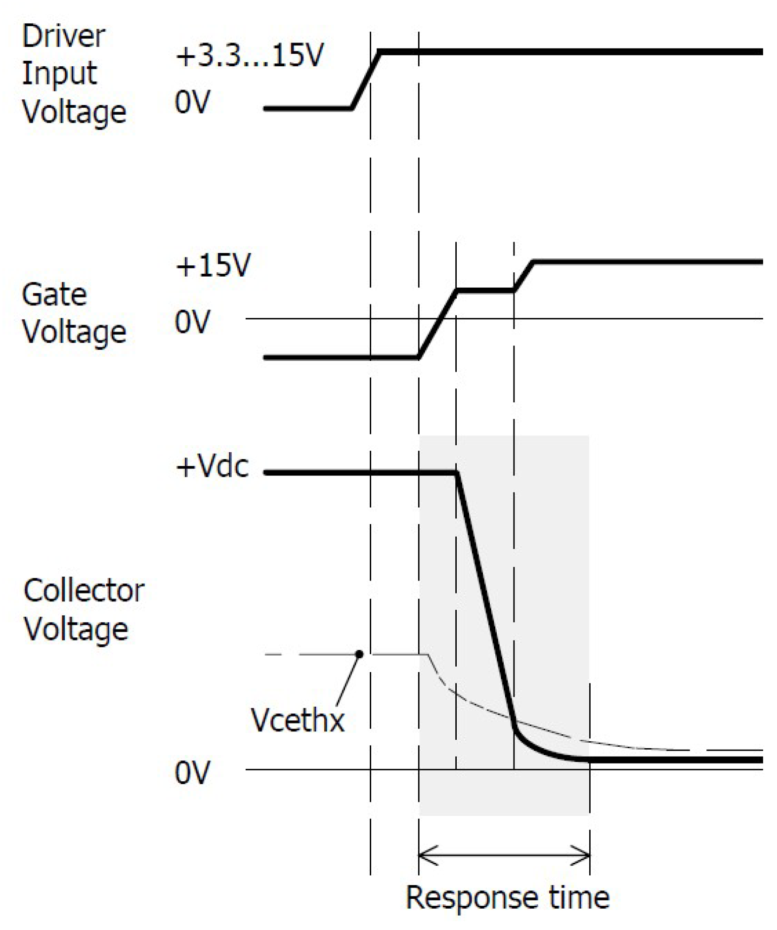
For short-circuit fault, the fault detection and protection should be very fast and based on the gate driver circuit of the power switch as the time between fault initiation and failure is very short. Take the IGBT driver 2SC0535T of CONCEPT (CT-Concept Technologie AG, Biel/Bienne, Switzerland) as an example, whose turn-on characteristics are shown in
Figure 22.
Each channel of the 2SC0535T driver is equipped with a Collector-Emitter-Voltage (Vce) monitoring circuit. The IGBT Collector-Emitter-Voltages are measured individually, and are checked after the response time at turn-on to detect a short circuit or over current. If the measured Vce at the end of the response time is higher than the dynamic threshold Vcethx, the driver detects a short circuit or over current. Then the driver turns the corresponding power switches off immediately, hence the consequent damages of the faults to the D-EPT are prevented. At the same time, the fault status is immediately transferred to the corresponding SOx output of the affected channel, which is usually connected to the I/O pins of DSP so that DSP would be aware of the faults. The power switch is kept in the off state (non-conducting) and the fault is shown at pin SOx as long as the blocking time is over or the fault is clear. Hence the short circuit fault protection based on hardware circuit is realized.
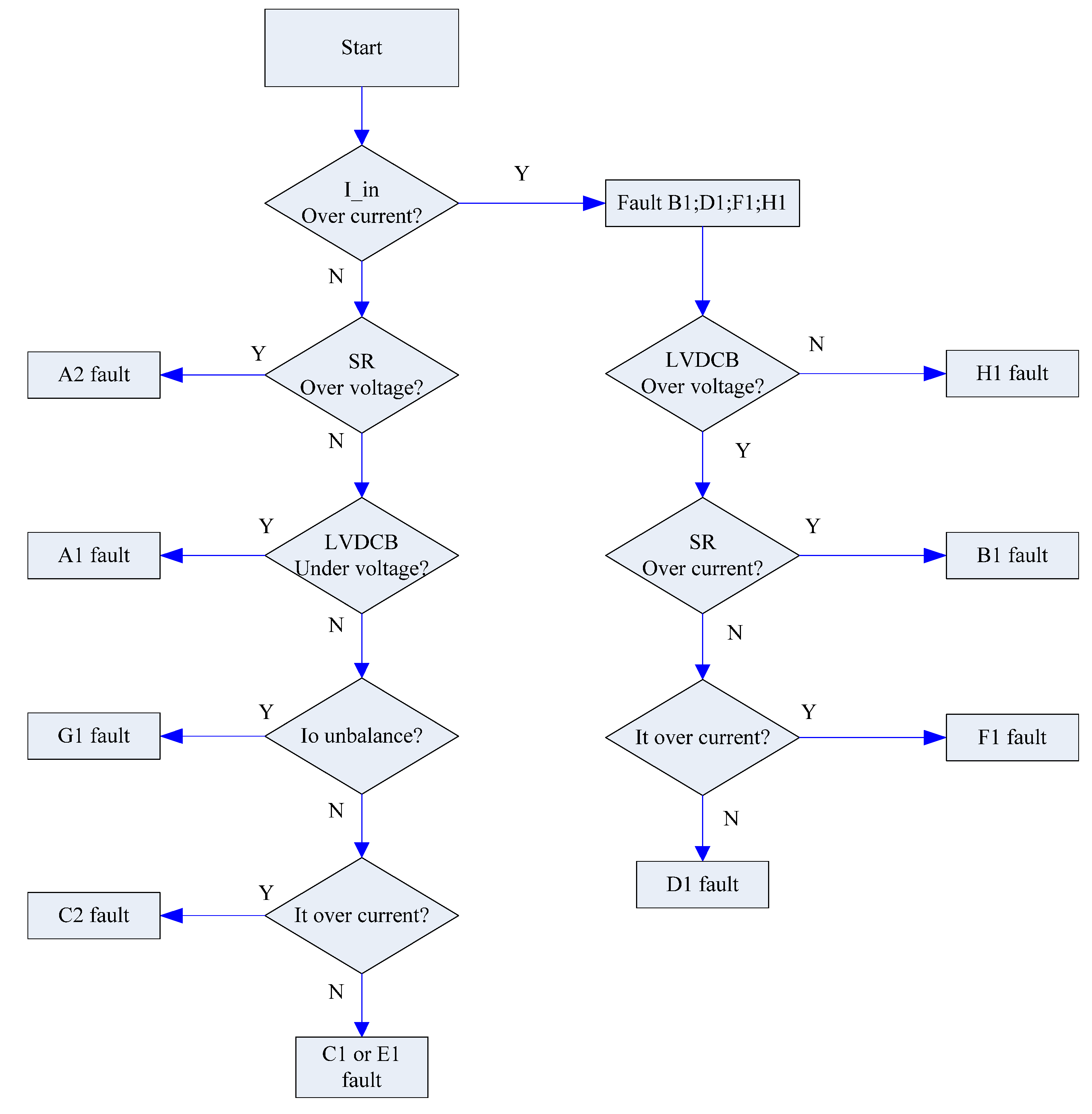
Based on the simulation results and
Table 1, the fault location algorithm of the power switches faults is shown in
Figure 23. As can be seen from this Figure, by monitoring the state of input current (I_in), the B1, D1, F1 and H1 faults which are all short-circuit faults, can be easily indicated, as short-circuit faults always reduce the resistance to the relevant part hence increasing the input current. By identifying the abnormal IGBT state which includes over voltage and over current, one can locate the failure part of the EPT easily.
Figure 22.
Turn-on characteristics of an IGBT.
Figure 22.
Turn-on characteristics of an IGBT.
Figure 23.
Flowchart for fault location algorithm.
Figure 23.
Flowchart for fault location algorithm.
As for open-circuit faults, a simple but effective way to identify the fault location from input stage (A1 and A2 faults), isolation stage (C1, C2, E1 and F1 faults), and output stage (G1 fault) is to monitor the abnormal states of relevant components. By applying current sensors and voltage sensors, these states of relevant components such as module output currents, transformer currents can be monitored. However, it is difficult to distinguish the C1 fault and E1 fault as the working power switches and working modes during those faults are exactly the same, hence with similar shapes of the waveforms.
Voltage and current sensors are needed to detect the abnormality of voltages and currents when faults occur. Based on
Table 1 which is concluded from the simulation results of
Section 5, the listed voltages and currents must be kept under monitoring, and treated in different ways.
First of all, the current sensor for input phase current (I_in) is needed, not only for input current over current, but also for the input factor abnormality. Hence a program should be applied not only to calculate the RMS value of input current, but also the input power factor.
Due to the EPT control scheme, only OSDCB voltages need to be monitored, hence reducing the cost and complexity which will increase greatly when it comes to the ISDCB voltages. The voltage sensors need to monitor the amplitudes of the DC voltages as well as their ripples. Moreover, some consequences of the faults will cause DC bus voltages to unbalance first, such as the case of the A1 or A2 faults, rather than under voltage and over voltage which are the worst case results. Hence the monitoring program needs to detect the amplitude and ripple voltage of each OSDCB voltage, and then check whether it is over voltage, under voltage, or unbalanced.
In the short-circuit fault, the fault detection and protection should be very fast and based on a hardware circuit as time between fault initiation and failure is very short. Therefore, the fault detection circuit should be embedded in each IGBT driver to detect the over voltage and over current faults for each IGBT.
The transformer currents are needed in order to detect the faults happening in the isolation stage of EPT, each one of which will cause transformer current abnormality including C1, C2, D1, E1, and F1 faults. The protection based on the RMS value is sufficient in many fields; however it is not enough for the detection of an isolation fault. According to the simulation results, the RMS value of transformer current is normal; however the amplitude of the current is already over the limit. Furthermore, the average current needs to be calculated to detect the transformer saturation problem. Hence the amplitude, RMS value and average value of transformer current are all needed.
In the output stage, the average value of each module output current is not zero after the G1 fault according to the simulation. Hence the output current of each module is also needed to calculate the amplitude, RMS value, and average value.
Finally, one needs to monitor the output voltage for its amplitude, RMS value and average value according to the simulation of the H1 fault.
The computational needs of DSP are RMS, amplitude and average values of voltage and current. The protection scheme would then compare them with the rated values to detect the faults, and the computational burden of all this s quite light for a 96 MHz TMS320F28335 DSP from Texas Instruments.


