Article

Fully Integrated on-Chip Switched DC–DC Converter for Battery-Powered Mixed-Signal SoCs

1
Samsung Electronics Co., Ltd., Gyeonggi-do 16677, Korea
2
Department of Electronic Engineering, Daegu University, Gyeongsan 38453, Korea
3
Department of Electrical and Computer Engineering, Northeastern University, 360 Huntington Ave., Boston, MA 02115, USA
*
Author to whom correspondence should be addressed.
Symmetry 2017, 9(1), 18; https://doi.org/10.3390/sym9010018
Submission received: 6 November 2016 / Revised: 27 December 2016 / Accepted: 10 January 2017 / Published: 22 January 2017
(This article belongs to the Special Issue Symmetry in Systems Design and Analysis)

Abstract

:
This paper presents a fully integrated on-chip switched-capacitor (SC) DC–DC converter that supports a programmable regulated power supply ranging from 2.6 to 3.2 V out of a 5 V input supply. The proposed 4-to-3 step-down topology utilizes two conventional 2-to-1 step-down topologies; each of them (2-to-1_up and 2-to-1_dw) has a different flying capacitance to maximize the load current driving capability while minimizing the bottom-plate capacitance loss. The control circuits use a low power supply provided by a small internal low-drop output (LDO) connected to the internal load voltage (VL_dw) from the 2-to-1_dw, and low swing level-shifted gate-driving signals are generated using the internal load voltage (VL_dw). Therefore, the proposed implementation reduces control circuit and switching power consumptions. The programmable power supply voltage is regulated by means of a pulse frequency modulation (PFM) technique with the compensated two-stage operational transconductance amplifier (OTA) and the current-starved voltage controlled oscillator (VCO) to maintain high efficiency over a wide range of load currents. The proposed on-chip SC DC–DC converter is designed and simulated using high-voltage 0.35 μm bipolar, complementary metal-oxide-semiconductor (CMOS) and DMOS (BCDMOS) technology. It achieves a peak efficiency of 74% when delivering an 8 mA load current at a 3.2 V supply voltage level, and it provides a maximum output power of 48 mW (IL = 15 mA at VL_up = 3.2 V) at 70.5% efficiency. The proposed on-chip SC voltage regulator shows better efficiency than the ideal linear regulator over a wide range of output power, from 2.6 mW to 48 mW. The 18-phase interleaving technique enables the worst-case output voltage ripple to be less than 5.77% of the load voltage.

1. Introduction

As the popularity of portable smart devices such as smart phones and tablet personal computers (PCs) continues to increase, the extension of battery-life time of smart devices has attracted much attention in recent years. To prolong the life of a battery that has limited energy capacity, the analog and digital modules in modern mixed-signal system on chips (SoCs) are designed to consume an extremely low amount of power (<10 mW). Since each module requires its own supply voltage, conventionally, a large number of linear regulators have been used as on-chip DC–DC converters to support the local power supplies from the global power supply. However, as voltage drops between the global power supply and the local power supplies increase, the collective power loss from the linear regulators becomes significant.
For this reason, developing more power-efficient alternatives that show low peak-to-peak output ripple voltage, with a minimal area cost of achieving higher efficiency in a wide range of the output load voltages, is required. Since on-chip capacitors have a significantly higher quality factor, higher energy density, and a lower cost than on-chip inductors in the standard complementary metal-oxide-semiconductor (CMOS) process, switched-capacitor (SC)-based on-chip DC–DC converters have been receiving increased attention from both academia and industry [1,2,3,4,5].
On-chip SC DC–DC converters can even save the total area significantly if metal-oxide-semiconductor (MOS) capacitors are used as flying (charge-transfer) capacitors and as load capacitors because MOS capacitors have higher density than metal-insulator-metal (MIM) or polysilicon-insulator-polysilicon (PIP) capacitors. The area benefits of using MOS capacitors will continue because the gate-oxide capacitance per unit area (Cox) of MOS capacitors has been increasing with continuous technology scaling. For example, the Cox for 1 μm technology (tox = 20 nm) is 1.75 fF/μm2, while the Cox for 50 nm technology (tox = 1.4 nm) is 25 fF/μm2 [6].
Moreover, since the on-resistance per unit area has been continuously decreasing with technology scaling, the size of MOS switches has decreased as well as they are designed to have the same on-resistances of the older technology. Therefore, the switching frequency of on-chip SC DC–DC converters can be increased to reduce the area of flying capacitors without compromising the efficiency. However, the bottom-plate parasitic capacitance of a MOS capacitor formed by the junction capacitance of drain/source terminals to the substrate (or bulk) is larger than that of MIM or PIP capacitors; it can be as large as 10% of the actual capacitance. Therefore, if MOS capacitors are used as flying capacitors, the loss due to the bottom-plate capacitors is significant. For example, with a 10% bottom-plate capacitance ratio (α), the overall efficiency of the conventional 2-to-1 step-down topology can drop more than 20% when compared to the case with a 0% bottom-plate capacitance ratio (α) when it delivers 85% of the no-load voltage.
In this paper, a new power-efficient 4-to-3 step-down SC topology is proposed to provide a regulated power supply ranging from 2.6 V to 3.2 V out of a 5 V input supply with a novel programmable feature whose efficiency is less sensitive to increasing the bottom-plate capacitance ratio (α) than the conventional SC topologies. The proposed design is implemented with the on-chip MOS capacitors only without any external components. Section 2 presents the operating principle of the proposed on-chip SC DC–DC converter and the optimum design methodology in terms of the maximum charge transfer to the load with the minimum loss. The system architecture and simulation results are presented in Section 3 and Section 4, respectively, followed by the conclusion in Section 5.

2. Core Design

2.1. Operating Principle

In general, the SC DC–DC converter consists of capacitors and switches, which are driven by two non-overlapping clock signals. The clock signals are set as close as 50% duty cycle with a minimal dead-time (n-channel metal-oxide semiconductor (NMOS) and p-channel metal-oxide semiconductor (PMOS) switches are never closed at the same time to prevent the shoot-through current loss) for the maximum efficiency and the maximum charge transfer to the load. 
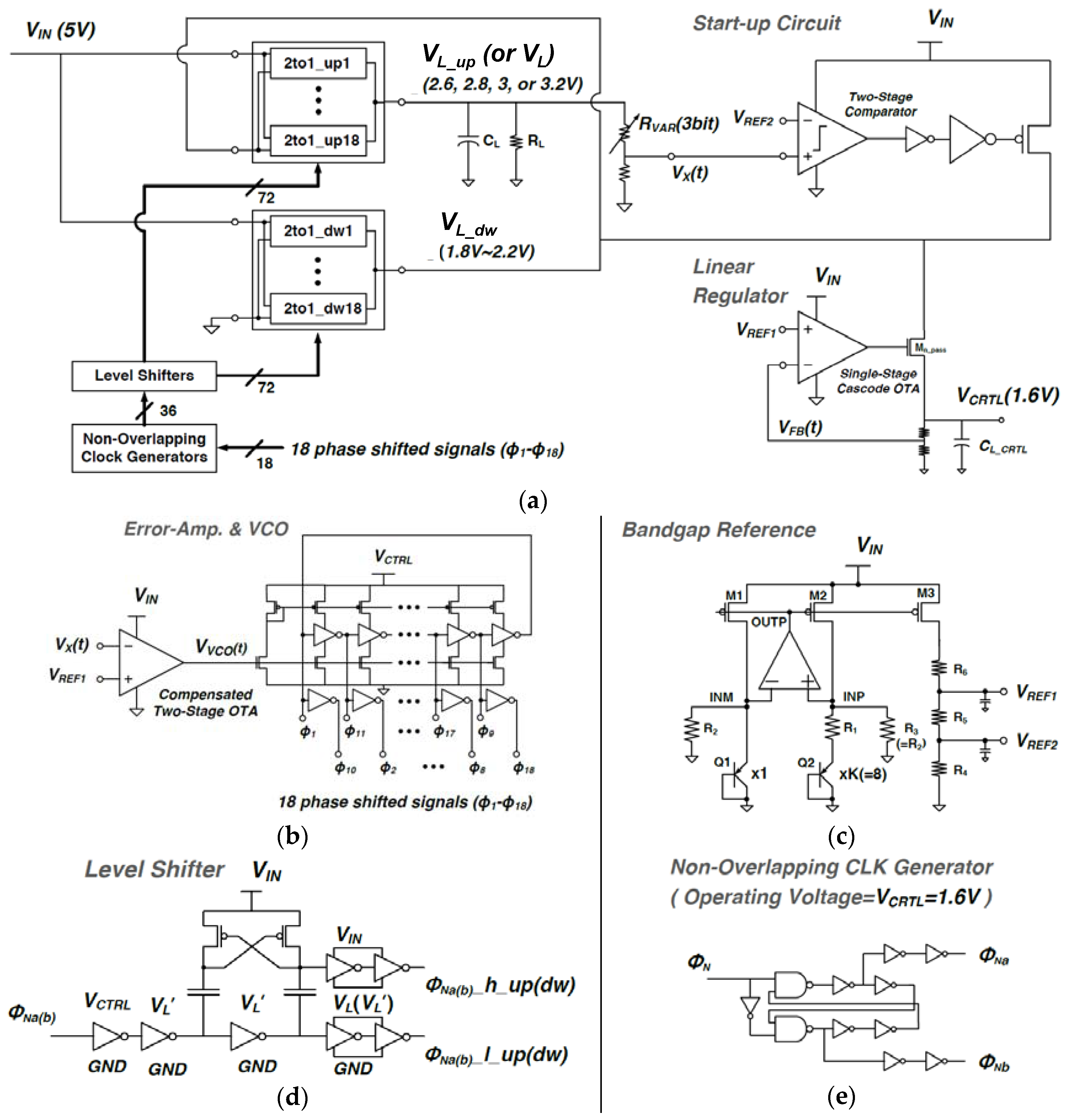
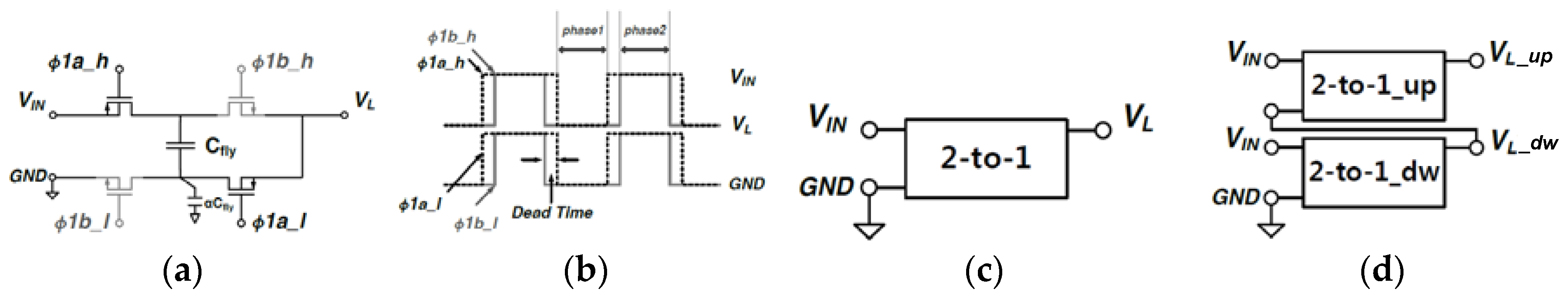
Figure 1a, b shows the conventional 2-to-1 topology and its low-swing gate-driving signals, respectively. The signals are generated from the level-shifters followed by the non-overlapping clock generators, which will be shown later in Figure 5 in Section 3 to minimize the switching loss. To present the loss due to bottom-plate parasitic capacitors, a bottom-plate parasitic capacitor is modeled as αCfly, where Cfly is the actual capacitance of a flying capacitor and is the process and layout-dependent parameter. For convenience, Figure 1a can be symbolized as the one shown in Figure 1c, which has two input terminals and one output terminal. Assuming that (1) all MOS switches have the same on-resistance of Ron; (2) the time durations of phase1 and phase2 are the same with the minimal dead time; and (3) the time constant (RL + 2Ron)Cfly is much larger than 1/(2fsw), the average load voltage (VL) in Figure 1a,c, is defined as the average voltage between two input voltages (=(VIN + 0 V)/2 = VIN/2) minus ΔVL, since the average voltage across the flying capacitor (Cfly) is constant at VIN/2 in steady-state. ΔVL results from the conduction loss and can be given by:
Δ V L = ( 1 R L R L + 2 R o n ) V N L .
As shown in Equation (1), if the MOS switches have zero on-resistance, ΔVL becomes zero; therefore, no conduction loss exists, and the average load voltage (VL) will be the same as the no-load voltage (VNL = VIN/2).
In a similar way, the proposed 4-to-3 topology is created in a combination of two 2-to-1 topologies as shown in Figure 1d; one input terminal of the 2-to-1_up block is fed directly from the input voltage source (VIN), and the other input terminal is fed out of the output (VL_dw) of the 2-to-1_dw block. Therefore, the generated load voltage VL_up (=(VIN + VL_dw)/2 − ΔVL_up) is the average value of VIN and VL_dw (=1/2VIN − ΔVL_dw) minus ΔVL_up. ΔVL_up and ΔVL_dw represent the voltage difference between the delivered load voltages when there is load and there is no load. Again, ΔVL_up and ΔVL_dw arise from the conduction loss, and they limit the maximum attainable efficiency to ηlin = VL_dw/(1/2VIN) for 2-to-1_dw and ηlin = VL_up/{(VIN + VL_dw)/2} for 2-to-1_up.
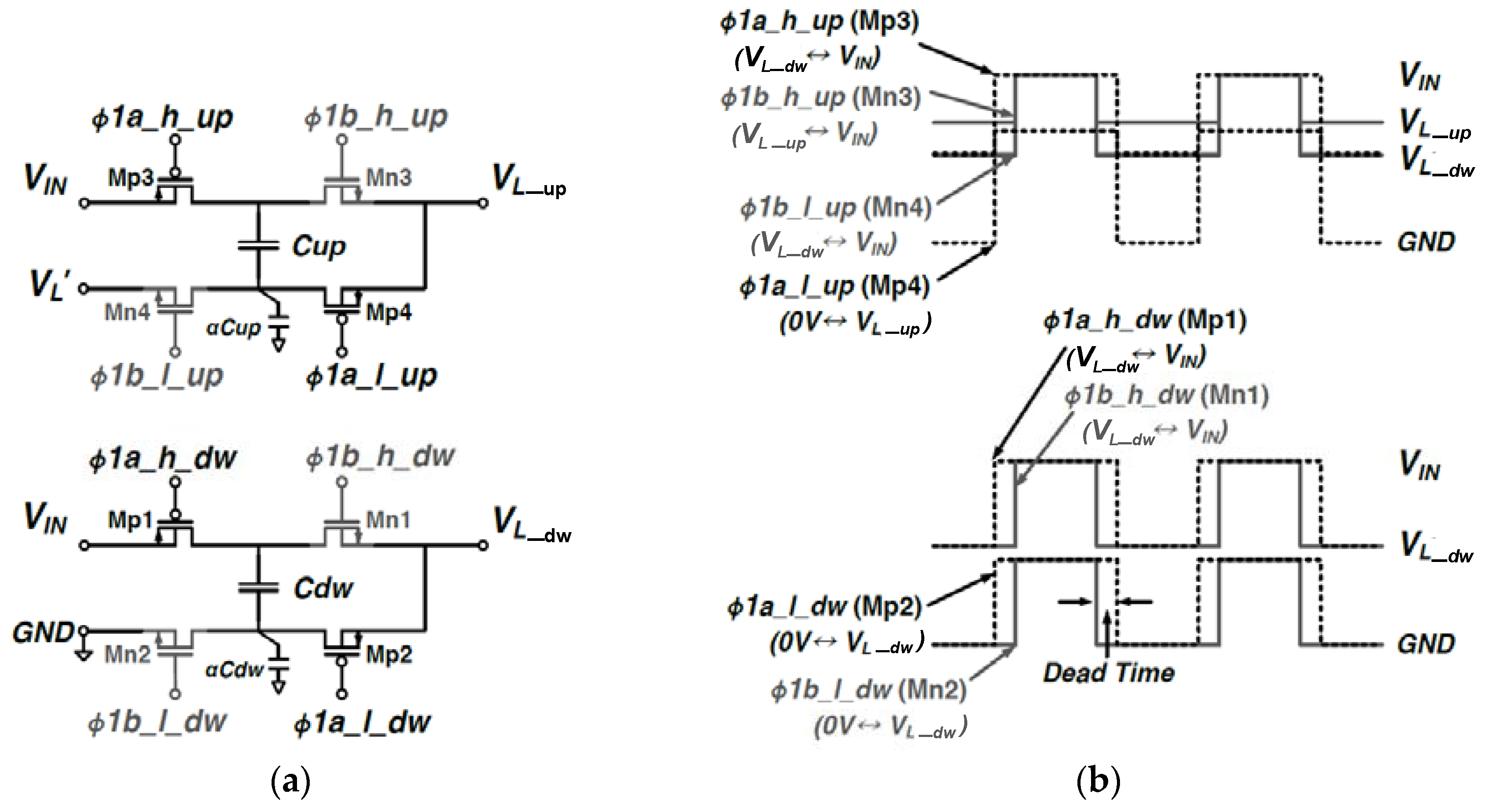
Figure 2a shows the transistor level implementations of the 2-to-1_dw(up) blocks, and Figure 2a shows the gate-driving signals. Since the gate-oxide breakdown voltage of 5 V CMOS transistors in 0.35 μm BCDMOS technology is 5.5 V, all switches can withstand any voltage levels between ground (0 V) and input (5 V). All the gate driving signals in Figure 2b are generated from the level shifters and the non-overlapping clock generators to minimize the switching loss and shoot-through current loss, which will be shown in Figure 5 in Section 3. The NMOS transistors (Mn1, Mn3, and Mn4) in Figure 2a are implemented by means of a triple-well device to isolate the body voltage from the substrate (or bulk).

2.2. Charge Transfer and Loss Mechanisms

The 2-way interleaved structure of the proposed SC DC–DC converter shown in Figure 3a is used for simplicity of the analysis. For the gate driving signals, ϕ1a (ϕ1b) and ϕ2a (ϕ2b) are 180° out of phase signals, while ϕ1a (ϕ2b) and ϕ1b (ϕ2b) represent non-overlapping clock signals, which are shown in Figure 2b. Figure 3b represents the equivalent circuit during every half period (phase1 and phase2) of the switching frequency. Assuming that the SC DC–DC converter delivers charge to the loads at average voltages of VL_up (or VL) and VL_dw, the charge extracted from the input voltage source (QEXT(VIN)) during every half period of the switching frequency (when the MOS transistors which have the gate-driving signals of ϕ1a (ϕ1b) and ϕ2b (ϕ2a) are on) can be derived as:
Q E X T ( V I N ) = C u p ( Δ V L _ u p ) + C d w ( Δ V L _ d w ) .
Since the total charge delivered to the load (VL_up) is the sum of the charge transferred from both top flying capacitors (Cup/2) as shown in Figure 3b, the total charge transferred to the load is given by:
Q L = 2 C u p ( Δ V L _ u p ) .
Considering only the charge transfer, the efficiency can be defined as the ratio of the total charge delivered to the load shown in Equation (3) to the charge extracted from the input voltage source shown in Equation (2). The relationship between ΔVL_up and ΔVL_dw is determined by the ratio between Cup and Cdw, which will be derived in Equation (6). By solving Equations (2) and (6) together, the efficiency of the proposed 4-to-3 step-down SC DC–DC converter is given by VL_up/(3/4VIN (=VNL)). It shows the upper limit of the efficiency of any kind of SC DC–DC converters; in other words, the maximum attainable efficiency decreases as the voltage drop between the no-load voltage (VNL) and the average load voltage (VL_up) increases.
In order to determine the minimum required capacitances for each flying capacitor that satisfy the design requirements (IL(MAX) = 10 mA and VL_up = 3.2 V @ƒsw(MAX) = 13 MHz), the load current driving capability of the proposed SC DC–DC converter has to be derived in terms of Cfly, ΔVL, and ƒsw(MAX). From Equations (2) and (3), and Figure 3b, the load current driving capability at a fixed switching frequency (ƒsw) and ΔVL (=ΔVL_up + 1/2ΔVL_dw since ΔVL = VNLVL_up, where VNL = 3/4VIN and VL_up = (VIN + VL_dw)/2 − ΔVL_up) is given by:
I L = 2 I 1 = 4 C u p Δ V L _ u p   f s w
I 1 = 2 I 2 I c t r l 2 I 2 = 4 C d w Δ V L _ d w   f s w .
From Equations (4) and (5), the relationship between ΔVL_up and ΔVL_dw is determined by the ratio between Cup and Cdw, which is given by:
Δ V L _ u p Δ V L _ d w = 2 C d w C u p .
There is an optimal ratio between Cup and Cdw, which yields the maximum load current (IL) at a constant ΔVL_dw, ƒsw, and Cfly. Since VL_up is the summation of ΔVL_up and 1/2ΔVL_dw, ΔVL_up can be express in terms of ΔVL_dw, Cup (=CflyCdw), and Cdw using Equation (6) as:
Δ V L _ u p = 4 C d w 3 C d w + C f l y Δ V L .
From Equations (4) and (7), the load current (IL) is given by:
I L = 16 Δ V L f s w C f l y C d w C d w 2 3 C d w + C f l y .
By taking the partial derivative of Equation (8) with respect to Cdw and putting it to zero, the maximum load current (IL(MAX)) is obtained when Cfly is three times that of Cdw. Therefore, the optimal ratio between Cup and Cdw, which yields the maximum load current (IL) at a constant ΔVL, ƒsw, and Cfly (=Cup + Cdw), is given by Cup = 2Cdw. Therefore, Equation (8) can be rewritten as:
I L ( M A X ) = 16 3 C d w Δ V L f s w = 16 9 C f l y Δ V L f s w
where C f l y = C u p + C d w , C u p = 2 C d w .
From Equation (6), if Cup is twice the value of Cdw, ΔVL_up is equal to ΔVL_dw. Since our target load voltage is 3.2 V, ΔVL is determined to be 0.55 V (ΔVL = ΔVNLVL_up). Therefore, both ΔVL_up and ΔVL_dw are determined to be about 0.367 V, since ΔVL is equal to the summation of ΔVL_up and 1/2 ΔVL_dw. For the given specifications, (1) ΔVL_up (=ΔVL_dw) is 0.367 V; (2) the maximum load current (IL(MAX)) is 10 mA; and (3) the maximum switching frequency (ƒsw) of the voltage controlled oscillator (VCO) is about 13 MHz, and the minimum required Cup can be estimated as about 455 pF. Considering process–voltage–temperature (PVT) variations, the Cup of 600 pF and Cdw of 300 pF are chosen. The MOS switches are sized with small margins to guarantee that the converter is able to deliver a 10 mA load current to the 3.2 V load.
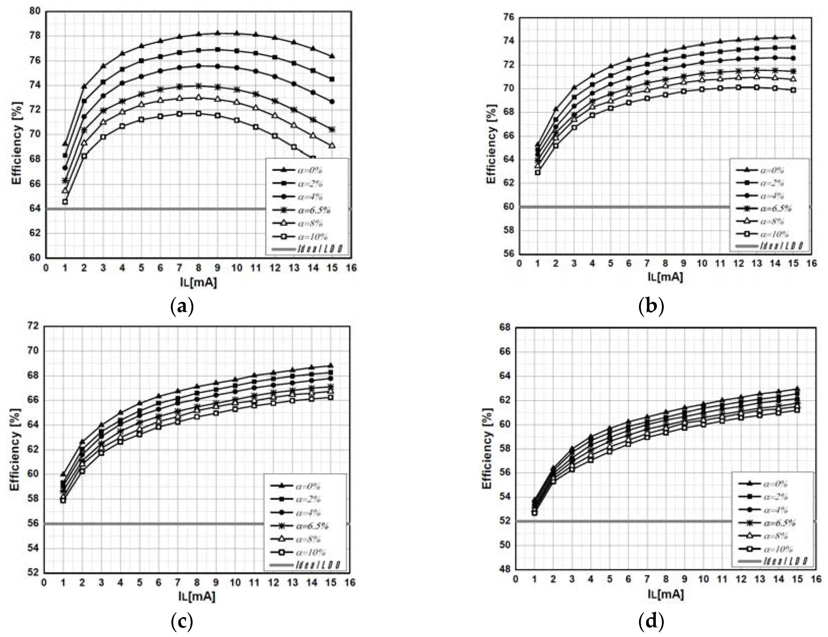
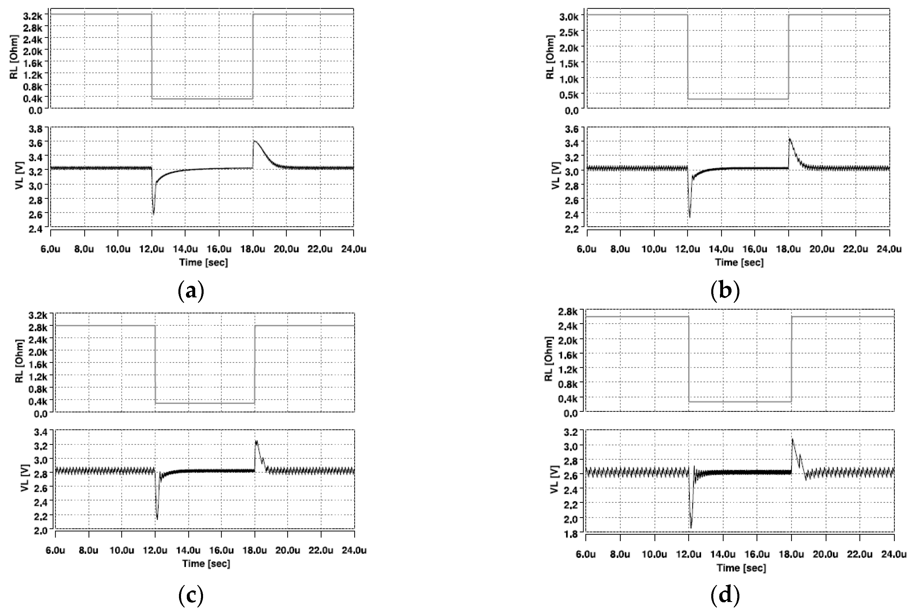
As can be observed from Equation (9), with the fixed values of ΔVL and Cup (Cdw), the load current (IL) can be controlled by changing switching frequency (ƒsw). Therefore, with a change in load current, the output load voltage can be regulated by means of pulse frequency modulation (PFM). In this design, the PFM control scheme is used with the compensated two-stage operational transconductance amplifier (OTA) and the current-starved voltage controlled oscillator (VCO) as shown in Figure 5, which are designed to be operating in the range of 0.44 MHz to 15 MHz. Therefore, switching and bottom-plate capacitance loss are the maximum at the heaviest load condition (IL = 10 mA at VL_up = 3.2 V) and scale down linearly with the decreasing load by means of PFM technique.
Besides the conduction loss, the loss due to the bottom-plate parasitic capacitors is significant, especially when on-chip capacitors are used as flying capacitors. Since MOS capacitors (2.7 fF/μm2) have higher capacitance density than MIM capacitors (1 fF/μm2) in BCDMOS 0.35 μm technology, only MOS capacitors are used as the flying and load capacitors. In this case, the bottom-plate capacitance ratio (α) is assumed to be 6.5% of an actual capacitance. As shown in Figure 3b, during every half period of the switching frequency, each top bottom-plate capacitor αCup/2 (αCdw/2) in 2-to-1_up(dw) is charged to VL_up (VL_dw), while each bottom bottom-plate capacitor αCup/2 (αCdw/2) is discharged to VL_dw (0 V). While the charged electrons in the bottom-plate capacitors of the 2-to-1_dw block are discharged to ground, the charged electrons in the bottom-plate capacitors of 2-to-1_up block are discharged to the load VL_dw. As a result, the energy lost per cycle due to those bottom-plate capacitors can be given by:
E B P = α C u p ( V L _ u p V L _ d w ) 2 + α C d w V L _ d w 2 .
Assuming the bottom-plate capacitance ratio (α) is 0%, Equation (9) can be used to verify the previous analysis.To determine the optimum ratio between Cup and Cdw with non-zero, Cup is swept from 450 pF to 700 pF at a different bottom-plate capacitance ratio (α). Cup is altered from 0% to 10% while the total flying capacitance Cfly is maintained at 900 pF. As shown in 
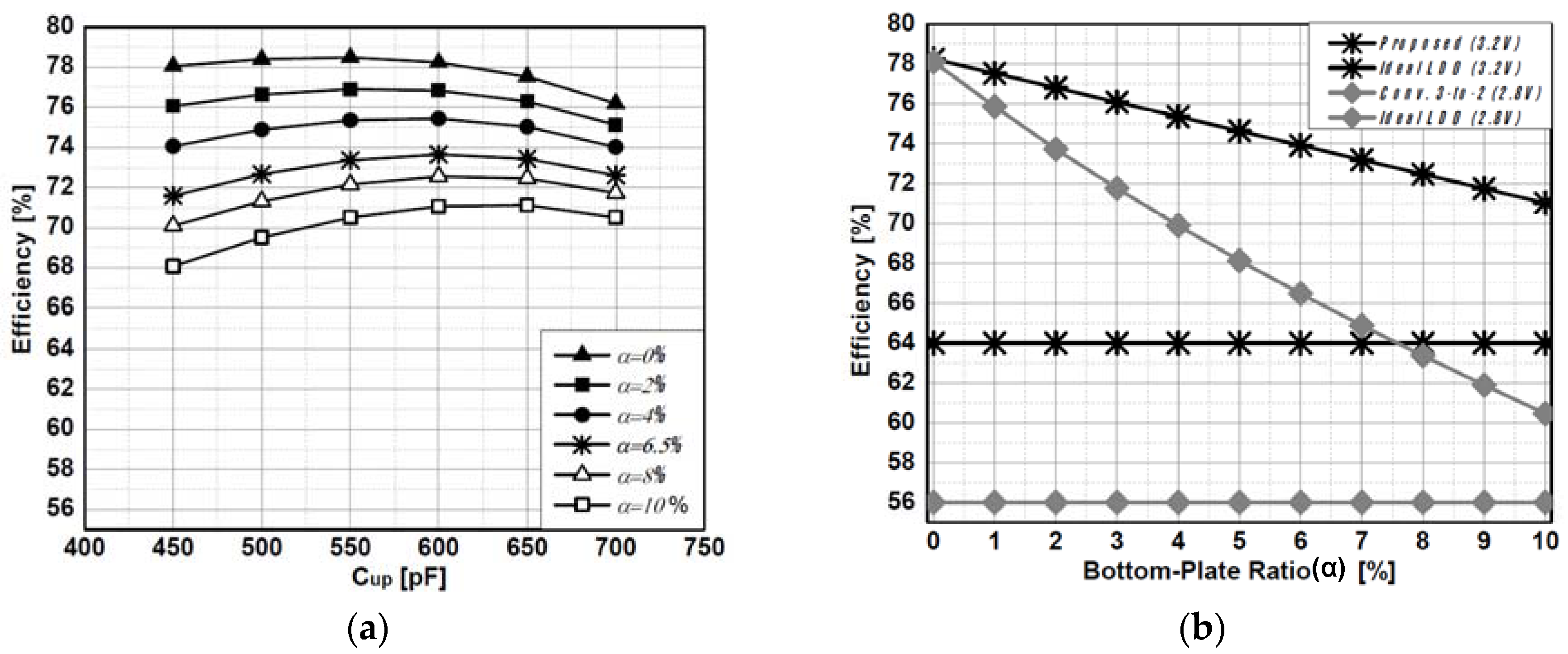
Figure 4a, the maximum efficiency of 78.5% is obtained when Cup is 550 pF and α is 0%. According to Equation (9), the maximum load is supposed to be obtained when Cup is twice the value of Cdw; that is, Cup = 600 pF. The discrepancy can be explained from the neglected control current (Ictrl) in Equation (5). However, as α increases from 0% to 10%, the maximum efficiency points in Figure 4a moves to the right hand side of the x-axis while the overall efficiency decreases linearly, which can be explained with Equation (10). However, as shown in Figure 3b, since the voltage swing (VL_upVL_dw) at the top bottom-plate capacitors (Cup/2) is always smaller than the voltage swing (VL_dw) at the bottom bottom-plate capacitors (Cdw/2) for the range of Cup between 450 pF and 700 pF, the energy loss due to the bottom-plate capacitor is reduced as Cup increases. As the maximum efficiency of 73.5% is obtained when Cup is 600 pF and is 6.5% from Figure 4a, Cup and Cdw are selected to be 600 pF and 300 pF, respectively, for the implementation.
Figure 4b shows the efficiency drop of the proposed 4-to-3 topology and the conventional 3-to-2 topology [1] with respect to increasing α. In both cases, load voltages are regulated at ~85% of the no-load voltages (3.75 V for 4-to-3 topology and 3.33 V for 3-to-2 topology), while delivering a 10 mA load current using the same amount of flying and load capacitors, the same control scheme, and the same bias circuits for the implementation of both SC DC–DC converters. As shown in Figure 4b, with an increasing bottom-plate capacitance ratio (α) from 0% to 10% of the flying capacitors, the efficiency drop of the proposed 4-to-3 topology is less than 8%, which is 2.25 times less than that of the conventional 3-to-2 topology.

3. Architecture

Figure 5 shows the architecture of the proposed SC DC–DC converter. The complete system consists of 18-phase 2-to-1_up (dw) blocks, 72 level shifters, 18 non-overlapping clock generators, an error-amplifier, a current-starved voltage controlled oscillator (VCO), an NMOS pass transistor-based low-drop output (LDO) linear regulator, a start-up circuit, and a bandgap voltage reference. Each of the 2-to-1_up blocks employs a 33.33 pF MOS capacitor (the total capacitance of 600 pF for 18 phases) for its flying capacitor, while each 2-to-1_dw block employs a 16.66 pF MOS capacitor (the total flying capacitance of 300 pF for 18 phases). The output buffer capacitor of 400 pF is used to reduce the output ripple and to support the moderate level of transient response under the load current variations.
As shown in Figure 5, the start-up circuit and load regulation circuits (error-amplifier and linear regulator) of the proposed architecture are based on two reference voltages (VREF1 and VREF2) from a modified single bandgap voltage reference, which is based on Reference [7]. Once the internal load voltage (VL_dw) is charged up to about 1.8 V by start-up circuit, the power supply voltage of the control circuits (VCTRL) is regulated at 1.6 V by NMOS pass transistor-based low-drop out (LDO) voltage regulator connected to the internal load voltage (VL_dw), which is the output voltage of the 2-to-1_dw. Therefore, the reduction of control loss is achieved by decreasing the dynamic power consumption in the current-starved VCO and 18 non-overlapping clock generators. In addition, the internal load voltage (VL_dw) is used to generate low swing level-shifted gate-driving signals to reduce switching loss.
The output power supply voltage can be set to 2.6 V, 2.8 V, 3 V, or 3.2 V using a digitally controlled 3-bit resistor divider network. Each level of the output power supply voltages is regulated by means of a pulse frequency modulation (PFM) technique with the compensated two-stage operational transconductance amplifier (OTA) and the current-starved VCO to maintain high efficiency over a wide range of load currents. As the scaled load voltage (Vx(t)), which is set by a 3-bit resistor divider network, becomes less than VREF1, the output voltage (VVCO(t)) of the error-amplifier increases, and vice versa; thus, the oscillation frequency of the current-starved ring oscillator increases or decreases until Vx(t) is equal to VREF1. The 18-phase interleaved structure is used to reduce the output ripple voltage. The equally phase-shifted 18-phase interleaved signals are generated from the current-starved ring oscillator and inverters, and they become the low swing gate-driving signals using the non-overlapping clock generators and the level shifters to reduce the gate-drive switching loss.

4. Simulation Results

The proposed on-chip SC DC–DC converter is designed and simulated using high-voltage 0.35 μm BCDMOS technology. Figure 6 shows the efficiency comparison between the proposed on-chip SC DC–DC converter and the ideal linear regulator when they deliver a different load current (IL) between 1 mA and 15 mA at four different output load voltage levels (VL or VL_up, henceforth referred to as VL). The efficiency is also shown for a different bottom-plate capacitance ratio (α) between 0% and 10%. In order to effectively visualize the degrees of the efficiency drop, which increase when the proposed converter is set to support one of four different output load voltage levels (3.2 V, 3 V, 2.8 V, and 2.6 V), the scale of the y-axis is adjusted to show the maximum efficiency change of 20%.
The proposed on-chip SC DC–DC converter shows 74% peak efficiency when it delivers an 8 mA load current at a 3.2 V load voltage level, which is shown in Figure 6a. Since the output power supply voltage is regulated by means of a PFM technique with the change of load current, the switching frequency (ƒsw) scales with the load power. As the load power decreases, the losses due to the switching loss and the bottom-plate capacitance decrease as well. Therefore, the proposed converter provides higher efficiency over a wide output power range between 2.6 mW and 48 mW than the ideal linear regulator. However, since the static control power does not scale with the switching frequency, the portion of the control power loss becomes dominant as the load power decreases, causing the overall efficiency to decrease. As the regulated load voltage is set to 2.8 V from 3.2 V, the efficiency drop becomes less sensitive to the increase since the voltage swings at the bottom-plate capacitors decrease, as presented in Equation (10), and the conduction loss becomes more dominant than the bottom-plate capacitance loss.
Figure 7 shows the transient responses at four different load voltage levels when the load current (IL) changes from 1 mA to 10 mA, and vice versa. The worst-case transient response occurs with the load current transition from 10 mA to 1 mA when the load voltage is regulated at 3.2 V; the recovery time is about 2 μs, while the average response time of the load current variation between 10 mA (1 mA) and 1 mA (10 mA) is less than 1.5 μs. The worst-case peak-to-peak output ripple voltage occurs when the proposed SC DC–DC converter delivers a 1 mA load current to a 2.6 V load voltage as shown in Figure 7d; it is about 150 mV and 5.77% of the load voltage (VL = 2.6 V) when the output buffer capacitor of 400 pF is added to the load.
Figure 8 shows the output load voltage (VL) and the efficiency variations with process–voltage–temperature (PVT) variations when the proposed SC DC–DC converter delivers a 10 mA load current at four different output load voltage levels. For the process variation, device mismatches such as threshold voltage (Vto), current factor (β = μoCox), and base-to-emitter voltage (Vbe(eb)) variations are considered. In addition to the components’ statistical variation provided by the fabrication vendor, an intentional 20% capacitance variation (at 3-sigma) in flying capacitors are considered. A 3% supply voltage variation at 3-σ at different temperatures is considered as well. In order to extract the average and 1-sigma variations of the output load voltage and the efficiency, 100 transient Monte Carlo (MC) simulations are performed at different temperatures.
Since the proposed SC DC–DC converter regulates its load voltage (VL) until the down-scaled load voltage (VX(t)) in Figure 5 in Section 3 is equal to the reference voltage (VREF1) from the bandgap voltage reference, VL can be regarded as the up-scaled reference voltage. Therefore, each average load voltage (VL) in Figure 8 has a parabolic shape with respect to temperature since the reference voltage from bandgap voltage reference has a parabolic shape with respect to temperature as well. The degree of load voltage and efficiency variations increases rapidly when the proposed converter supplies a 3.2 V load voltage and a 10 mA load current. As the load voltage level (VL) increases, ΔVL decreases requiring a higher switching frequency (ƒsw) to deliver the same load current (IL = 10 mA), as explained in Equation (9). In addition, since the maximum frequency generated from the VCO decreases with increasing temperature, when the same voltage of VVCO(t) is applied to the input of the VCO as shown in Figure 5 in Section 3, the shape of the average load voltage (@VL = 3.2 V) in Figure 8a shows a slightly different parabolic shape. That is, the peak load voltage occurs at a temperature of 25 °C and the average load voltage decreases faster from that point than the other load voltages in Figure 8b,c. This means that the switching frequency (fsw) generated from the VCO is reached at its maximum value (fsw(MAX)) when the temperature is around 25 °C; therefore, the load voltage drops faster than the other load voltages. The average efficiency drops faster with increasing temperature due to increased conduction loss. The worst-case percent variations occur when the converter delivers a 2.6 V load voltage at 100 °C temperature; the percent variation of the average load voltage is about 0.68%, while the percent variation of the average efficiency is about 2.47% at 1-σ The simulation results confirm that the load regulation and the efficiency of the proposed SC DC–DC converter is robust with PVT variations.
A comparison with recently published SC DC–DC converters is listed in Table 1. Since the proposed SC DC–DC converter design only uses high capacitance density on-chip MOS capacitors as the flying capacitors (900 pF) and the load capacitor (400 pF), it maximizes the power density (48 mW), while it saves the area required for on-chip pads and integrated circuit (IC) pins to the external capacitors. At the same time, the fully on-chip solution minimizes parasitic components such as equivalent resistance (ESR), equivalent inductance (ESL), and equivalent series capacitance (ESC), which may cause large switching noises, resulting from the bonding, packaging, and PCB wiring. In addition, the proposed design can provide a high load current up to 15 mA with only 900 pF of flying capacitors since it employs a wide range of PFM techniques for its load regulation. Furthermore, since the efficiency of the proposed topology is less sensitive to the increasing bottom-plate capacitance ratio (α), the best peak efficiency (74%) is obtained even though only MOS capacitors (α = 6.5%) are used as its flying capacitors. The 18-phase interleaving techniques provide the worst-case output ripple voltage, which is about 5.77% of the load voltage (VL = 2.6 V) when the proposed SC DC–DC converter delivers a 1 mA load current. A 5.77% worst-case ripple voltage is obtained with the smallest on-chip load capacitor (400 pF) compared to other SC DC–DC converter designs, and it can be further reduced by employing a larger load capacitor at an increasing cost/area. The switching frequency (fsw) range is from 0.44 to 15 MHz, and the average load voltage range is from 2.6 to 3.2 V.

5. Conclusions

This paper presents a novel fully integrated on-chip SC DC–DC converter that supports a programmable regulated power supply ranging from 2.6 to 3.2 V out of a 5 V input supply. The proposed design employs only MOS capacitors for the flying capacitors (900 pF) and the load capacitor (400 pF) to maximize the power density. In addition, the proposed design can provide a high load current up to 15 mA with only 900 pF of flying capacitors since it employs a wide range of PFM techniques for its load regulation. The efficiency of the proposed converter is 2.8 times less sensitive to the increasing bottom-plate capacitance ratio (α) than the conventional 3-to-2 topology due to its unique structure. The programmable output voltage is regulated by means of a PFM technique with the compensated two-stage OTA and the current-starved VCO. The switching frequency (fsw) range is from 0.44 to 15 MHz, and the average load voltage range is from 2.6 to 3.2 V. The proposed converter achieves a peak efficiency of 74% when it delivers an 8 mA load current at a 3.2 V load voltage. The proposed converter shows better efficiency than the ideal linear regulator over a wide range of output power, from 2.6 to 48 mW. The 18-phase interleaving technique enables the worst-case output voltage ripple to be less than 5.77% of the load voltage.

Author Contributions

Heungjun Jeon carried out the genetic studies, researched articles, and simulated the proposed design. Yong-Bin Kim and Kyung Ki Kim analyzed the simulation results and advised overall. All authors read and approved the final manuscript.

Conflicts of Interest

The authors declare no conflict of interest.

References

  1. Ramadass, Y.; Fayed, A.; Chandrakasan, A. A fully-integrated switched-capacitor step-down DC-DC converter with digital capacitance modulation in 45 nm CMOS. IEEE J. Solid-State Circuits 2010, 45, 2557–2565. [Google Scholar] [CrossRef]
  2. Le, H.-P.; Sanders, S.; Alon, E. Design techniques for fully integrated switched-capacitor DC-DC converters. IEEE J. Solid-State Circuits 2011, 46, 2120–2131. [Google Scholar] [CrossRef]
  3. van Breussegem, T.; Steyaert, M. Monolithic capacitive DC-DC converter with single boundary-multiphase control and voltage domain stacking in 90 nm CMOS. IEEE J. Solid-State Circuits 2011, 46, 1715–1727. [Google Scholar] [CrossRef]
  4. Jain, R.; Sanders, S. A 200 mA switched capacitor voltage regulator on 32 nm CMOS and regulation schemes to enable DVFS. In Proceedings of the 14th European Conference on Power Electronics and Applications (EPE 2011), Birmingham, UK, 30 August–1 September 2011; pp. 1–10.
  5. Su, L.; Ma, D.; Brokaw, A. Design and analysis of monolithic step-down SC power converter with subthreshold DPWM control for self-powered wireless sensors. IEEE Trans. Circuits Syst. I Regul. Pap. 2010, 57, 280–290. [Google Scholar]
  6. Baker, R.J. CMOS Circuits Design, Layout, and Simulation, 3rd ed.; Wiley-IEEE Press: Piscataway, NJ, USA, 2010. [Google Scholar]
  7. Banba, H.; Shiga, H.; Umezawa, A.; Miyaba, T.; Tanzawa, T.; Atsumi, S.; Sakui, K. A CMOS bandgap reference circuit with sub-1-V operation. IEEE J. Solid-State Circuits 1999, 34, 670–674. [Google Scholar] [CrossRef]
  8. Viraj, A.; Amaratunga, G. A monolithic CMOS 5V/1V switched capacitor DC–DC step-down converter. In Proceedings of the Power Electronics Specialists Conference (PESC 2007), Orlando, FL, USA, 17–21 June 2007; pp. 2510–2514.
  9. Wei, C.-L.; Yang, H.-H. Analysis and design of a step-down switched-capacitor-based converter for low-power application. In Proceedings of the 2010 IEEE International Symposium on Circuits and Systems (ISCAS), Paris, France, 30 May–2 June 2010; pp. 3184–3187.
Figure 1. (a) Conventional 2-to-1 step-down topology. (b) Level-shifted non-overlapping gate-driving signals for conventional 2-to-1 topology. (c) Simplified block diagram of 2-to-1 topology. (d) Proposed 4-to-3 step-down topology.
Symmetry 09 00018 g001
Figure 2. Transistor level implementation of one-phase of 4-to-3 converter core. (a) 2-to-1_dw (left down) and 2-to-1_up (left up). (b) One of 18 phases of level shifted non-overlapping gate-driving signals.
Symmetry 09 00018 g002
Figure 3. (a) The 2-way interleaved structure for the proposed 4-to-3 step-down topology. (b) Equivalent circuit for Figure 3a.
Symmetry 09 00018 g003
Figure 4. (a) Efficiency variation of the proposed switched-capacitor (SC) DC–DC converter with varying Cup while Cfly =(Cup + Cdw) is kept constant at 900 pF (where VL_up = 3.2 V, IL = 10 mA, and temperature = 25°). (b) Efficiency drop with respect to increasing bottom-plate capacitance ratio (α) (where VL_up = 3.2 V, IL = 10 mA, Cup = 600 pF, Cdw = 300 pF, VL_up = 0.85 × VNL, and temperature = 25°).
Symmetry 09 00018 g004
Figure 5. Architecture of proposed 18-phase interleaved 4-to-3 step-down switched capacitor DC–DC converter. (a) Start-up circuit. (b) Error-Amp. & VCO. (c) Bandgap reference. (d) Level shifter. (e) Non-overlapping CLK generator.
Symmetry 09 00018 g005
Figure 6. Efficiency comparison between the proposed SC DC–DC converter and the ideal linear regulator with a different load current (IL) while α is swept from 0% to 10% (temperature = 25°). (a) VL = 3.2 V. (b) VL = 3 V. (c) VL = 2.8 V. (d) VL = 2.6 V.
Symmetry 09 00018 g006
Figure 7. Transient response of the load voltage (VL) [V] with varying load current (IL) (1 to 10 mA and vice versa) (temperature = 25°). (a) VL = 3.2 V. (b) VL = 3 V. (c) VL = 2.8 V. (d) VL = 2.6 V.
Symmetry 09 00018 g007
Figure 8. Average and 1-sigma variation of the load voltage (VL) [V] and the efficiency [%] with process–voltage–temperature (PVT) variations. (a) VL = 3.2 V, IL = 10 mA. (b) VL = 3 V, IL = 10 mA. (c) VL = 2.8 V, IL = 10 mA. (d) VL = 2.6 V, IL = 10 mA.
Symmetry 09 00018 g008
Table 1. Comparison with recently published SC converters.
ReferenceTechnologyVINVLCflyCLfsw% RippleηMAXPMAXIL(MAX)
This Work0.35 μm
BCDMOS
5 V2.6~3.2 V900 pF (on-chip)
MOS-cap
400 pF (on-chip)
MOS-cap
0.44~15 MHz<5.77%
@VL = 2.6 V
IL = 1 mA
74%
@VL = 3.2 V
IL = 8 mA
48 mW15 mA
@VL = 3.2 V
[1]45 nm1.8 V0.8~1 V534 pF (on-chip)
MOS-cap
700 pF (on-chip)
MOS-cap
30 MHz<6.25%69%7.2 mW8 mA
@VL = 0.9V
[5]0.35 µm2.5 V0.9~1.5 V6.72 nF (on-chip) PIP-cap + 3-D cap470 nF (off-chip)0.2~1 MHz1.33%
@IL = 5 mA
66.7%7.5 mW5 mA
@VL = 1.5 V
[8]0.35 µm5 V0.885 V1.2 nF (on-chip)10 nF (off-chip)15 MHz3.96%
@IL = 8.85 mA
62%7.83 mW8.85 mA
[9]0.35 µm3.4~5 V3.3 V1 µF (off-chip)1 µF (off-chip)100 kHz1.21%
@IL = 7.5 mA
65%40.59 mW12.3 mA

