Temperature and Stress Simulation of 4H-SiC during Laser-Induced Silicidation for Ohmic Contact Generation

Applied Laser and Photonics Group, University of Applied Sciences Aschaffenburg, Wuerzburger Street. 45, 64743 Aschaffenburg, Germany
*
Author to whom correspondence should be addressed.
Metals 2017, 7(12), 545; https://doi.org/10.3390/met7120545
Submission received: 4 October 2017
/
Revised: 13 November 2017
/
Accepted: 28 November 2017
/
Published: 5 December 2017
(This article belongs to the Special Issue Metallization of Non-Conductive Substrates)
Abstract
:We report here on the simulation of temperature and stress evolution of 4H-SiC during laser-induced silicidation to locally generate ohmic contacts between the semiconductor and nickel metallization. The simulation is based on optical free carrier absorption, thermal conduction, and thermal radiation. Our results show that, during laser irradiation, similar temperatures and correspondingly similar contact resistances, as compared to conventional oven-driven annealing processes, are achievable, yet with the advantageous potential to limit the temperature treatment spatially to the desired regions for electrical contacts and without the necessity of heating complete wafers. However, due to temperature gradients during local laser silicidation, thermal induced stress appears, which may damage the SiC wafer. Based on the simulated results for temperature and stress increase, we identify an optimized regime for laser-induced local silicidation and compare it to experimental data and observations.
1. Introduction
Electronic devices based on silicon carbide (SiC) have distinctive advantages, especially for ultrafast and high-power electronics and high-temperature applications. These advantages, compared to those of electronics based on silicon substrates, result from the higher band gap, higher thermal conductivity, higher dielectric disruptive strength, and higher saturation electron drift velocity of SiC [1,2]. Unfortunately, however, some important process steps for silicon carbide-based devices are not yet well established, e.g., the deposition of ohmic contacts, which has continuously been a topic of current research [3,4,5,6]. To generate ohmic contacts on SiC, metals such as nickel, tungsten, or titanium are deposited on the wafer using physical vapor deposition (PVD) [3] followed by a so-called rapid thermal process (RTP) to transform the contact’s Schottky behavior into an ohmic one. This RTP process is usually performed for several minutes at temperatures between 900 and 1000 °C to generate silicides at the metal to semiconductor boundary such as Ni2Si or TiSi2 [7,8]. For n-type contacts, the thus generated contact resistance is typically between and . However, this RTP process is not spatially selective for chosen contacts and the complete wafer is exposed to the high thermal load, which may negatively influence other relevant wafer properties, such as doping profiles. To circumvent this, an alternative silicidation method based on laser irradiation has recently been studied.
For silicon wafers, such laser based silicidation processes have been demonstrated by Yoo et al. [9] with the generation of Ni2Si at 200 °C and the lower ohmic NiSi at 300 °C, resulting in a contact resistance down to 7.5 .
For ohmic contacts on 6H-SiC Nakashima et al. [10] used a pulsed KrF excimer laser and, for 200 pulses at 2 laser fluence, achieved a contact resistance of . Ota et al. [11] irradiated 6H-SiC with a pulsed Nd:YAG laser with a fluence of 30 , achieving an ohmic contact resistance of , which is in the range of conventional oven processes. In our own previous studies [12], we demonstrated the generation of ohmic contacts and silicidation between nickel metallization and 4H-SiC by continuous wave (cw) infrared fiber laser irradiation, resulting in ohmic contacts with a resistance of and a high temperature stability up to 450 K. The applicability of a cw fiber laser significantly increases process efficiency and robustness as compared to, e.g., UV excimer lasers or frequency-converted solid state lasers. Though the aforementioned references provide valuable process-oriented guidelines for laser-induced silicidation for ohmic contact generation, they solely focus on process and contact resistance optimization. Neither the temperature increase nor the stress generation in the specimen upon laser treatment is subject to these studies.
Thermal simulation, which provides insight on the temperature evolution during laser irradiation, is a valuable tool that has been applied to the laser processing of silicon (laser heating, laser ablation) for decades [13,14]. In silicon carbide, Duc et al. [15] simulated laser ablation taking into account the melt, latent energy, removal energy, and surface vaporization effects. The temperature-dependent optical absorption in SiC is calculated based on free carrier absorption. Yet, in [15], the temperature-dependent electron mobility contributing to absorption was not taken into account, which was supplemented in our own previous simulations [16]. Complementary to thermal simulation, since semiconductors and ceramics are very brittle, thermal induced stress analysis during laser scribing was simulated by Modest et al. [17], who based the mechanical part of the simulation on the theory of elastic body.
Against this background, in this contribution, we extend our previous experimental studies by simulating the laser-induced temperature increase of 4H-SiC and correlate this to the achievable contact resistance. Furthermore, we simulate the thermal induced stress that may damage the semiconductor wafer when the stress exceeds a critical value. Based on these results, we identify an optimized process regime for laser silicidation.
2. Simulation
With respect to our previously reported results to which we compare the simulations presented here, the geometry of the specimen under study was chosen with dimensions of 4 mm × 4 mm × 0.3 mm. The 4H-SiC semiconductor was nitrogen-doped with a concentration of 5 × 10¹⁸ 1/cm3. The SiC specimen was placed loosely on a steel sheet with dimensions of 5.5 cm × 18 cm × 0.2 cm. To model the absorbed laser radiation per finite element volume, Equation (1) was used.
where describes the maximum power density per area in the center of the laser beam, labels the depth inside the material, and is the optical reflection of 32%. The temperature-dependent optical absorption at the laser wavelength of 1070 nm was used as described in our previous study [16] beginning with 1062 1/m at room temperature. The right-side term in Equation (1) describes the Gaussian beam shape with being the horizontal distance to the center point of the laser and is the laser beam diameter of 7 mm. The maximum power density in the center of the laser beam was calculated with Equation (2) from the laser power .
The thermal conduction inside the material and the charging of thermal capacities were calculated with Equation (3).
Here, is the density of 4H-SiC with 3.21 g/cm3 [18]. is the temperature-dependent specific thermal capacity, which is 0.7 J/gK at room temperature and 1.4 J/gK at 1400 K [19]. is the temperature-dependent thermal conduction, calculated with Equation (4) [19]. In addition to the thermal conduction, the thermal radiation was modeled according to Equation (5).
Here, is the sample surface, is the emissivity, is the Stefan–Boltzmann constant, and is the ambient temperature, which was, in our case, room temperature.
For the comparison of the simulation and the previously obtained experimental results for the contact resistance [12], a 2-mm-thick steel sheet, on which the SiC specimen was placed during the experiments, was also included in the thermal conduction model. The thermal contact conductance of this stack is the sum of the conduction of the air gap between SiC and steel, the thermal radiation, and the conduction of the solid contact. The conduction of the solid contact can be calculated with the Cooper–Mikic–Yovanovich equation depending mainly on the relation of the pressure between the samples to the hardness [20]. However, as the pressure in this stacked SiC steel combination was only caused by the weight of the sample (10−4 N) and as the hardness levels of both the sample and the steel plate were high, the conduction of the solid contact was small and could thus be neglected. The thermal radiation between the SiC sample and the steel plate was calculated with Equation (5) using the surface temperature of the steel sheet for T0. The conduction of the air gap was modeled according to Wahid et al. [21] as an air gap of 2.7 times the root mean square roughness Rq of the steel sheet with 6.2 μm.
In addition to the temperature, the thermal induced stress was simulated. For the thermal expansion, the expansion coefficients measured by Slack et al. [22] were used, which increase from 2.7 × 10⁻⁶ 1/K at room temperature to 5.6 × 10⁻⁶ 1/K at 2000 K. The thermal induced stress was calculated according to Hooke’s law as linear elastic material following Equation (6) [17].
Here, E is the Young’s modulus and is the thermal induced strain. The Young’s modulus of SiC is according to Mehregany et al. [23] 700 GPa. In the model, the SiC specimen was treated with no initial stress and without fixed constraints and not fixed to the steel sheet.
3. Simulation Results
The simulation was performed with the previous described model, with the laser power and irradiation time being chosen in accordance to our previously reported experimental values for 4H-SiC silicidation [12]. The mean temperature on the SiC surface, determined by the arithmetic mean of the surface elements as a function of the irradiation time and laser power, is shown in Figure 1. Expectantly, the mean temperature increased monotonically with irradiation time and laser power and approached almost a saturation-type behavior after about 1 s for all applied laser power levels. Notably, the induced temperatures achieved levels above 1100 K, i.e., similar to conventional rapid thermal process (RTP) oven processes, for laser powers above 100 W.
Whereas the temperature increase can be attributed to the loading of the thermal capacities in the material, the saturation-type behavior can be attributed to a balance between ongoing energy input by the laser irradiation (cw laser) and the thermal conduction and thermal radiation. As a result of the thermal conduction into the underlying metal sheet, the latter was heated to about 320 K, which in turn led to a continuous slight temperature increase in the semiconductor specimen, even after 1 s.
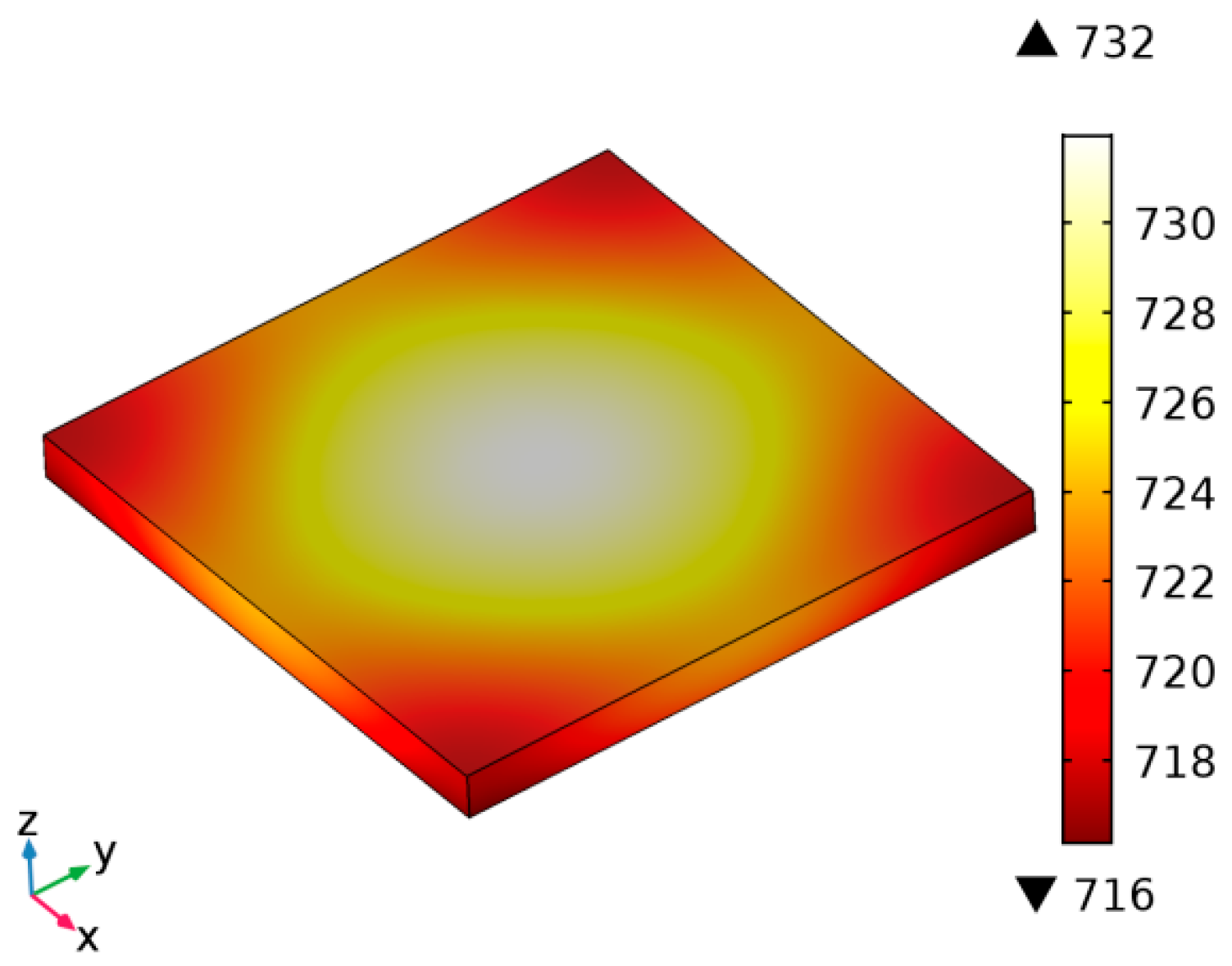
To gain a more detailed view on the spatial temperature distribution across the specimen, Figure 2 shows exemplarily the local surface temperature after irradiation with 50 W laser power for 120 s. Expectantly, in the middle of the specimen, the highest temperature was calculated, since here the maximum of the Gaussian laser beam profile impinged the surface. With locally lower laser power density and the higher surface-to-volume ratio, the coldest temperatures appeared at the samples corners. Due to the thin sample thickness, the temperature differences between the top and bottom sides were small and calculated to be about 10% of the temperature difference on the surface.
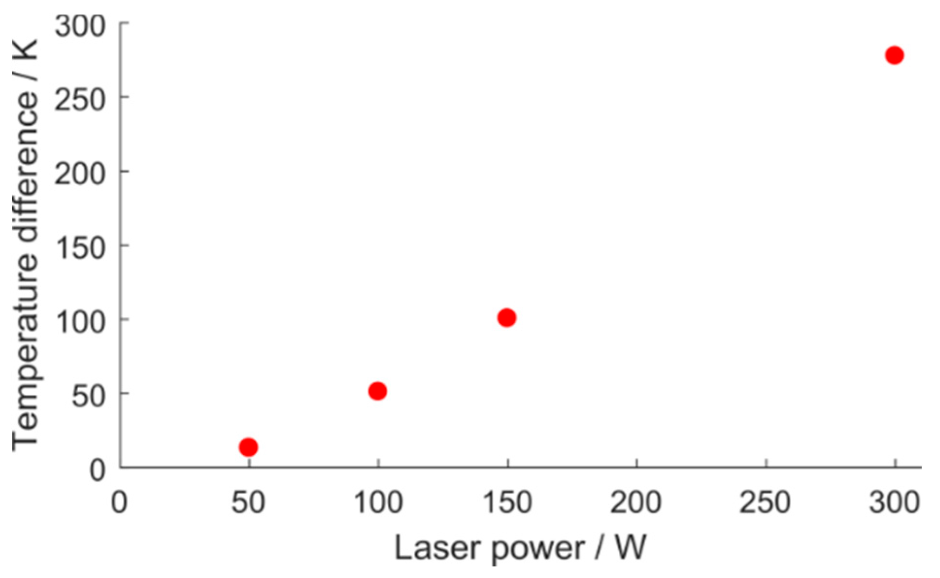
The temperature differences in the sample depended on the laser power as shown in Figure 3. With increasing laser power and therefore increasing mean temperature in the sample, the temperature differences increased. Such high temperature differences at small areas resulted in thermal induced stress.
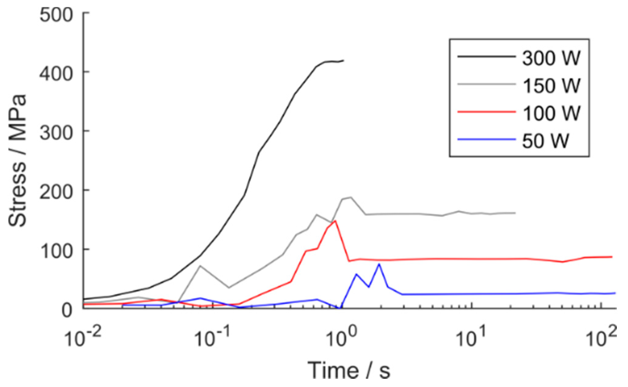
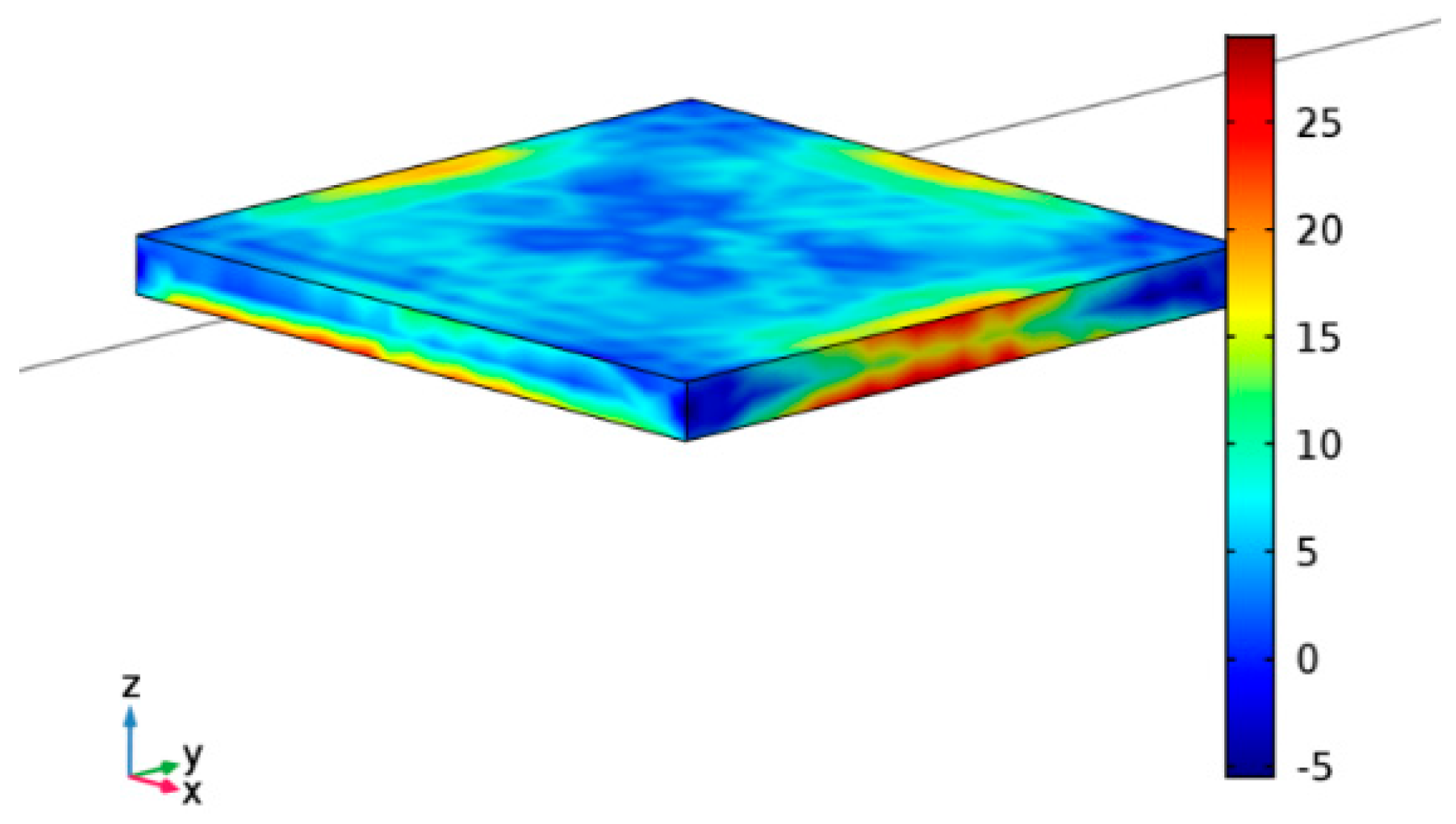
In our previous experiments, mechanical breakup was observed at intense and long lasting laser irradiation, which had been attributed to thermal induced stress. Using the above described model with the same laser powers and irradiation times as employed during the experiments, we calculated the maximum principal stress. Figure 4 depicts this stress as a function of irradiation time for different laser power levels, showing that the mechanical stress increased with both parameters in a similar way as that of the average temperature shown in Figure 1. This higher stress at higher laser power was caused by higher heating rates (cf. increased slopes in Figure 1) and higher temperature gradients across the specimen, which, in turn, resulted from the limited thermal conductivity with respect to the sample’s volume. The maximum stress occurred independently of the laser power after about 1 s irradiation followed by a decrease to a constant level. The distribution of the stress inside the specimen (Figure 4) revealed compressive stress in the middle of the sample (blue color), which was caused by higher temperatures in the middle (ref. Figure 2) and the resulting high thermal expansion. This compressive stress was countervailed by the edges where lower temperatures resulted in lower thermal expansion and therefore tensile stress, where, according to our previous experimental studies, a breakup is usually initiated.
In brittle materials like SiC, a complete breakup occurs immediately when at one location the principal stress exceeds the material strength [24]. The flexural strength of SiC is typically in the range of 365 to 424 MPa [25]. In brittle materials, the strength is characterized by a lower tensile strength as compared to the flexural strength. Because the stress in Figure 5 is mainly tensile stress, a mechanical breakup can be initiated at lower stress, as compared to the aforementioned flexural strength and is therefore highly probably at high laser power, especially at 300 W.
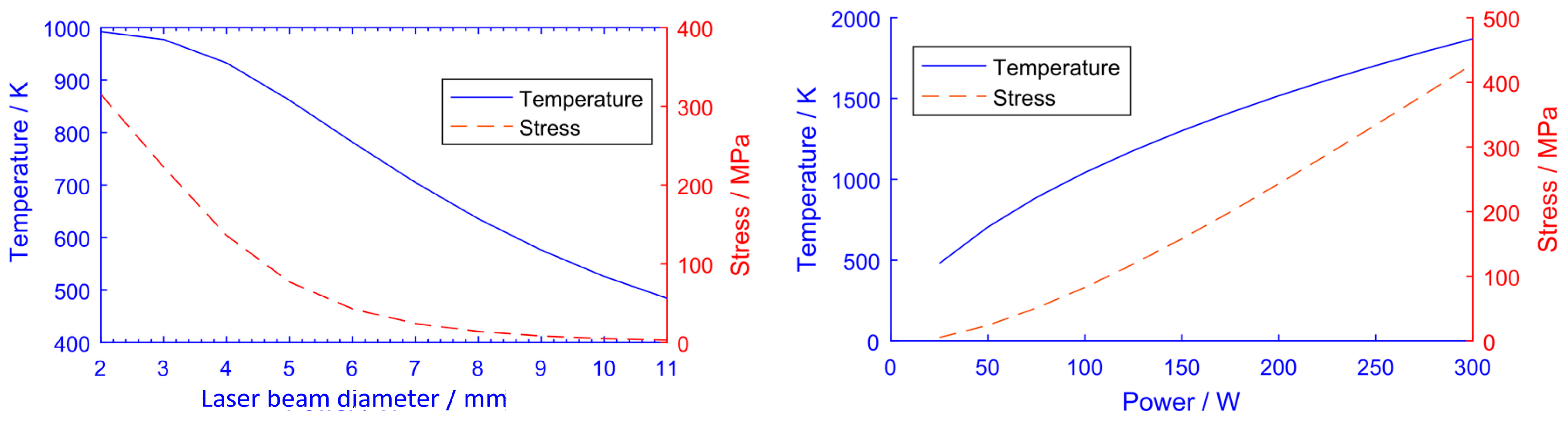
To further optimize the laser silicidation process in terms of low stress, the stress and mean temperature on the surface was simulated as a function of the laser beam diameter. The results for an irradiation time of 10 s (i.e., steady state) are shown in Figure 6 (left), revealing both lower stress and lower temperatures with increasing beam diameter. Decreasing temperature with increasing beam diameter apparently results from a decreasing proportion of the radiation impinging the SiC specimen once the laser beam is larger than the specimen (here, 4 mm). At a beam diameter below the sample size, the temperature saturates with smaller beam diameter because almost all of the laser power hits the sample (please note that the beam diameter refers to a 1/e2 decrease of the Gaussian beam intensity profile).
As a result of the lower temperatures, and due to the progressively homogeneous laser power distribution across the specimen, the thermal stress decreases as beam diameter increases. A direct comparison between stress and temperature reveals that, at a diameter below 5 mm, the descending slope of the stress is higher as compared to the temperature slope, whereas at a diameter above 8 mm the relationship changes toward a higher descending slope of the temperature, as compared to stress. In addition, larger beam diameters demand for a higher laser power to achieve a certain temperature, which is in turn required to ensure silicidation. As a consequence, a compromise between temperature and stress is required, which was, in our experimental study, a beam diameter of 7 mm.
To achieve a certain higher temperature, rather than reduce the beam diameter below 7 mm, the laser power should be varied, as shown in Figure 6 (right), because of the lower stress increase per temperature increase. For example, by increasing the temperature by 100 K from a starting point of a 7 mm beam diameter and a 50 W laser power (cf. Figure 6 left), a 15 MPa higher stress results. In contrast, a 100 K temperature increase due to a higher laser power is associated with a 19 MPa stress increase (cf. Figure 6; right) when the beam diameter decreases, so the latter is disadvantageous. Additionally, the spread between the stress increase values further increases at higher temperatures. Large beam diameters are only advantageous for irradiation with low stress at small temperatures.
4. Comparison to Experimental Results
To correlate the results of these simulations, Table 1 summarizes the experimentally achieved contact resistances for different laser powers and irradiation times, as they have been determined in our previous report [12]. The contact resistance was measured via I-V measurement with the characteristic diagram showing either a linear, ohmic behavior once silicidation was achieved or a curved characteristic line indicating unwanted nonlinear Schottky behavior. As a reference to the laser annealing, a further sample was conventionally annealed for 2 min at 1180 K in an oven. In comparison with the oven process, the simulated temperature during laser irradiation with a 50 W laser power is 720 K, i.e., significantly lower than during the RTP process. This, in turn, explains the insufficient silicidation and therefore remaining nonlinear Schottky behavior. Quite the contrary, with laser powers above 100 W, i.e., a higher achieved average temperature, ohmic contacts were achieved, and, as laser power and temperature increased, contact resistance decreased, even at shorter irradiation times. For laser powers of 150 and 300 W, the contact resistance was comparable with those achieved in conventional oven processes. However, the limit of higher laser power levels and long irradiation times is thermal induced stress, resulting in a mechanical breakup. As a compromise, for a reliable cw laser driven annealing process, 150 W for 10 s appears to be favorable for creating silicidation and ohmic contacts with competitive contact resistances.
5. Conclusions
In summary, we present here the simulation results of temperature and stress evolution during the laser-induced silicidation of ohmic contacts in 4H-SiC. In the simulation, the time-dependent temperature of the irradiated SiC sample was calculated based on the optical absorption, thermal conduction, and radiation. The calculated thermal induced stress, caused by high temperature differences, especially at high laser powers, long irradiation times, and small laser beam diameters resulted in a mechanical breakup. At simulated temperatures significantly lower than in conventional oven processes, the contacts kept their unwanted Schottky behavior, while at similar or higher temperatures a silicidation with strived-for ohmic behavior was achieved. Using the simulation, an optimized regime for laser-induced silicidation was found in terms of low contact resistance and low thermal load.
Acknowledgments
This work was funded by the German Federal Ministry of Education and Research.
Author Contributions
Benedikt Adelmann performed the simulation and experimental work. Ralf Hellmann is head of the Applied Laser and Photonics Group at the University of Aschaffenburg. Both authors discussed the results and wrote the manuscript.
Conflicts of Interest
The authors declare no conflict of interest.
References
- Ostling, M. High power devices in wide bandgap semiconductors. Sci. China 2011, 5, 1087–1093. [Google Scholar] [CrossRef]
- Mnatsakanov, T.; Pomortseva, L.; Yurkov, S. Semiempirical model of carrier mobility in silicon carbide for analyzing its dependence on temperature and doping level. Phys. Astron. 2001, 35, 394–397. [Google Scholar] [CrossRef]
- Daves, W.; Krauss, A.; Häublein, V.; Bauer, A.; Frey, L. Enhancement of the Stability of Ti and Ni Ohmic Contacts to 4H-SiC with a Stable Protective Coating for Harsh Environment Applications. J. Electr. Mater. 2011, 40, 1990–1997. [Google Scholar] [CrossRef]
- Hallin, C.; Yakimova, R.; Pecz, B.; Georgieva, A.; Marinova, T. Improved Ni Ohmic Contact on n-Type 4H-SiC. J. Electr. Mater. 1997, 26, 119–122. [Google Scholar] [CrossRef]
- Virshup, A.; Liu, F.; Lucko, D.; Buchholt, K.; Spetz, A.; Porter, L. Improved Thermal Stability Observed in Ni-Based Ohmic Contacts to n-Type SiC for High-Temperature Applications. J. Electr. Mater. 2011, 40, 400–405. [Google Scholar] [CrossRef]
- Duman, S.; Dogan, S.; Gürbulak, B.; Türüt, A. The barrier-height inhomogeneity in identically prepared Ni/n-type 6H-SiC Schottky diodes. Appl. Phys. 2008, 91, 337–340. [Google Scholar] [CrossRef]
- Tanimoto, S.; Okushi, H.; Arai, K. Ohmic Contacs for Power Devices on SiC. In Silicon Carbide; Springer: Berlin, Germany, 2004; pp. 652–658. [Google Scholar]
- Ferrero, S.; Albonico, A.; Meotto, U.; Rombola, G.; Porro, S.; Giorgis, F.; Perrone, D.; Scaltrito, L.; Bontempi, E.; Depero, L.; et al. Phase Formation at Rapid Thermal Annealing of Nickel Contacts on C-face n-type 4H-SiC. Mater. Sci. Forum 2005, 733, 483–485. [Google Scholar]
- Yoo, W.S.; Fukada, T.; Malik, I.J. Changes in Optical Properities during Nickel Silicide Formation and Potential Impact on Process Results using Various Heating Methods. Adv. Therm. Process. Semicond. 2006, 10, 243–249. [Google Scholar]
- Nakashima, K.; Eryu, O.; Ukai, S.; Yoshida, K.; Watanabe, M. Improved Ohmic Contacts to 6H-SiC by Pulsed Laser Processing. Mater. Sci. Forum 2000, 338–432, 1005–1008. [Google Scholar] [CrossRef]
- Ota, Y.; Ikeda, Y.; Kitabatake, M. Laser Alloying for Ohmic Contacs on SiC at Roop Temperature. Mater. Sci. Forum 1998, 264–268, 783–786. [Google Scholar] [CrossRef]
- Adelmann, B.; Hürner, A.; Schlegel, T.; Bauer, A.J.; Frey, L.; Hellmann, R. Laser Alloying Nickel on 4H-Silicon Carbide Substrate to Generate Ohmic Contacts. J. Laser Micro/Nanoeng. 2013, 8, 97–101. [Google Scholar] [CrossRef]
- Bell, R.O.; Toulemonde, M.; Siffert, P. Calculated temperature distribution during laser annealing in silicon and cadmium telluride. Appl. Phys. 1979, 19, 313–319. [Google Scholar] [CrossRef]
- Li, T.; Zhou, C.; Liu, Z.; Wang, W. Computational and experimental study of nanosecond laser ablation of crystalline silicon. Int. Commun. Heat Mass Transf. 2011, 38, 1041–1043. [Google Scholar] [CrossRef]
- Duc, D.H.; Naoki, I.; Kazuyoshi, F. A study of near-infrared nanosecond laser ablation of silicon carbide. Int. J. Heat Mass Transf. 2013, 65, 713–718. [Google Scholar] [CrossRef]
- Adelmann, B.; Hellmann, R. SiC absorption of near-infrared laser radiation at high temperatures. Appl. Phys. A 2016, 122, 642. [Google Scholar] [CrossRef]
- Modest, F.; Mallison, T. Transient Elastic Thermal Stress Development during Laser Scribing of Ceramics. Heat Transf. 2000, 123, 171–177. [Google Scholar] [CrossRef]
- Gomes de Mesquita, A.H. Refinement of the crystal structure of SiC type 6H. Acta Cryst. 1967, 23, 610–617. [Google Scholar] [CrossRef]
- Nilsson, O.; Mehling, H.; Horn, R.; Fricke, J.; Hofmann, R.; Muller, S.; Eckstein, R.; Hofmann, D. Determination of the thermal diffusivity and conductivity of monocrystalline silicon carbide. High Temp.-High Press. 1997, 29, 73–79. [Google Scholar] [CrossRef]
- Cooper, M.; Mikic, B.; Yovanovich, M. Thermal contact conductance. Int. J. Heat Mass Transf. 1969, 12, 279–300. [Google Scholar] [CrossRef]
- Wahid, S.M.; Madhusudana, C. Gap conductance in contact heat transfer. Int. J. Heat Mass Transf. 2000, 43, 4483–4487. [Google Scholar] [CrossRef]
- Slack, G.A.; Bartram, S.F. Thermal expansion of some diamondlike crystals. J. Appl. Phys. 1975, 46, 89–98. [Google Scholar] [CrossRef]
- Mehregany, M.; Zorman, C.A. SiC MEMS opportunities and challenges for applications in harsh environments. Thin Solid Films 1999, 355–356, 518–524. [Google Scholar] [CrossRef]
- Gross, D.; Seelig, T. Fracture Mechanics; Ling, F., Ed.; Springer: Berlin, Germany, 2006. [Google Scholar]
- Snead, L.L.; Nozawa, T.; Katoh, Y.; Byun, T.; Kondo, S.; Petti, D.A. Handbook of SiC properties for fuel performance modeling. J. Nucl. Mater. 2007, 371, 329–377. [Google Scholar] [CrossRef]
Figure 1.
Simulated mean temperature on the surface of the SiC samples as a function of irradiation time and laser power.
Figure 1.
Simulated mean temperature on the surface of the SiC samples as a function of irradiation time and laser power.
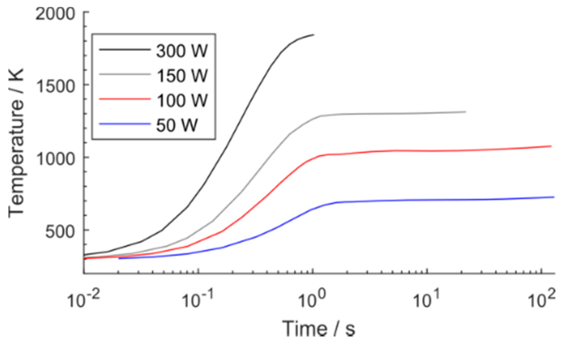
Figure 2.
The temperature distribution of an SiC sample placed on a steel sheet irradiated with 50 W laser power for 120 s.
Figure 2.
The temperature distribution of an SiC sample placed on a steel sheet irradiated with 50 W laser power for 120 s.

Figure 3.
Temperature differences inside the SiC specimen at 1 s irradiation time as function of laser power.
Figure 3.
Temperature differences inside the SiC specimen at 1 s irradiation time as function of laser power.

Figure 4.
Maximum thermal induced stress (principal stress) as a function of laser power and irradiation time.
Figure 4.
Maximum thermal induced stress (principal stress) as a function of laser power and irradiation time.

Figure 5.
Stress distribution after 120 s at 50 W with the red color indicating tensile stress and the blue color compressive stress.
Figure 5.
Stress distribution after 120 s at 50 W with the red color indicating tensile stress and the blue color compressive stress.

Figure 6.
Simulated temperature and stress after 10 s irradiation as a function of laser beam diameter for a 50 W laser power (left) and laser power at a 7 mm beam diameter (right).
Figure 6.
Simulated temperature and stress after 10 s irradiation as a function of laser beam diameter for a 50 W laser power (left) and laser power at a 7 mm beam diameter (right).


Table 1.
Overview of irradiation results.
| Power | Time | Temperature | Contact Resistance |
|---|---|---|---|
| W | s | K | |
| 50 | 30 | 716 | not linear |
| 50 | 120 | 720 | not linear |
| 100 | 30 | 1050 | 37 |
| 100 | 120 | 1070 | 10 |
| 150 | 10 | 1300 | 4.3 |
| 300 | 0.5 | 1630 | 1.4 |
| Oven | 120 | 1180 | 2.5 |
© 2017 by the authors. Licensee MDPI, Basel, Switzerland. This article is an open access article distributed under the terms and conditions of the Creative Commons Attribution (CC BY) license (http://creativecommons.org/licenses/by/4.0/).
Share and Cite
MDPI and ACS Style
Adelmann, B.; Hellmann, R. Temperature and Stress Simulation of 4H-SiC during Laser-Induced Silicidation for Ohmic Contact Generation. Metals 2017, 7, 545. https://doi.org/10.3390/met7120545
AMA Style
Adelmann B, Hellmann R. Temperature and Stress Simulation of 4H-SiC during Laser-Induced Silicidation for Ohmic Contact Generation. Metals. 2017; 7(12):545. https://doi.org/10.3390/met7120545
Chicago/Turabian StyleAdelmann, Benedikt, and Ralf Hellmann. 2017. "Temperature and Stress Simulation of 4H-SiC during Laser-Induced Silicidation for Ohmic Contact Generation" Metals 7, no. 12: 545. https://doi.org/10.3390/met7120545
Note that from the first issue of 2016, this journal uses article numbers instead of page numbers. See further details here.