Article

Synthesis of Cascadable DDCC-Based Universal Filter Using NAM

1
Department of Electronic Engineering, National Kaohsiung University of Applied Sciences, Kaohsiung 807, Taiwan
2
Department of Physics, University of Dalat, Dalat City, Vietnam
3
Department of Electronic Engineering, Kun Shan University, Tainan 710, Taiwan
*
Author to whom correspondence should be addressed.
Appl. Sci. 2015, 5(3), 320-343; https://doi.org/10.3390/app5030320
Submission received: 9 July 2015 / Revised: 2 August 2015 / Accepted: 4 August 2015 / Published: 11 August 2015
(This article belongs to the Special Issue Feature Papers)

Abstract

:
A novel systematic approach for synthesizing DDCC-based voltage-mode biquadratic universal filters is proposed. The DDCCs are described by infinity-variables’ models of nullor-mirror elements which can be used in the nodal admittance matrix expansion process. Applying the proposed method, the obtained 12 equivalent filters offer the following features: multi-input and two outputs, realization of all five standard filter functions, namely lowpass, bandpass, highpass, notch and allpass, high-input impedance, employing only grounded capacitors and resistors, orthogonal controllability between pole frequency and quality factor, and cascadable, low active and passive sensitivities. The workability of some synthesized filters is verified by HSPICE simulations to demonstrate the feasibility of the proposed method.

1. Introduction

Due to the capability to realize simultaneously multiple filter functions with the same topology, continued researches have focused on the realization of universal filters. The design of biquadratic voltage-mode active filters with high-input impedance has received much interest since they can be directly cascaded to implement higher order filters without the use of additional buffer circuits [1]. Many voltage-mode universal biquadratic filters using current conveyors with multi-input/multi-output were proposed in the literature [2,3,4,5,6,7,8,9,10].
Recently, a symbolic framework for systematic synthesis of a linear active circuit without any detailed prior knowledge of the circuit form was presented [11,12,13,14,15]. This method, called nodal admittance matrix (NAM) expansion, is very useful to generate various novel circuits in a systematic way. Based on this method, various active networks such as filters, oscillators and gyrators employing OTA, CCII, BOCCII, DVCC and CCCCTA have been synthesized [16,17,18,19,20,21]. The circuit synthesis procedure proposed in [12] is suitable to synthesize discrete transfer functions with different circuit topologies. It is difficult to synthesize multiple filter functions using an identical topology. The systematic generation of current-mode filters using NAM expansion was reported in [16]. The trans-impedance filter synthesis based on NAM expansion was reported in [17]. In [19], the synthesis of CCII-based voltage-mode high-Q biquadratic notch filter was reported recently.
Since the differential difference current conveyor (DDCC) is a circuit similar to a DDA at the input side and a CCII at the output side [22], it enjoys the combined advantages of the CCII and DDA with high-input impedance, low-output impedance, greater design flexibility, larger signal bandwidth and wider current dynamic range, several universal filters using DDCCs have been proposed [23,24,25,26]. Unfortunately, most papers just propose their novel circuits; the design or synthesis methods for DDCC-based universal filters are not available.
In this paper, a systematic generation of cascadable DDCC-based universal voltage-mode biquadratic filters is presented. The obtained 12 filters configurations with two outputs can be used to realize all the five generic filter functions. They comprise three active elements and five passive grounded capacitors and resistors, with the features of high input impedance, low active and passive sensitivities, and orthogonal adjustability of the resonance angular frequency and quality factor. The filter with grounded capacitors is helpful for easing the elimination/accommodation of various parasitic effects for monolithic integration. HSPICE simulations for two illustrated derived filters confirm the workability of the obtained circuits, and hence demonstrate the feasibility of the proposed approach.

2. Description of the Proposed Method

The port relations of an ideal DDCC can be characterized by (1), where the plus and minus signs indicate whether the current conveyor is DDCC+ or DDCC−. Figure 1 shows the symbolic pathological representations of DDCCs. It is clear that each of terminal-Yi (i = 1–3) possesses high input impedance.
[ V X I Y 1 I Y 2 I Y 3 I Z ] = [ 1 1 1 0 0 0 0 0 0 0 0 0 0 0 0 0 0 0 0 ± 1 ] [ V Y 1 V Y 2 V Y 3 I X ]
Figure 1. The symbolic pathological representations of DDCCs.
Applsci 05 00320 g001
In the NAM expansion process, the addition of row and column of zero terms and infinity-variable terms with a common node on the primary diagonal of the admittance matrix is needed to transform the admittance terms to their correct form. The correct form set of admittance terms includes a unique positive term on the primary diagonal realizing a grounded admittance and a group of four terms with two positive terms on the primary diagonal and two negative terms on the off-diagonal representing a floating admittance. Therefore, in the synthesized circuits, pairs of pathological elements with a common node can be realized by the proper type of CCIIs [19].
The DDCC is similar to a CCII but with two more additional terminals, i.e., terminal-Y2 and terminal-Y3. Thus, the DDCC- and DDCC+ can be respectively represented by infinity-variables notation given by Equations (2) and (3) in NAM expansion with the common node on the primary diagonal assigned to terminal-X. The signs of infinity-variables of terminal-Y1 and terminal-Y3 are different to that of terminal-X, while the signs of infinity-variables of terminal-X and terminal-Y2 are identical. Based on the infinity-variables notation in (2) and (3), it can be seen that the connection between terminal-X and terminal-Y1 or terminal-Y3 corresponds to a nullator, and the connection between terminal-X and terminal-Y2 corresponds to a voltage-mirror (VM). These relationships are very important for deriving the numerator of the transfer function of the synthesized filters.
     Y 3        Y 2        Y 1 X [ i i i i i i i i ] X Z
Y 3 Y 2 Y 1 X [ i i i i i i i i ] X Z +
It is known that to synthesize filter circuits using NAM expansion, the denominator D(s) of a transfer function of a filter should be expressed as an admittance matrix in NAM equations shown in Equation (4). This matrix can be used as a starting matrix to find the circuit configuration with no input signals. Then, the equivalent circuit of an input voltage source as shown in Figure 2 can be injected to the obtained circuit represented by expanded NAM of (4) to obtain the voltage-mode filters [19].
[ y 1 , 1 y 1 , 2 y 1 , j y 1 , n y 2 , 1 y 2 , 2 y 2 , j y 2 , n y i , 1 y i , 2 y i , j y i , n y n , 1 y n , 2 y n , j y n , n ]
Figure 2. R-nullor equivalent circuit of a voltage source.
Applsci 05 00320 g002
To synthesize DDCC-grounded capacitor-based filters using NAM expansion, we firstly use the NAM stamps of CCIIs [15] to expand the starting matrix in (4). The expanded NAM of (4) includes the correct form of admittance elements and pairs of infinity-variables represented terminal-X, terminal-Z and one terminal-Yi of DDCCs. The remained Yi-terminals can be used to inject the input voltage source for deriving high input impedance filters. The procedure can be summarized as follows.
Step 1:
Of the desired transfer function of the synthesized filter in the form of the Matrix (4). It must be noted that each capacitor in the denominator must be arranged to have only a single position on the primary diagonal to obtain circuits with grounded capacitors.
Step 2:
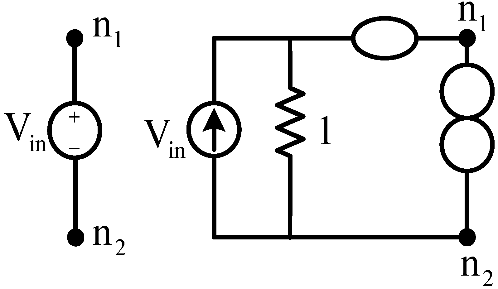
Introduce a row and a column of zeros to row 1 and column 1 and place a unity resistor to position (1,1) of (4). The existing columns and rows are moved to the right and to the bottom, as given by (5). Then add infinity variables and zero terms to realize a nullator between column 1 and column 2 and a norator between row 2 and ground. The Step 2 corresponds to the adding of the equivalent circuit of voltage source in Figure 2 [19]. So, Matrix (5) becomes (6).
[ 1 0 0 0 0 0 0 0 y 1 , 1 y 1 , 2 y 1 , j y 1 , n 0 y 2 , 1 y 2 , 2 y 2 , j y 2 , n 0 y i , 1 y i , 2 y i , j y i , n 0 y n , 1 y n , 2 y n , j y n , n ]
[ 1 0 0 0 0 0 0 0 1 1 0 0 0 0 0 0 0 0 y 1 , 1 y 1 , 2 y 1 , j y 1 , n 0 0 y 2 , 1 y 2 , 2 y 2 , j y 2 , n 0 0 y i , 1 y i , 2 y i , j y 2 , n 0 0 y n , 1 y n , 2 y n , j y n , n ]
Step 3:
Use the NAM expansion method to expand the Matrix (6) [12,15]. The obtained matrix can be expressed by (7), for example.
[ 1 0 0 0 0 0 0 0 0 1 1 0 0 0 0 0 0 0 0 0 y 1 , 1 i y 1 , j y 1 , n i 0 0 y 2 , 1 y 2 , 2 y 2 , j y 2 , n 0 0 0 y i , 1 y i , 2 y i , j y i , n 0 0 0 y n , 1 y n , 2 y n , j y n , n 0 0 0 0 i 0 0 0 0 y 1 , 2 + i ]
Step 4:
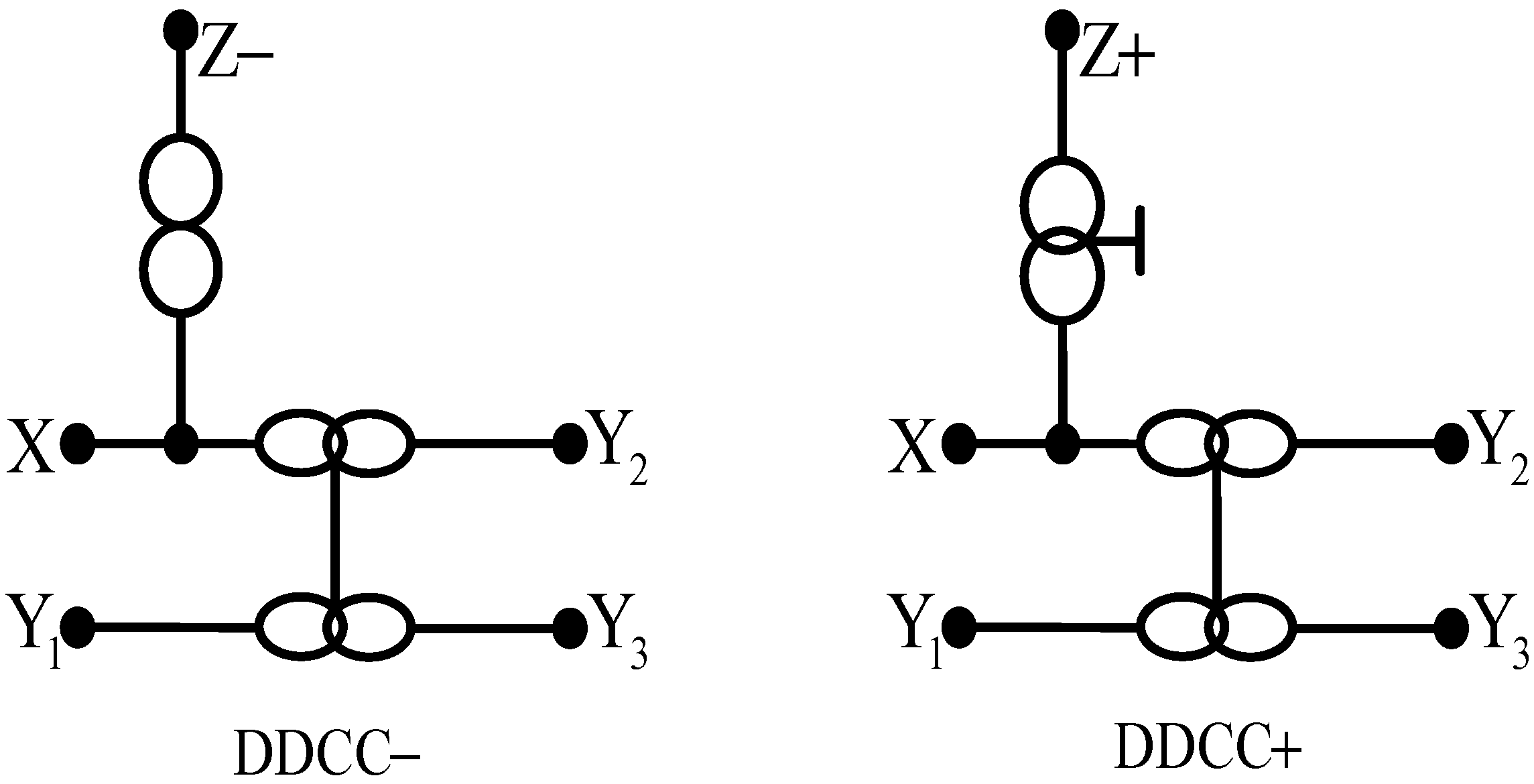
Add pair of infinity-variables of remained Yi-terminals represented by (2) or (3) to the suitable positions in column 2 of the Matrix (7) to realize the infinity-variables notation of a DDCC+ or DDCC−. This operation will duplicate the existing admittance terms to the first column of (5), so the numerator of the desired transfer function is obtained. For example, by adding a pair of ± ∞i to the second column of (7), the term y1,2 will be duplicated in the first column of (5) to obtain the desired numerator, as shown in (8). The addition of infinity-variable pairs to column 2 corresponds to applying input voltage signal to the added Yi-terminals at node 2. This operation will not affect the denominator of the transfer function. The obtained matrix represents the full matrix of the synthesized circuit.
[ 1 0 0 0 0 0 0 0 0 1 1 0 0 0 0 0 0 0 0 ± i y 1 , 1 i y 1 , j y 1 , n i 0 0 y 2 , 1 y 2 , 2 y 2 , j y 2 , n 0 0 0 y i , 1 y i , 2 y i , j y i , n 0 0 0 y n , 1 y n , 2 y n , j y n , n 0 0 ± i 0 i 0 0 0 0 y 1 , 2 + i ]
It can be observed that in the starting Matrix (5), the node 1 is chosen as input voltage node and other nodes can be output nodes. In (6), the node 1 and node 2 are connected by a nullator then they are equivalent to the input node, and other nodes can be output nodes. In Step 4, each pair of infinity-variables added to the second column of the obtained matrix in Step 3 corresponds to the injecting of input voltage signal to one Y-terminal of DDCCs. So, the circuits with high input impedance and multi-input and multi-output properties can therefore be synthesized.

3. Application Examples

We hope to synthesize biquadratic voltage-mode universal filters using a minimum number of passive elements with independent adjustable parameters of Q factor and pole frequency. The denominator of the transfer function is chosen as (9).
D ( s ) = s 2 C 1 C 2 + s C 2 G 1 + G 2 G 3
According to the procedure of Step 1 in Section 2, the Equation (9) is expressed by (10) and (11) in the form of (4).
[ G 1 + s C 1 G 2 G 3 s C 2 ]
[ G 1 + s C 1 G 2 G 3 s C 2 ]
The Matrices (10) and (11) are defined as NAM type-A and NAM type-B, respectively. They are used as the starting matrices in NAM expansion.

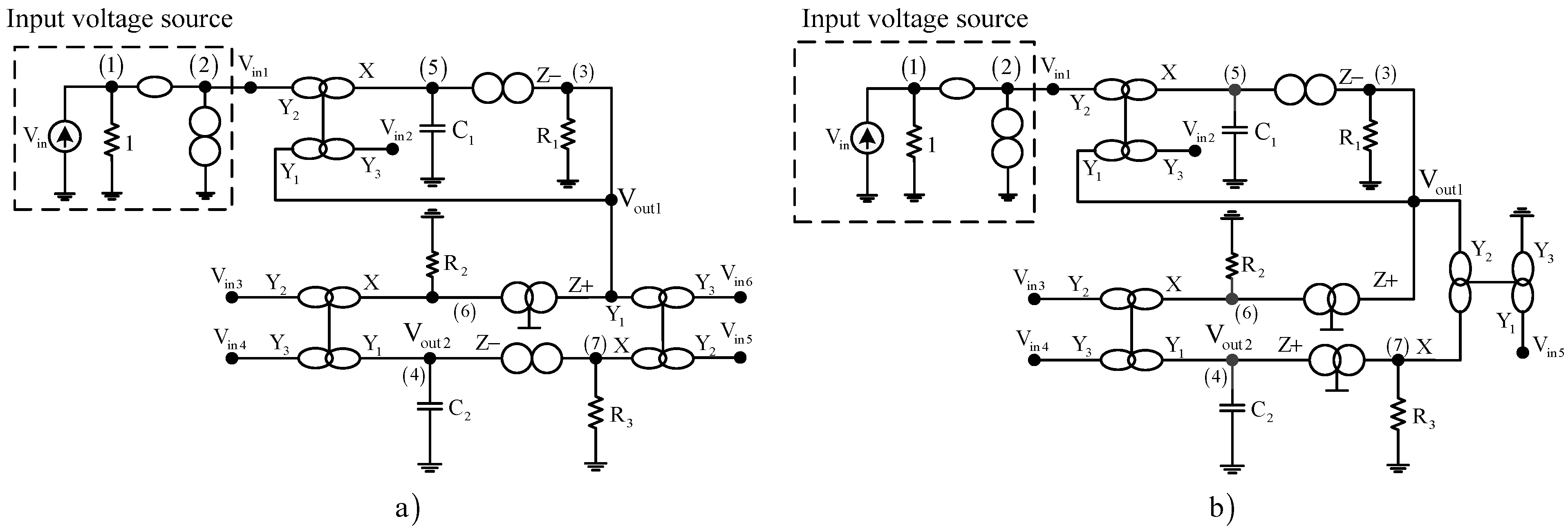
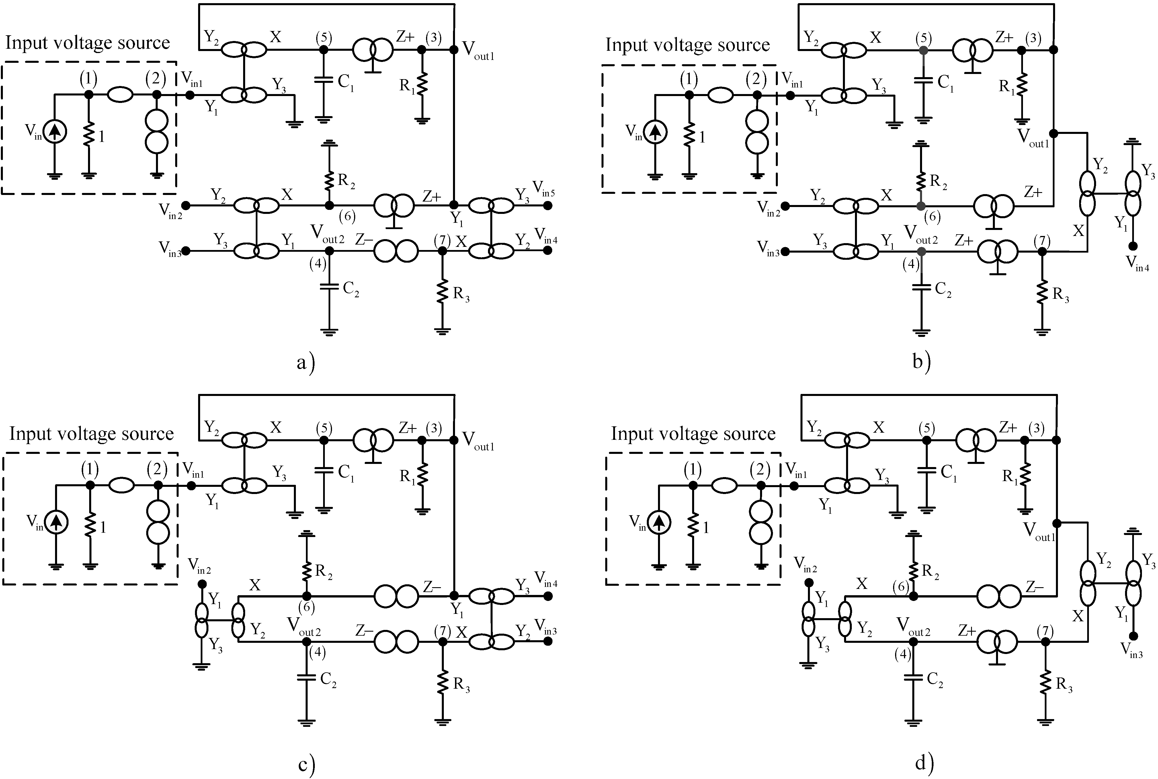
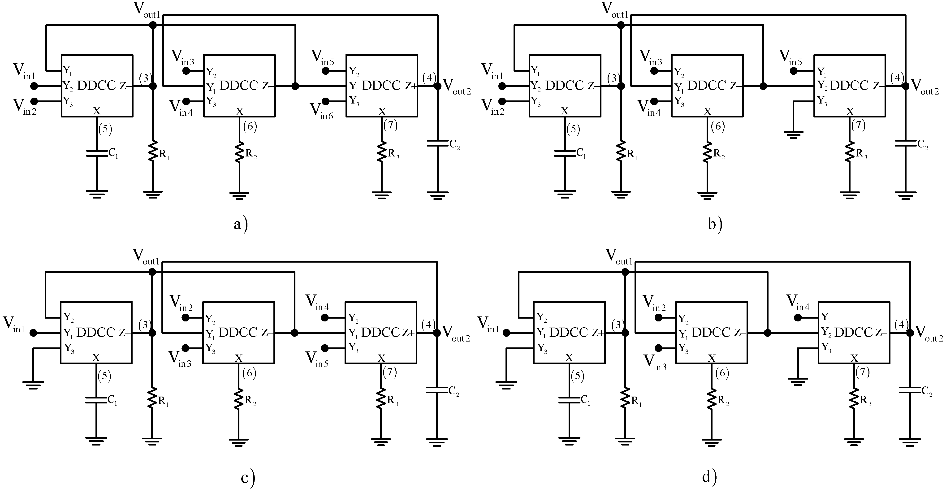
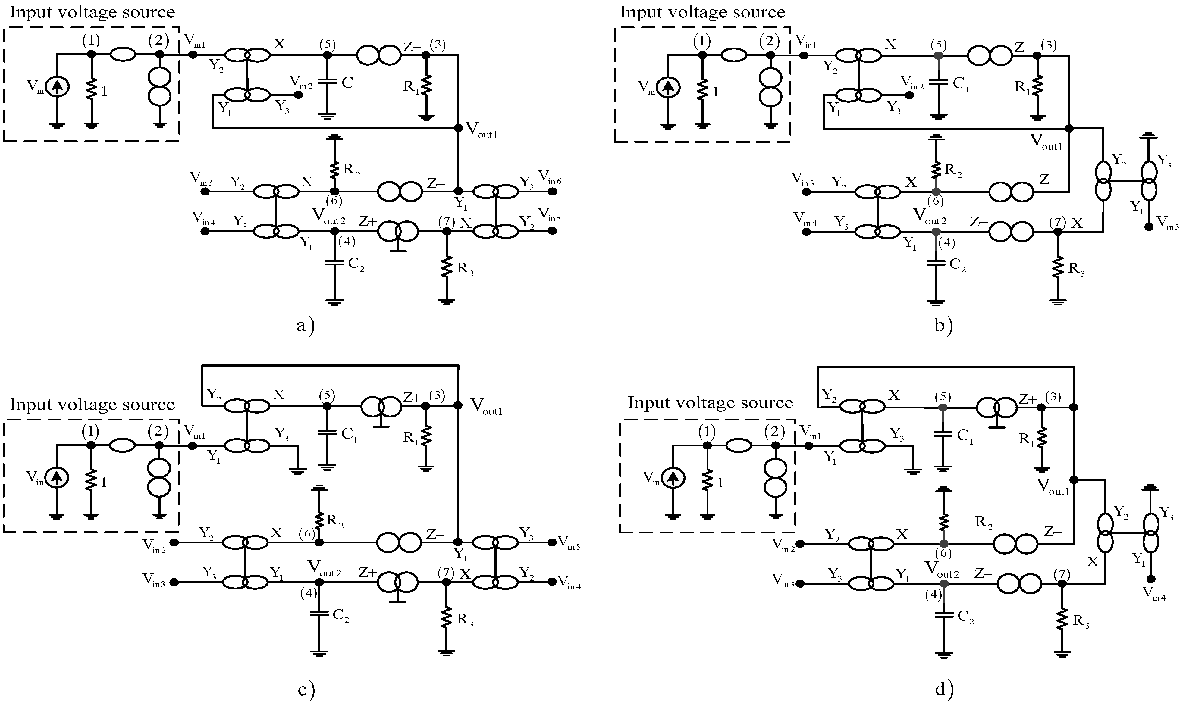
3.1. Synthesis of Type-A Universal Filters

Following Step 2 of the procedure in Section 2, the equivalent NAMs (12) and (13) are obtained from (10). In the Matrix (12), the node 1 is chosen as input node, nodes 2 and 3 are chosen as outputs, respectively denoted by Vou1 and Vout2. In (13), the output voltage nodes Vout1 and Vout2 are moved to node 3 and 4, respectively.
[ 1 0 0 0 G 1 + s C 1 G 2 0 G 3 s C 2 ]
[ 1 0 0 0 1 1 0 0 0 0 G 1 + s C 1 G 2 0 0 G 3 s C 2 ]
Using Step 3, three columns and rows of zero terms are added and pairs of nullor-mirror elements represented by ∞2, ∞3 and ∞4 are introduced to the right and bottom of Matrix (13). So, Matrix (13) can be expanded as (14). There are eight alternative cases (cases 1–8) in expanding the Matrix (13), as shown in Table 1.
[ 1 0 0 0 0 0 0 1 1 0 0 0 0 0 0 0 G 1 + 2 3 2 3 0 0 0 4 s C 2 0 0 4 0 0 2 0 s C 1 + 2 0 0 0 0 0 3 0 G 2 + 3 0 0 0 4 0 0 0 G 3 + 4 ]
In (14), the DDCC(1), DDCC(2) and DDCC(3) are represented by terms ±∞2, ±∞3 and ±∞4, respectively. Based on the NAM stamps in (2) and (3) and the common node on the primary diagonal assigned for terminal-X of a DDCC, the terminal-X of DDCC(1) can be node 5, terminal-Y1 and terminal-Z (of minus-type DDCC) are connected to node 3. For the DDCC(2), the terminal-X is connected to node 6, terminal-Y1 is connected to node 4 and terminal-Z (plus-type DDCC) is connected to node 3. For the DDCC(3), the terminal-X is connected to node 7, terminal-Y1 is connected to node 3 and terminal-Z (minus type DDCC) is connected to node 4. All of the terminal-Y2 and terminal-Y3 of DDCC(1), DDCC(2) and DDCC(3) can be used to inject the input voltage source.
Using Step 4, by injecting the input voltage source into terminal-Y2 of DDCC(1), the term –sC1 will be added to position (2,1) of (12), then a highpass function at Vout1 and bandpass function at Vout2 can be obtained. This operation corresponds to the inserting of term ±∞2 to the second column of (14), as shown in (15). The obtained filter represented by (15) is shown in Figure 3a with nodes Vin2, Vin3, Vin4, Vin5 and Vin6 being grounded.
By applying the input voltage source to terminal-Y3 of DDCC(1), the term sC1 will be also created in position (2,1) of (12). Therefore, the admittance matrix is shown in (16) and the obtained transfer functions at nodes Vout1 and Vout2 are identical to that obtained in (15) but with reverse signs. The derived circuit is shown in Figure 3a with moving the injected voltage source equivalent circuit to node Vin2 and grounding nodes Vin1, Vin3, Vin4, Vin5 and Vin6.
Table 1. Eight cases of expanding NAM Type-A.
NAM Type-A (Case 1)NAM Type-A (Case 2)
[ 1 0 0 0 0 0 0 1 1 0 0 0 0 0 0 0 G 1 + 2 3 2 3 0 0 0 4 s C 2 0 0 4 0 0 2 0 s C 1 + 2 0 0 0 0 0 3 0 G 2 + 3 0 0 0 4 0 0 0 G 3 + 4 ] [ 1 0 0 0 0 0 0 1 1 0 0 0 0 0 0 0 G 1 + 2 3 2 3 0 0 0 4 s C 2 0 0 4 0 0 2 0 s C 1 + 2 0 0 0 0 0 3 0 G 2 + 3 0 0 0 4 0 0 0 G 3 + 4 ]
NAM Type-A (Case 3)NAM Type-A (Case 4)
[ 1 0 0 0 0 0 0 1 1 0 0 0 0 0 0 0 G 1 + 2 3 2 3 0 0 0 4 s C 2 0 0 4 0 0 2 0 s C 1 + 2 0 0 0 0 0 3 0 G 2 + 3 0 0 0 4 0 0 0 G 3 + 4 ] [ 1 0 0 0 0 0 0 1 1 0 0 0 0 0 0 0 G 1 + 2 3 2 3 0 0 0 4 s C 2 0 0 4 0 0 2 0 s C 1 + 2 0 0 0 0 0 3 0 G 2 + 3 0 0 0 4 0 0 0 G 3 + 4 ]
NAM Type-A (Case 5)NAM Type-A (Case 6)
[ 1 0 0 0 0 0 0 1 1 0 0 0 0 0 0 0 G 1 + 2 3 2 3 0 0 0 4 s C 2 0 0 4 0 0 2 0 s C 1 + 2 0 0 0 0 0 3 0 G 2 + 3 0 0 0 4 0 0 0 G 3 + 4 ] [ 1 0 0 0 0 0 0 1 1 0 0 0 0 0 0 0 G 1 + 2 3 2 3 0 0 0 4 s C 2 0 0 4 0 0 2 0 s C 1 + 2 0 0 0 0 0 3 0 G 2 + 3 0 0 0 4 0 0 0 G 3 + 4 ]
NAM Type-A (Case 7)NAM Type-A (Case 8)
[ 1 0 0 0 0 0 0 1 1 0 0 0 0 0 0 0 G 1 + 2 3 2 3 0 0 0 4 s C 2 0 0 4 0 0 2 0 s C 1 + 2 0 0 0 0 0 3 0 G 2 + 3 0 0 0 4 0 0 0 G 3 + 4 ] [ 1 0 0 0 0 0 0 1 1 0 0 0 0 0 0 0 G 1 + 2 3 2 3 0 0 0 4 s C 2 0 0 4 0 0 2 0 s C 1 + 2 0 0 0 0 0 3 0 G 2 + 3 0 0 0 4 0 0 0 G 3 + 4 ]
Figure 3. The pathological representations of derived type-A filters (cases 1–4).
Applsci 05 00320 g003aApplsci 05 00320 g003b
[ 1 0 0 0 0 0 0 1 1 0 0 0 0 0 0 2 G 1 + 2 3 2 3 0 0 0 4 s C 2 0 0 4 0 2 2 0 s C 1 + 2 0 0 0 0 0 3 0 G 2 + 3 0 0 0 4 0 0 0 G 3 + 4 ]
[ 1 0 0 0 0 0 0 1 1 0 0 0 0 0 0 2 G 1 + 2 3 2 3 0 0 0 4 s C 2 0 0 4 0 2 2 0 s C 1 + 2 0 0 0 0 0 3 0 G 2 + 3 0 0 0 4 0 0 0 G 3 + 4 ]
Similarly, by applying the input voltage source to terminal-Y2 of DDCC(2), term G2 will appear in the position (2,1) of (12), then a bandpass function at Vout1 and a lowpass function at Vout2 can be obtained. The admittance matrix can be given in (17) and the derived circuit is shown in Figure 3a with moving the injected voltage source to node Vin3 and grounding nodes Vin1, Vin2, Vin4, Vin5 and Vin6.
[ 1 0 0 0 0 0 0 1 1 0 0 0 0 0 0 3 G 1 + 2 3 2 3 0 0 0 4 s C 2 0 0 4 0 0 2 0 s C 1 + 2 0 0 0 3 0 3 0 G 2 + 3 0 0 0 4 0 0 0 G 3 + 4 ]
By applying the input voltage source to terminal-Y3 of DDCC(2), the term –G2 will appear in position (2,1) of (12), then we can obtain the admittance matrix in (18) and the filter with identical transfer functions as (17) but with different signs at nodes Vout1 and Vout2. For the circuit in Figure 3a, moving the injected voltage source equivalent circuit to node Vin4 with nodes Vin1, Vin2, Vin3, Vin5 and Vin6 as grounded nodes, we can obtain the filter represented by (18).
[ 1 0 0 0 0 0 0 1 1 0 0 0 0 0 0 3 G 1 + 2 3 2 3 0 0 0 4 s C 2 0 0 4 0 0 2 0 s C 1 + 2 0 0 0 3 0 3 0 G 2 + 3 0 0 0 4 0 0 0 G 3 + 4 ]
Also, a lowpass function at Vout1 can be achieved by applying the input voltage source to terminal-Y2 of DDCC(3) when the term –G3 appear in position (3,1) of (12). This operation corresponds to the inserting of terms ±∞4 to the second column of (14), as shown in (19). The obtained circuit is shown in Figure 3a by moving the injected voltage source to node Vin5 with nodes Vin1, Vin2, Vin3, Vin4 and Vin6 being grounded.
[ 1 0 0 0 0 0 0 1 1 0 0 0 0 0 0 0 G 1 + 2 3 2 3 0 0 4 4 s C 2 0 0 4 0 0 2 0 s C 1 + 2 0 0 0 0 0 3 0 G 2 + 3 0 0 4 4 0 0 0 G 3 + 4 ]
By applying the input voltage source to terminal-Y3 of DDCC(3), term G3 will arise in position (3,1) of (12), then the obtained transfer function at node Vout1 is identical to the circuit represented by (19) with reverse sign. Its admittance matrix is shown in (20) and the circuit is given in Figure 3a by moving the injected voltage source to node Vin6 with nodes Vin1, Vin2, Vin3, Vin4 and Vin5 being grounded.
[ 1 0 0 0 0 0 0 1 1 0 0 0 0 0 0 0 G 1 + 2 3 2 3 0 0 4 4 s C 2 0 0 4 0 0 2 0 s C 1 + 2 0 0 0 0 0 3 0 G 2 + 3 0 0 4 4 0 0 0 G 3 + 4 ]
In addition, a notch function at Vout1 can be achieved by applying the input voltage source to terminal-Y2 of DDCC(1) and terminal-Y2 of DDCC(3) when the terms –sC1 and –G3 arise in positions (2, 1) and (3, 1) of (12), respectively. This operation corresponds to the inserting of terms ±∞2 and ±∞4 to the second column of (14), as shown in (21). The obtained circuit is given in Figure 3a by moving the injected voltage source to the merged node of Vin1 and Vin5 with nodes Vin2, Vin3, Vin4 and Vin6 being grounded. Another notch function at Vout1 can be also obtained by injecting the input voltage source to the merged node of Vin2 and Vin6 in Figure 3a with nodes Vin1, Vin3, Vin4 and Vin5 being grounded.
[ 1 0 0 0 0 0 0 1 1 0 0 0 0 0 0 2 G 1 + 2 3 2 3 0 0 4 4 s C 2 0 0 4 0 2 2 0 s C 1 + 2 0 0 0 0 0 3 0 G 2 + 3 0 0 4 4 0 0 0 G 3 + 4 ]
Applying the input voltage source to terminal-Y2 of DDCC(1), terminal-Y2 of DDCC(2) and terminal-Y2 of DDCC(3), terms –sC1+G2 and –G3 will be created in positions (2, 1) and (3, 1) of (12), respectively, then an allpass function at Vout1 (with G2 = G1) can be achieved. This operation corresponds to the insertion of the terms ±∞2, ∞3 and ±∞4 to the second column of (14) as shown in (22). In Figure 3a, moving the injected voltage source to the merged node of Vin1, Vin3 and Vin5 with nodes Vin2, Vin4 and Vin6 being grounded, we can obtain the filter represented by (22). Another allpass function at Vout1 can be also obtained by injecting the input voltage source to the merged node of Vin2, Vin4 and Vin6 in Figure 3a with nodes Vin1, Vin3, and Vin5 being grounded.
[ 1 0 0 0 0 0 0 1 1 0 0 0 0 0 0 2 + 3 G 1 + 2 3 2 3 0 0 4 4 s C 2 0 0 4 0 2 2 0 s C 1 + 2 0 0 0 3 0 3 0 G 2 + 3 0 0 4 4 0 0 0 G 3 + 4 ]
In the same way, the synthesized procedure can be applied to the matrices for cases 2–8 in Table 1. Four equivalent circuits of the derived filters for cases 1–4 of derived type-A filters in Table 1 are shown in Figure 3. The output transfer functions of the synthesized circuits for case 1 are given by (23) and (24). Besides, four equivalent circuits of the synthesized filters for cases 5–8 of derived type-A filters in Table 1 are shown in Figure 4. The output transfer functions of the synthesized circuits for case 5 are given by (25) and (26). Figure 5a–d and e–h show the practical configurations for the pathological equivalents in Figure 3 and Figure 4, respectively.
V out 1 = s 2 C 1 C 2 V in1 s 2 C 1 C 2 V in 2 s C 2 G 2 V in 3 + s C 2 G 2 V in 4 + G 2 G 3 V in 5 G 2 G 3 V in 6 s 2 C 1 C 2 + s C 2 G 1 + G 2 G 3
V out 2 = s C 1 G 3 V in1 + s C 1 G 3 V in 2 + G 2 G 3 V in 3 G 2 G 3 V in 4 + G 3 ( G 1 + s C 1 ) V in 5 G 3 ( G 1 + s C 1 ) V in 6 s 2 C 1 C 2 + s C 2 G 1 + G 2 G 3
V out 1 = s 2 C 1 C 2 V in1 s C 2 G 2 V in 2 + s C 2 G 2 V in 3 + G 2 G 3 V in 4 G 2 G 3 V in 5 s 2 C 1 C 2 + s C 2 G 1 + G 2 G 3
V out 2 = s C 1 G 3 V in1 + G 2 G 3 V in 2 G 2 G 3 V in 3 + G 3 ( G 1 + s C 1 ) V in 4 G 3 ( G 1 + s C 1 ) V in 5 s 2 C 1 C 2 + s C 2 G 1 + G 2 G 3
Figure 4. The pathological representations of derived type-A filters (cases 5–8).
Applsci 05 00320 g004
Figure 5. The practical configuration of type-A filters.
Applsci 05 00320 g005aApplsci 05 00320 g005b

3.2. Synthesis of Type-B Universal Filters

Similarly, by applying Step 2, the equivalent NAMs (27) and (28) are obtained from (11). Applying Step 3, the Matrix (28) can be expanded as (29). There are four alternative cases (cases 1–4) that can be derived by expanding Matrix (28), as shown in Table 2.
[ 1 0 0 0 G 1 + s C 1 G 2 0 G 3 s C 2 ]
[ 1 0 0 0 1 1 0 0 0 0 G 1 + s C 1 G 2 0 0 G 3 s C 2 ]
[ 1 0 0 0 0 0 0 1 1 0 0 0 0 0 0 0 G 1 + 2 3 2 3 0 0 0 4 s C 2 0 0 4 0 0 2 0 s C 1 + 2 0 0 0 0 0 3 0 G 2 + 3 0 0 0 4 0 0 0 G 3 + 4 ]
Table 2. Four cases of expanding NAM Type-B.
NAM Type-B (Case 1)NAM Type-B (Case 2)
[ 1 0 0 0 0 0 0 1 1 0 0 0 0 0 0 0 G 1 + 2 3 2 3 0 0 0 4 s C 2 0 0 4 0 0 2 0 s C 1 + 2 0 0 0 0 0 3 0 G 2 + 3 0 0 0 4 0 0 0 G 3 + 4 ] [ 1 0 0 0 0 0 0 1 1 0 0 0 0 0 0 0 G 1 + 2 3 2 3 0 0 0 4 s C 2 0 0 4 0 0 2 0 s C 1 + 2 0 0 0 0 0 3 0 G 2 + 3 0 0 0 4 0 0 0 G 3 + 4 ]
NAM Type-B (Case 3)NAM Type-B (Case 4)
[ 1 0 0 0 0 0 0 1 1 0 0 0 0 0 0 0 G 1 + 2 3 2 3 0 0 0 4 s C 2 0 0 4 0 0 2 0 s C 1 + 2 0 0 0 0 0 3 0 G 2 + 3 0 0 0 4 0 0 0 G 3 + 4 ] [ 1 0 0 0 0 0 0 1 1 0 0 0 0 0 0 0 G 1 + 2 3 2 3 0 0 0 4 s C 2 0 0 4 0 0 2 0 s C 1 + 2 0 0 0 0 0 3 0 G 2 + 3 0 0 0 4 0 0 0 G 3 + 4 ]
In (29), the DDCC(1), DDCC(2) and DDCC(3) are represented by terms ±∞2, ±∞3 and ±∞4, respectively. The terminal-X of DDCC(1) can be node 5, terminal-Y1 and terminal-Z (minus type) are connected to node 3. For the DDCC(2), terminal-X is connected to node 6, terminal-Y1 is connected to node 4 and terminal-Z (minus type) is connected to node 3. For the DDCC(3), the terminal-X is connected to node 7, terminal-Y1 is connected to node 3 and terminal-Z (plus type) is connected to node 4. All of the terminal-Y2 and terminal-Y3 of DDCC(1), DDCC(2) and DDCC(3) can be used to inject the input voltage source.
Applying Step 4, term –sC1 will be created in position (2,1) of (27) by injecting the input voltage source to terminal-Y2 of the DDCC(1), then a highpass function at Vout1 and bandpass function at Vout2 can be obtained. This operation corresponds to the insertion of the term ±∞2 to the second column of (29), as shown in (30). The obtained filter represented by (30) is shown in Figure 6a with nodes Vin2, Vin3, Vin4, Vin5 and Vin6 being grounded.
[ 1 0 0 0 0 0 0 1 1 0 0 0 0 0 0 2 G 1 + 2 3 2 3 0 0 0 4 s C 2 0 0 4 0 2 2 0 s C 1 + 2 0 0 0 0 0 3 0 G 2 + 3 0 0 0 4 0 0 0 G 3 + 4 ]
By injecting the input voltage source to terminal-Y3 of DDCC(1), the admittance matrix is shown in (31) and the obtained transfer functions at node Vout1 and Vout2 are identical to that obtained in (30) with reverse signs. The obtained circuit is shown in Figure 6a, moving the injected voltage source equivalent circuit to node Vin2 and grounding nodes Vin1, Vin3, Vin4, Vin5 and Vin6.
[ 1 0 0 0 0 0 0 1 1 0 0 0 0 0 0 2 G 1 + 2 3 2 3 0 0 0 4 s C 2 0 0 4 0 2 2 0 s C 1 + 2 0 0 0 0 0 3 0 G 2 + 3 0 0 0 4 0 0 0 G 3 + 4 ]
Also, by applying the input voltage source to terminal-Y2 of DDCC(2), a bandpass function at Vout1 and a lowpass function at Vout2 can be obtained. This is equivalent to the inserting of term ±∞3 to the second column of (29), as shown in (32). The obtained filter is shown in Figure 6a, moving the injected voltage source equivalent circuit to node Vin3 and grounding nodes Vin1, Vin2, Vin4, Vin5 and Vin6.
[ 1 0 0 0 0 0 0 1 1 0 0 0 0 0 0 3 G 1 + 2 3 2 3 0 0 0 4 s C 2 0 0 4 0 0 2 0 s C 1 + 2 0 0 0 3 0 3 0 G 2 + 3 0 0 0 4 0 0 0 G 3 + 4 ]
Injecting the input voltage source to terminal-Y3 of DDCC(2), the obtained transfer functions at nodes Vout1 and Vout2 are identical to that obtained in (32) but with different signs, as shown in (33). The derived filter is shown in Figure 6a by moving the injected voltage source equivalent circuit to node Vin4 with grounding nodes Vin1, Vin2, Vin3, Vin5 and Vin6.
Besides, a lowpass function at Vout1 can be achieved by applying the input voltage source to terminal-Y2 of DDCC(3). This operation corresponds to the inserting of terms ∞4 to the second column of (29), as given in (34). The obtained circuit is shown in Figure 6a by moving the injected voltage source equivalent circuit to node Vin5 and grounding nodes Vin1, Vin2, Vin3, Vin4 and Vin6.
[ 1 0 0 0 0 0 0 1 1 0 0 0 0 0 0 3 G 1 + 2 3 2 3 0 0 0 4 s C 2 0 0 4 0 0 2 0 s C 1 + 2 0 0 0 3 0 3 0 G 2 + 3 0 0 0 4 0 0 0 G 3 + 4 ]
Figure 6. The pathological representations of type-B filters.
Applsci 05 00320 g006
[ 1 0 0 0 0 0 0 1 1 0 0 0 0 0 0 0 G 1 + 2 3 2 3 0 0 4 4 s C 2 0 0 4 0 0 2 0 s C 1 + 2 0 0 0 0 0 3 0 G 2 + 3 0 0 4 4 0 0 0 G 3 + 4 ]
Injecting the input voltage source to terminal-Y3 of DDCC(3), the obtained transfer function at node Vout1 is identical to the circuit represented by (34) with reverse signs. The obtained matrix is shown in (35) and the circuit is shown in Figure 6a by moving the injected voltage source equivalent circuit to node Vin6 with grounding nodes Vin1, Vin2, Vin3, Vin4 and Vin5 grounded.
[ 1 0 0 0 0 0 0 1 1 0 0 0 0 0 0 0 G 1 + 2 3 2 3 0 0 4 4 s C 2 0 0 4 0 0 2 0 s C 1 + 2 0 0 0 0 0 3 0 G 2 + 3 0 0 4 4 0 0 0 G 3 + 4 ]
Different type-B filter functions at Vout1 and Vout2 can be obtained by using similar method as mentioned in Section 3.1. The notch function at Vout1 can be achieved by injecting the input voltage source to terminal-Y2 of DDCC(1) and terminal-Y2 of DDCC(3). The obtained filter is shown in Figure 6a by moving the injected voltage source equivalent circuit to the merged node of Vin1 and Vin5 and grounding nodes Vin2, Vin3, Vin4 and Vin6. Another notch function at Vout1 in Figure 6a can be also obtained by injecting the input voltage source to the merged node of Vin2 and Vin6 with nodes Vin1, Vin3, Vin4 and Vin5 being grounded. Similarly, an allpass function at Vout1 (with G2 = G1) can be achieved by injecting the input voltage source to terminal-Y2 of DDCC(1), terminal-Y3 of DDCC(2) and terminal-Y2 of DDCC(3). The obtained circuit is shown in Figure 6a by moving the injected voltage source equivalent circuit to the merged node of Vin1, Vin4 and Vin5 and grounding nodes Vin2, Vin3 and Vin6. Another allpass function at Vout1 can be also obtained by injecting the input voltage source to the merged node of Vin2, Vin3 and Vin6 in Figure 6a with nodes Vin1, Vin4 and Vin5 being grounded.
In the same way, the above synthesized procedure can be applied to other matrices in Table 2. Four equivalent circuits of synthesized filters are shown in Figure 6. The transfer functions of the synthesized circuit for the case 1 of Table 2 are given by (36) and (37). Figure 7 shows the practical configurations realizing the pathological equivalents in Figure 6. Table 3 shows the comparison of obtained filters using the proposed method and related systematic synthesis approaches [16,17,19,21]. It clarifies the benefits of the proposed method.
V out 1 = s 2 C 1 C 2 V in1 s 2 C 1 C 2 V in 2 + s C 2 G 2 V in 3 s C 2 G 2 V in 4 + G 2 G 3 V in 5 G 2 G 3 V in 6 s 2 C 1 C 2 + s C 2 G 1 + G 2 G 3
V out 2 = s C 1 G 3 V in1 s C 1 G 3 V in 2 + G 2 G 3 V in 3 G 2 G 3 V in 4 G 3 ( G 1 + s C 1 ) V in 5 + G 3 ( G 1 + s C 1 ) V in 6 s 2 C 1 C 2 + s C 2 G 1 + G 2 G 3
Figure 7. The practical configuration of type-B filters.
Applsci 05 00320 g007
Table 3. Comparison of the obtained filter of related works.
Related workOperating modeFilter typeUsing grounded capacitorsNumber of active elementsCascadable property
[16]CurrentUniversalYes4Yes
[17]TransimpedanceSingle functionNo1 or 2Yes
[19]VoltageNotchNo3No
[21]VoltageLowpass and bandpassYes2Yes
This workVoltageUniversalYes3Yes

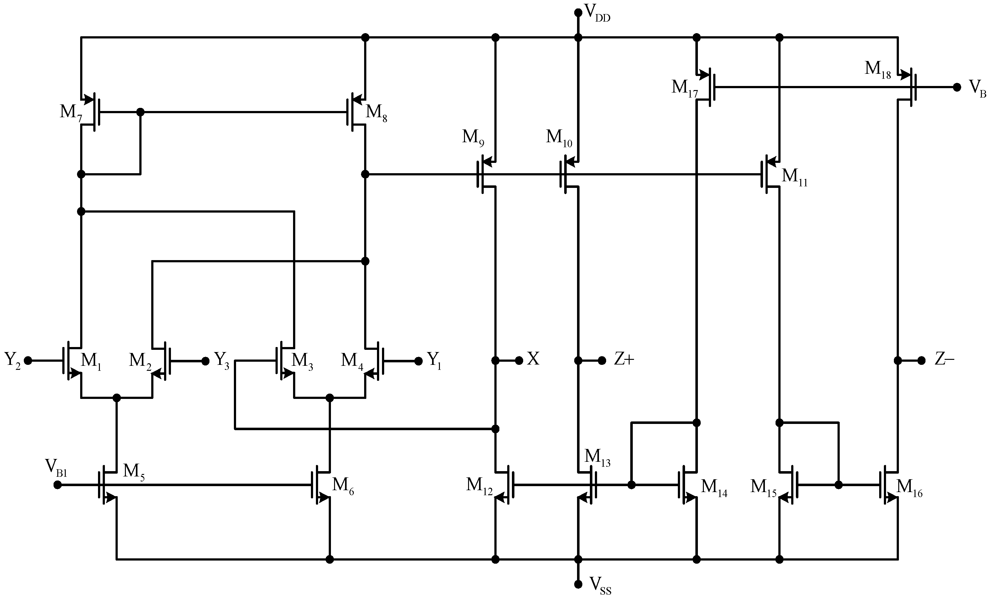
3.3. Non-Ideal Effect of Active Elements

Taking into account the non-idealities of DDCCs, the relationship of the terminal voltages and currents is given as
[ V X I Y 1 I Y 2 I Y 3 I Z ] = [ α k 1 α k 2 α k 3 0 0 0 0 0 0 0 0 0 0 0 0 0 0 0 0 ± β k ] [ V Y 1 V Y 2 V Y 3 I X ]
where αk1, αk2 and αk3 respectively denote the voltage tracking errors from VY1 to VX, VY2 to VX, and VY3 to VX of the kth DDCC; and βk denotes the current tracking error of the kth DDCC. The denominator of non-ideal transfer function of all obtained filters can be expressed by (39).
D ( s ) = α 1 i β 1 s 2 C 1 C 2 + s C 2 G 1 + α 2 j α 3 k β 2 β 3 G 2 G 3
where i, j, k = 1–2. The pole frequency ω0 and the Q factor are expressed by (40) and (41), respectively. The active and passive sensitivities of ω0 and Q of all obtained filters are shown in (42). It can be seen that all active and passive sensitivities are small.
ω 0 = α 2 j α 3 k β 2 β 3 G 2 G 3 α 1 i β 1 C 1 C 2
Q = 1 G 1 α 1 i α 2 j α 3 k β 1 β 2 β 3 C 1 G 2 G 3 C 2
S G 2 , G 3 ω 0 = S C 1 , C 2 ω 0 = S C 1 , G 2 , G 3 Q = S C 2 Q = 1 2 ; S G 1 Q = 1 ; S β 2 , β 3 ω 0 = S β 1 , β 2 , β 3 Q = 1 2 ; S β 1 ω 0 = 1 2 ; S α 2 j , α 3 k ω 0 = S α 1 i , α 2 j , α 3 k Q = 1 2 ; S α 1 i ω 0 = 1 2 ;

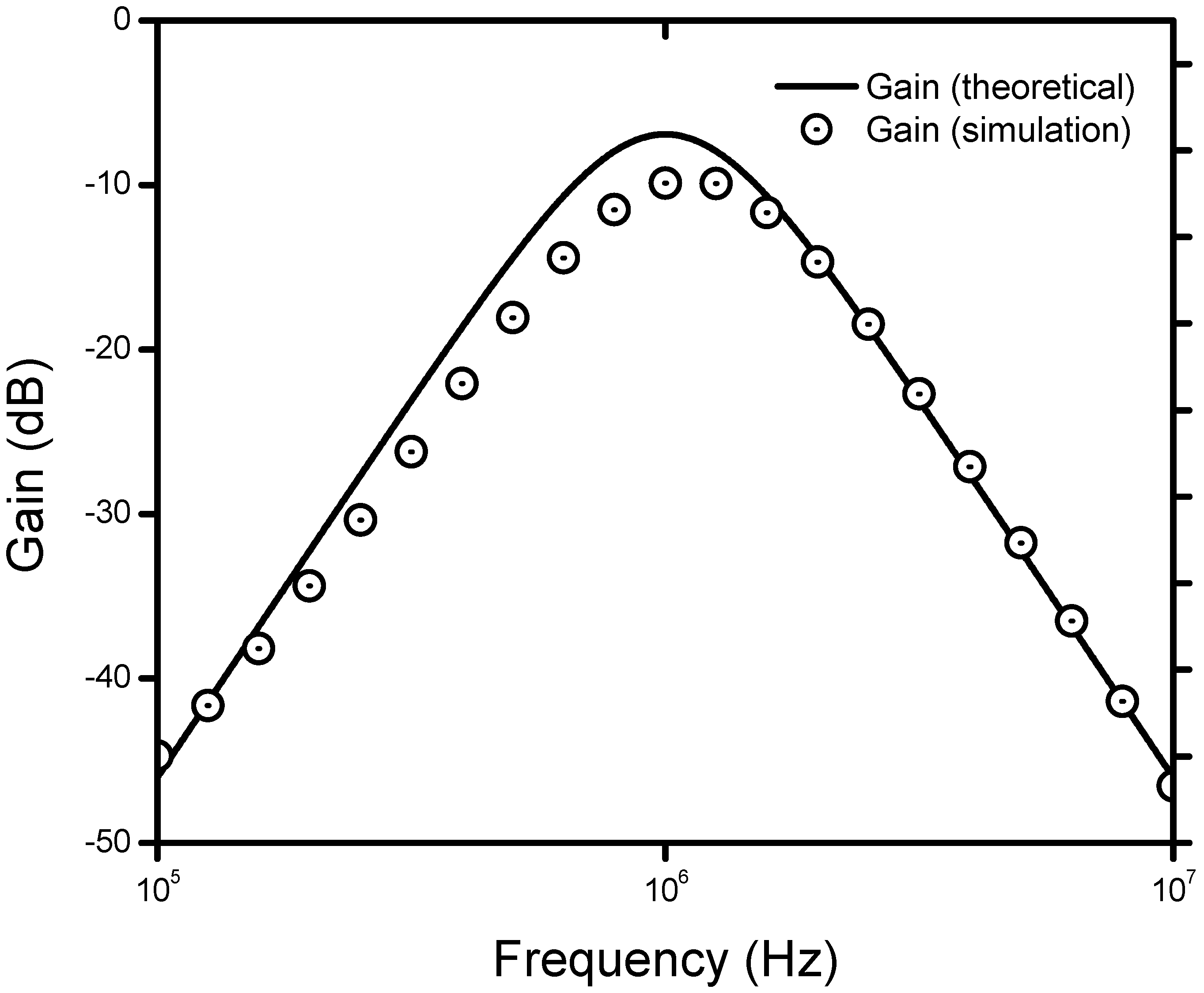
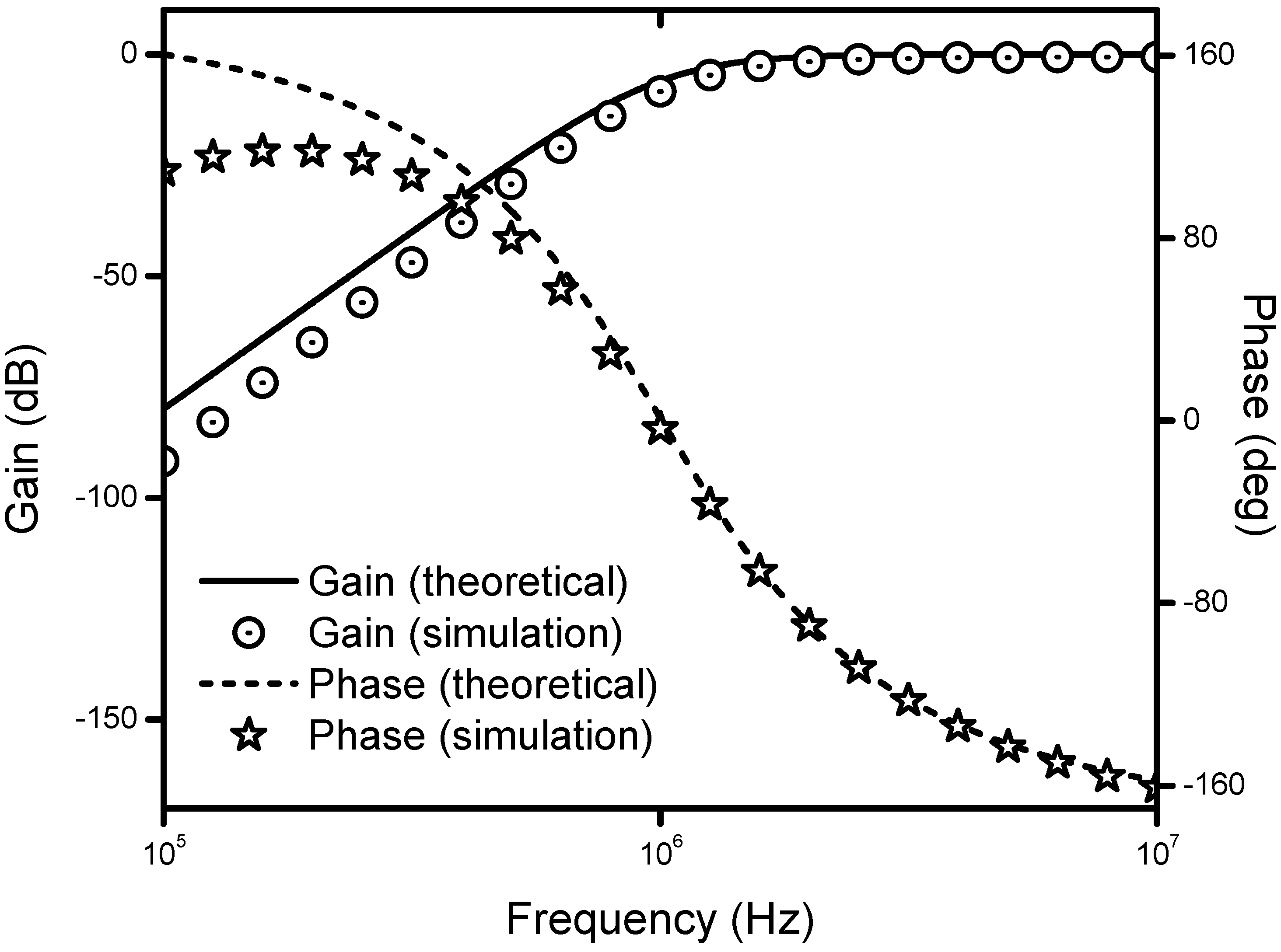
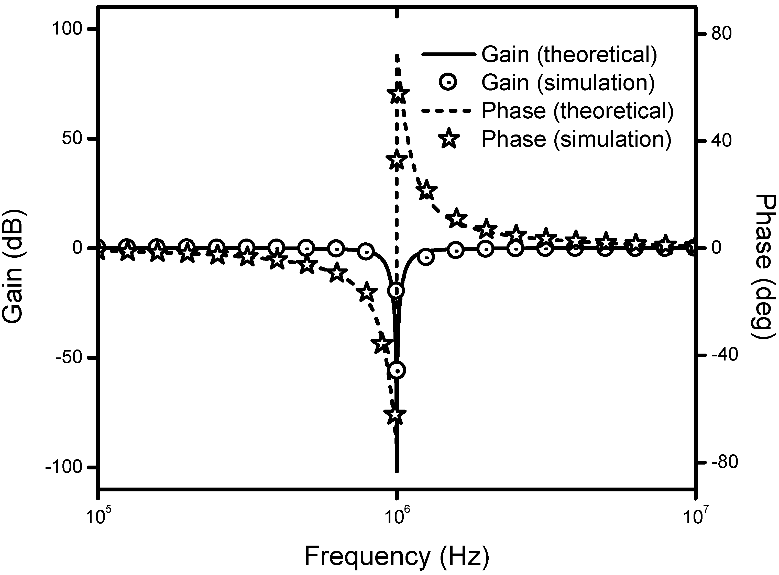
4. Simulation Results
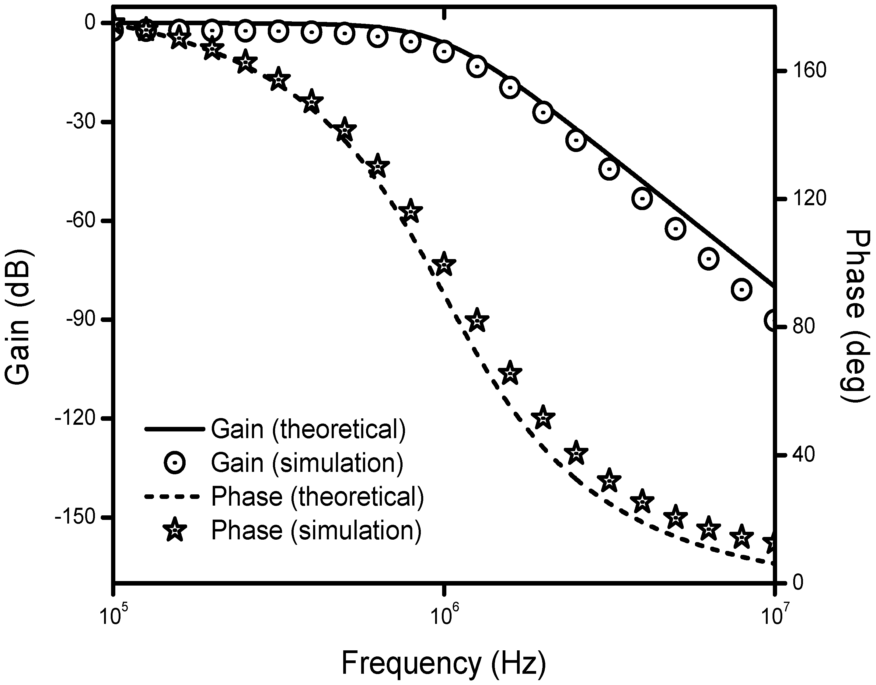
To verify the workability of the proposed method, HSPICE simulations using TSMC 0.35 μm process parameters were performed for two of the obtained type-A and type-B filters. The CMOS implementation of the DDCC shown in Figure 8 was used for the simulations [27]. The aspect ratios of each NMOS and PMOS transistor are (W/L = 5 μm/1 μm) and (W/L = 10 μm/1 μm), respectively. The supply voltages of DDCC are VDD = −VSS = 1.65 V with the biasing voltages VB = −VB1 = 0.76 V.
We simulated the filters in Figure 5f (type-A) and Figure 7b (type-B) for illustration. The values of capacitors are chosen as C1 = C2 = 10 pF for all simulations. The values of resistors are given by R1 = 11.26 kΩ and R2 = R3 = 15.92 kΩ for the simulations of lowpass, bandpass and highpass filters. Figure 9 and Figure 10 show the lowpass and bandpass responses at Vout1 and Vout2 of the filter in Figure 5f with node Vin3 as input node and nodes Vin1, Vin2, and Vin4 being ground node. The frequency responses of highpass output in Figure 5f with node Vin1 as input node and nodes Vin2, Vin3, and Vin4 being grounded is shown in Figure 11. Figure 12 shows the notch responses at Vout1 of the circuit in Figure 7b, with the merged node of Vin1 and Vin5 as input node and nodes Vin2, Vin3 and Vin4 being ground node, and R1 = 79.62 kΩ, R2 = R2 = R3 = 15.92 kΩ. Figure 13 represents the frequency responses of the allpass function in Figure 7b with the merged node of Vin1, Vin4, and Vin5 as input node and Vin2 and Vin3 grounded. The R1 = R2 = 11.26 kΩ and R3 = 22.52 kΩ is used. All the simulated results are consistent with our theoretical prediction. The workability of the synthesized filters is verified.
Figure 8. The CMOS circuit of DDCC [27].
Applsci 05 00320 g008
Figure 9. Frequency responses of the lowpass function in Figure 5f.
Applsci 05 00320 g009
Figure 10. Frequency responses of the bandpass function in Figure 5f.
Applsci 05 00320 g010
Figure 11. Frequency responses of the highpass function in Figure 5f.
Applsci 05 00320 g011
Figure 12. Frequency responses of the notch function in Figure 7b.
Applsci 05 00320 g012
Figure 13. Frequency responses of the allpass function in Figure 7b.
Applsci 05 00320 g013

5. Conclusions

Based on the infinity-variables notation of the DDCC and NAM expansion technique, a systematic method for synthesis of voltage-mode DDCC-based universal biquadratic filters is proposed. The obtained filters with two outputs can realize all five generic filter functions. They have the properties of high-input impedance, employing only grounded capacitors and resistors, orthogonal controllability between pole frequency and quality factor, and low active and passive sensitivities. HSPICE simulated results show the workability of the synthesized circuits, and the feasibility of the proposed approach is confirmed.

Acknowledgments

This work has been supported by the Ministry of Science and Technology of the Republic of China (Grant No. MOST 103-2221-E-151-060).

Author Contributions

Huu-Duy Tran and Quoc-Minh Nguyen conceived and designed the theoretical verifications; the optimization ideas were provided by Min-Chuan Lin; Hung-Yu Wang and Huu-Duy Tran analyzed the results and wrote the paper.

Conflicts of Interest

The authors declare no conflict of interest.

References

  1. Fabre, F.; Dayoub, L.; Duruisseau, L.; Kamoun, M. High-input impedance insensitive second-order filters implemented from current conveyors. IEEE Trans. Circuits Syst. I 1994, 41, 918–921. [Google Scholar]
  2. Chen, H.P. Single CCII-based voltage-mode universal filter. Analog Integr. Circuits Signal Process. 2010, 62, 259–262. [Google Scholar]
  3. Horng, J.W. High-input impedance voltage-mode universal biquadratic filters with three inputs using plus-type CCIIs. Int. J. Electron. 2004, 91, 465–475. [Google Scholar]
  4. Chen, H.P. Single FDCCII-based universal voltage-mode filter. AEU-Int. J. Electron. Commun. 2009, 63, 713–719. [Google Scholar]
  5. Horng, J.W. High-input impedance voltage-mode universal biquadratic filters using three plus-type CCIIs. IEEE Trans. Circuits Syst. II 2001, 48, 996–997. [Google Scholar]
  6. Chen, H.P. Voltage-mode FDCCII-based universal filter. AEU-Int. J. Electron. Commun. 2008, 62, 320–323. [Google Scholar]
  7. Horng, J.W.; Hou, C.L.; Chang, C.M.; Chou, H.P.; Lin, C.T. High-input impedance voltage-mode universal biquadratic filter with one input and five outputs using current conveyors. Circuits Syst. Signal Process. 2006, 25, 767–777. [Google Scholar] [CrossRef]
  8. Horng, J.W.; Hou, C.L.; Chang, C.M.; Chung, W.Y.; Wei, H.Y. Voltage-mode universal biquadratic filters with one input five outputs using MOCCIIs. Comput. Electr. Eng. 2005, 31, 190–202. [Google Scholar] [CrossRef]
  9. Chang, C.M.; Tu, S.H. Universal voltage mode filter with four inputs and one output using two CCII+s. Int. J. Electron. 1999, 86, 305–309. [Google Scholar] [CrossRef]
  10. Chang, C.M. Multifunction biquadratic filters using current conveyors. IEEE Trans. Circuits Syst. II 1997, 44, 956–958. [Google Scholar] [CrossRef]
  11. Haigh, D.G.; Clarke, T.J.W.; Radmore, P.M. Symbolic framework for linear active circuits based on port equivalence using limit variables. IEEE Trans. Circuits Syst. I 2006, 53, 2011–2024. [Google Scholar] [CrossRef] [Green Version]
  12. Haigh, D.G. A method of transformation from symbolic transfer function to active-RC circuit by admittance matrix expansion. IEEE Trans. Circuits Syst. I 2006, 53, 2715–2728. [Google Scholar] [CrossRef]
  13. Haigh, D.G.; Tan, F.Q.; Papavassiliou, C. Systematic synthesis of active-RC circuit building-blocks. Analog Integr. Circuits Signal Process. 2005, 43, 297–315. [Google Scholar] [CrossRef]
  14. Haigh, D.G.; Radmore, P.M. Admittance matrix models for the nullor using limit variables and their application to circuit design. IEEE Trans. Circuits Syst. I 2006, 53, 2214–2223. [Google Scholar] [CrossRef]
  15. Saad, R.A.; Soliman, A.M. Use of mirror elements in the active device synthesis by admittance matrix expansion. IEEE Trans. Circuits Syst. I 2008, 55, 2726–2735. [Google Scholar] [CrossRef]
  16. Soliman, A.M. Generation of current mode filters using NAM expansion. Int. J. Circuit Theory Appl. 2011, 39, 1087–1103. [Google Scholar] [CrossRef]
  17. Tan, L.; Bai, Y.; Teng, J.; Liu, K.; Meng, W. Trans-impedance filter synthesis based on nodal admittance matrix expansion. Circuits Syst. Signal Process. 2013, 32, 1467–1476. [Google Scholar] [CrossRef]
  18. Li, Y.A. NAM expansion method for systematic synthesis of floating gyrators using CCCCTAs. Analog Integr. Circuits Signal Process. 2015, 82, 733–743. [Google Scholar] [CrossRef]
  19. Tran, H.D.; Wang, H.Y.; Nguyen, Q.M.; Chiang, N.H.; Lin, W.C.; Lee, T.F. High-Q biquadratic notch filter synthesis using nodal admittance matrix expansion. AEU-Int. J. Electron. Commun. 2015, 69, 981–987. [Google Scholar] [CrossRef]
  20. Li, Y.A. On the systematic synthesis of OTA-based Wien Oscillators. AEU-Int. J. Electron. Commun. 2013, 67, 754–760. [Google Scholar] [CrossRef]
  21. Soliman, A.M. Two integrator loop filters: Generation using NAM expansion and review. J. Electri. Comput. Eng. 2010. [CrossRef]
  22. Chiu, W.; Liu, S.I.; Tsao, H.W.; Chen, J.J. CMOS differential difference current conveyors and their applications. IEE Proc. Circuits Devices Syst. 1996, 143, 91–96. [Google Scholar] [CrossRef]
  23. Chiu, W.Y.; Horng, J.W. High-input and low-output impedance voltage-mode universal biquadratic filter using DDCCs. IEEE Trans. Circuits Syst. II 2007, 54, 649–652. [Google Scholar] [CrossRef]
  24. Chen, H.P. Universal voltage-mode filter using only plus-type DDCCs. Analog Integr. Circuits Signal Process. 2007, 50, 137–139. [Google Scholar] [CrossRef]
  25. Horng, J.W. High input impedance voltage-mode universal biquadratic filter with three inputs using DDCCs. Circuits Syst. Signal Process. 2008, 27, 553–562. [Google Scholar] [CrossRef]
  26. Chiu, W.Y.; Horng, J.W. High input impedance voltage-mode biquadratic filter with three inputs and six outputs using three DDCCs. Circuits Syst. Signal Process. 2012, 31, 19–30. [Google Scholar] [CrossRef]
  27. Elwan, H.O.; Soliman, A.M. Novel CMOS differential voltage current conveyor and its applications. IEE Proc. Circuits Devices Syst. 1997, 144, 195–200. [Google Scholar] [CrossRef]

