Article

A Micro-Processor-Based Feedback Stabilization Scheme for High-Q, Non-Linear Silicon Resonators

by
Giuseppe Cantarella
and
Michael J. Strain
*
Institute of Photonics, Department of Physics, University of Strathclyde, Glasgow G1 1RD, UK
*
Author to whom correspondence should be addressed.
Appl. Sci. 2016, 6(11), 316; https://doi.org/10.3390/app6110316
Submission received: 11 October 2016 / Revised: 20 October 2016 / Accepted: 21 October 2016 / Published: 25 October 2016
(This article belongs to the Special Issue Silicon Photonics Components and Applications)

Abstract

:
Stabilization of silicon micro-resonators is a key requirement for their inclusion in larger photonic integrated circuits. In particular, thermal refractive index shift in non-linear applications can detune devices from their optimal working point. A cavity stabilization scheme using a micro-processor-based feedback control loop is presented based on a local thermal heater element on-chip. Using this method, a silicon π -phase shifted grating with a cavity Q-factor of 40k is demonstrated to operate over an ambient temperature detuning range of 40 C and injection wavelength range of 1.5 nm, nearly 3 orders of magnitude greater than the resonant cavity linewidth.

1. Introduction

Due to strong optical mode confinement and significant non-linearities, silicon photonics is an attractive platform for non-linear optics [1]. A wealth of useful non-linear modes of operation have been demonstrated on this platform, including: Kerr non-linearity for Four-wave mixing (FWM) [2,3,4], super-continuum generation [5] and photon pair generation [6]; and thermal refractive index non-linearity for optical bistability and all-optical signal processing functions [7]. Enhancement of the non-linear effects in waveguide devices has been achieved through both material [8] and device design. In many cases, micro-resonator devices are used to enhance the non-linear interaction for low power, compact device designs [3,9,10,11,12]. The increased photon lifetime in the cavity and resonant enhancement of the field in a small mode volume allows for improved light-matter interaction, but additionally increases detuning effects on the resonator due to thermal refractive index variation of the resonant wavelength. In non-linear applications it is desirable to operate the system at the point of maximum resonant enhancement, which in turn requires the alignment of the resonator wavelength and input laser signal.
Typically, resonator-laser alignment is achieved at a given injection power by tuning the laser from the blue spectral side of the resonant line into the cavity. Gradually, the laser wavelength is increased, increasing the power in the cavity and therefore the thermally induced refractive index of the resonant line shift. The thermal refractive index increase shifts the resonant line to longer wavelengths as the laser wavelength approaches the cold cavity peak. Finally, at some detuning to the red side of the cold cavity peak, the thermally-induced refractive index shift is no longer sufficient to align the cavity resonance with the laser line and the system reverts to the cold cavity state. Figure 1 shows a typical measured transmission spectrum for a silicon waveguide resonator where the injected power is sufficient to induce a thermal refractive index effects. The device is a π -phase shifted Bragg grating, the details of which will be discussed in Section 2.1.
In addition to the thermal refractive index detuning induced by optical absorption, devices are also subject to variations in the environmental conditions, with silicon exhibiting a relatively high thermal coefficient of refractive index, 1.8 × 10 4 K 1 [13]. For example, the resonant wavelength of a Bragg grating device is given by λ B = 2 n e f f Λ 0 , where n e f f is the modal effective index and Λ 0 is the grating period. So a change of 0.1 K on a grating with a period of 318 nm and an effective index of 2.445 , can result in a resonance shift of over 10 pm. This is on the order of the linewidth of a high-Q cavity resonance, and therefore can significantly affect the operation of the device given a fixed wavelength laser injection, essentially detuning the device resonant wavelength from the laser signal. Furthermore, a shift of the laser wavelength to the red with respect to the cavity working point can essentially ‘switch off’ the non-linear device operation as the resonant enhancement reverts to the cold cavity case. This produces discontinuities in any experimental setup using the device in this mode and is to be avoided. In a temperature controlled laboratory setting with devices mounted on Peltier control stages device stability is often only in the order of minutes due to the picometre tuning range that is tolerable between the laser wavelength and cavity wavelength.
There have been a number of demonstrations of cavity stabilization in silicon photonic devices using both electrical [14] and thermal [15] elements on-chip. These schemes have been primarily designed for tracking of the cavity line in linear optical applications such as data communications. Since the cavity lineshape is symmetric in these regimes, active control schemes using dithering are suitable. However, in the case of non-linear applications, the signal wavelength cannot be dithered since this will push the device past the ‘switch-off’ point on the long wavelength side.
In this work a means is presented by which cavities operating in the non-linear regime can be actively stabilized using a simple thermal control element. In Section 2 the device technology and fabrication processes are presented along with experimental setup designs and details of the stabilization scheme. Section 3 details the results of linear and non-linear optical measurements under direct stabilization control.

2. Materials and Methods
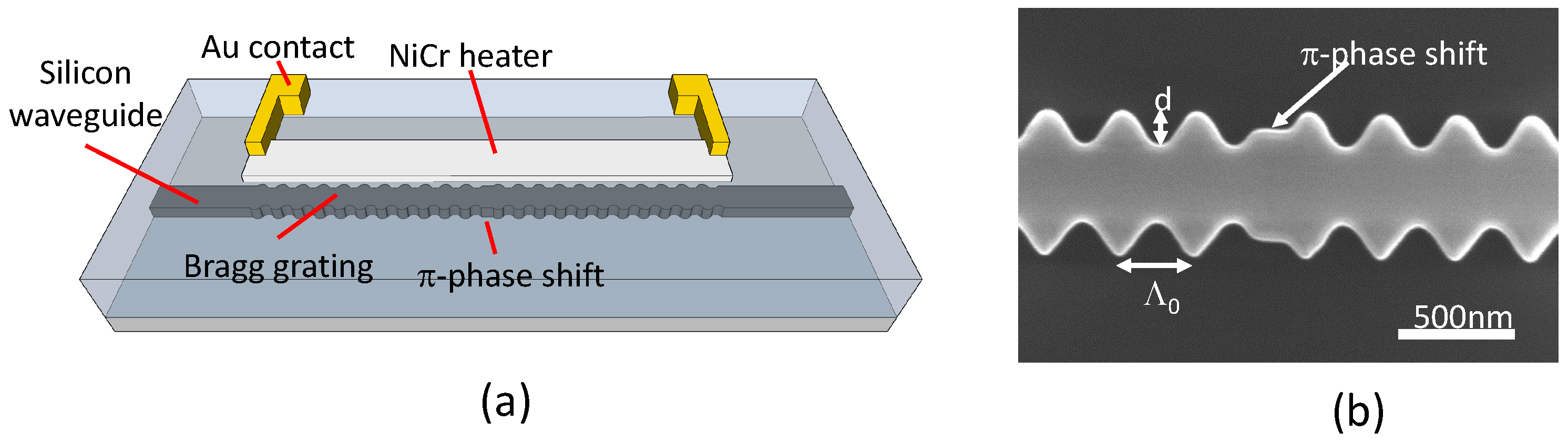
2.1. π -Phase Shifted Bragg Grating Design and Fabrication

To demonstrate the effects of active stabilization on high-Q cavity resonators this work takes a π -phase shifted Bragg grating geometry as an example, though the effects are generally applicable across resonator types. π -phase shifted gratings have demonstrated high-Q factors [16], whilst maintaining moderate cavity lengths and single resonance line operation. The grating presented here is realized as a sidewall modulation of the silicon ridge waveguide [17]. This scheme allows simple integration with single mode waveguides with direct control over the grating spectral characteristics through modulation of the grating period and modulation amplitude [18]. The π -phase shift is fabricated as a half period delay in the grating modulation at the centre of the device. This is easily created as a section of straight waveguide. The grating delay of Λ 0 / 2 is realized at the midpoint of the perturbation amplitude in order to create a π -phase shift with a geometric length of half a grating period. Placing the delay at either the peak or trough of the perturbation would create a different effective modal index and therefore modify the phase delay. A schematic of the device is shown in Figure 2a, with a scanning electron microscope (SEM) image of the π -phase shift section in Figure 2b.
The cavity wavelength tuning mechanism used in this work is achieved by fabricating a thermal tuning element above the grating device, as shown in Figure 2a. By applying a voltage across the heater element, localized temperature variations can be applied to the device and therefore control exerted over its resonance wavelength [11,14]. The devices fabricated in this work were produced on a SOI wafer (SOITEC, Bernin, France) with a 220 nm thick silicon core. Gratings were defined using e-beam lithography with Hydrogen Silsequioxane as a mask. The waveguides were nominally 500 nm wide with a 5 nm perturbation amplitude, d. The grating was 628.5 periods long. The devices were clad with a Plasma Enhanced Chemical Vapour Deposition (PECVD) silica layer and a spin-on-glass coating (DOW corning, Midland, MI, USA), and finally a resistive heater was fabricated directly above the grating as an 800 nm wide, 50 nm thick layer of NiCr. The NiCr heater was contacted using low resistance gold tracks.

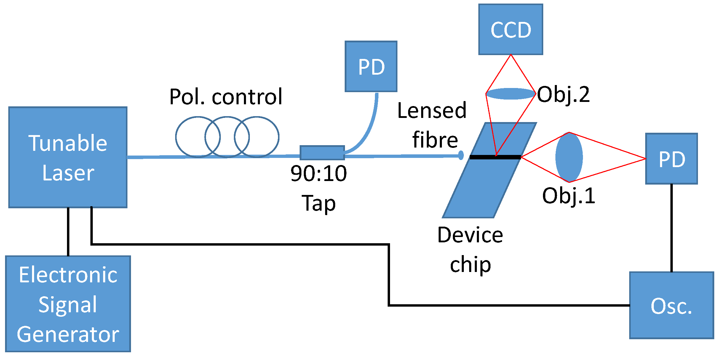
2.2. Optical Transmission Measurement Setup

All of the measurements presented in this work were carried out using an end-fire setup as shown in Figure 3. Light from a tunable laser, Agilent 81640A (Keysight Technologies Deutschland GmbH, Böblingen, Germany), was coupled onto the silicon chip via polarization control optics and a lensed optical fibre. The top scattering from the chip was measured using a compact InGaAs camera (Xenics nv, Leuven, Belgium), and the output facet was imaged onto a photo-detector via a microscope objective (Comer optics, Linton, UK). Transmission spectra were measured by using the tunable laser in swept mode and measuring the time dependent detected power on the oscilloscope (Keysight Technologies Deutschland GmbH, Böblingen, Germany).

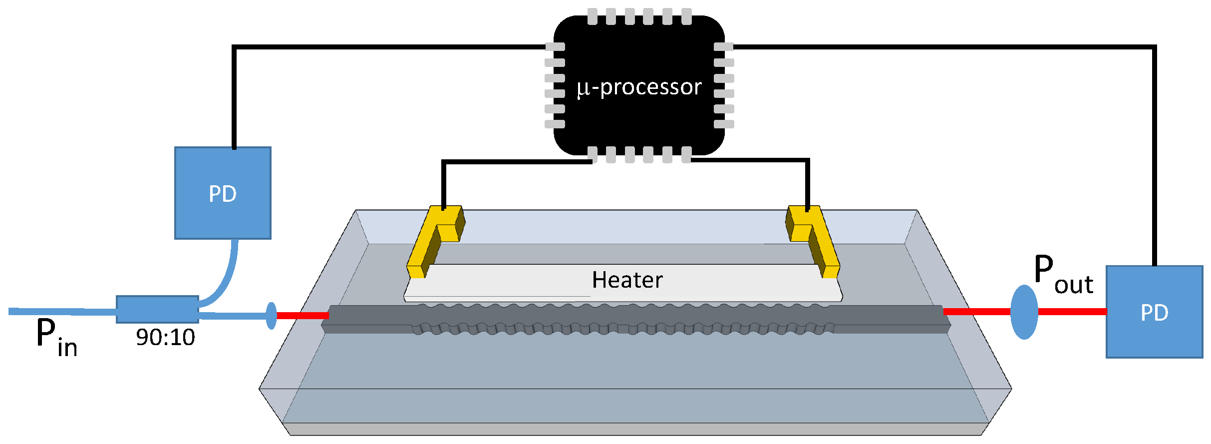
2.3. Cavity Stabilization Scheme

The relative position of the laser injection wavelength and cavity resonance can be controlled using the local thermal heater detailed above. This scheme makes the device robust to changes in either the laser wavelength or global thermal shifts of the cavity resonance position. In order to avoid dithering of the cavity resonance that will push the device out of the resonant operation window, this method makes use of the known spectral transfer function of the device. By measuring the cold cavity spectrum, the linear losses, resonator Q-factor and lineshape, and central resonant wavelength can be measured. Given the thermal refractive index coefficient of silicon, along with the absorption in the resonator and thermal dissipation, the transfer function can be calculated as a function of injection power [7]. Figure 4 shows simulated transmission spectra of a π -phase shifted grating with the parameters matching the fabricated device with injection power as parameter. The simulation was carried out using a transfer matrix method (TMM) solution to the coupled mode equations [19], where the refractive index is a function of the power in the resonator mode volume. In this work injection power refers to the optical power in the access waveguide coupled to the resonator, and transmission refers to the power in the post-resonator waveguide. The characteristic asymmetric resonance shape is visible with injection powers as low as 0.09 mW.
A schematic of the stabilization arrangement is presented in Figure 5. Given the transfer function of the resonator and a measurement of the input power, the resonator response can be easily calculated using the simple TMM model, which can be stored in a microprocessor controller. To stabilize the device the user sets the device manually to the optimal working point then initiates the feedback control system. If the relative position of the resonator and laser injection wavelength changes this will create an error signal dependent on the shift away from the calculated operating point and the spectral model. This error signal can then be fed-back to the local thermal heating element to shift the position of the resonant line. Any injection power changes are captured by the power tap at the input of the system.

3. Results and Discussion
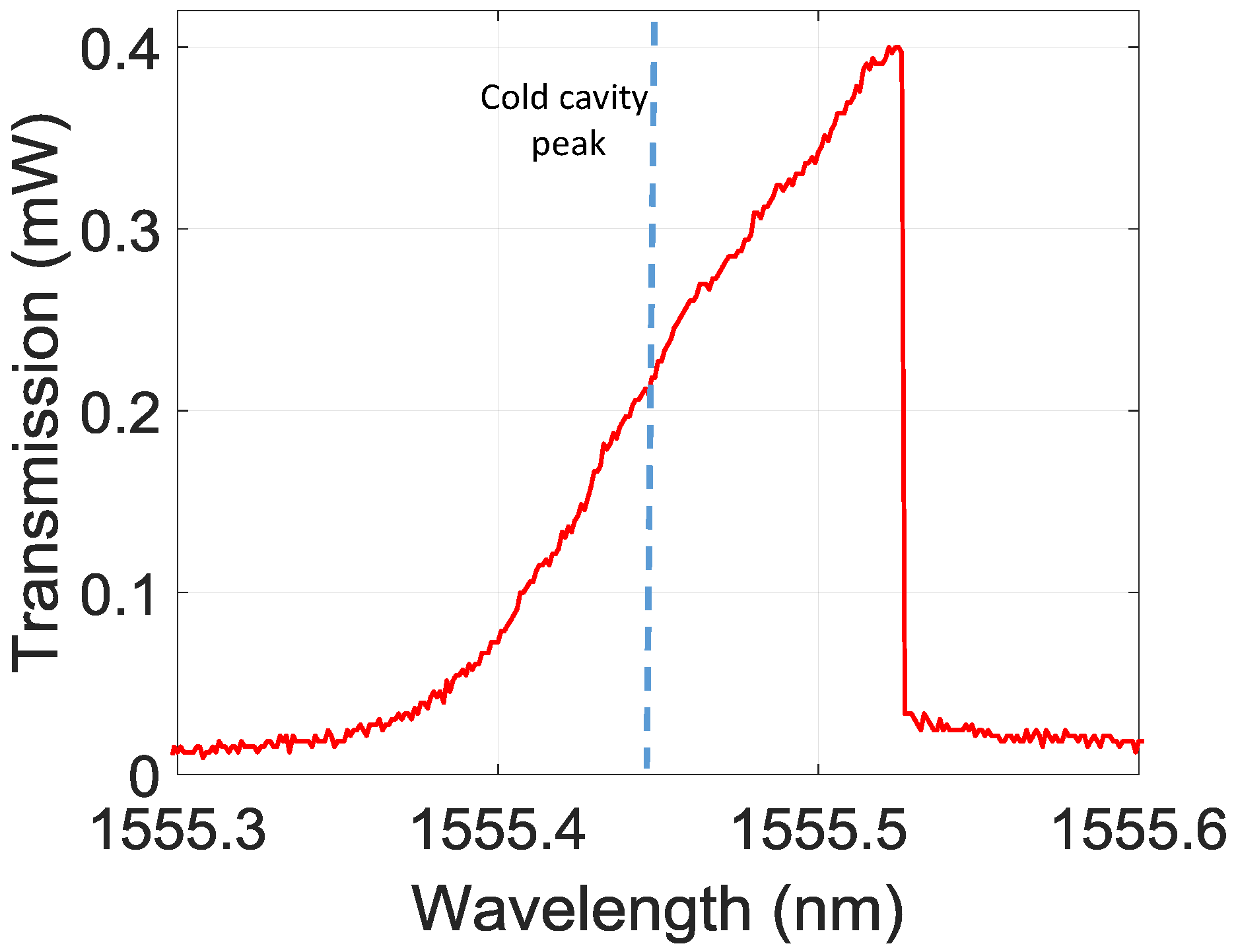
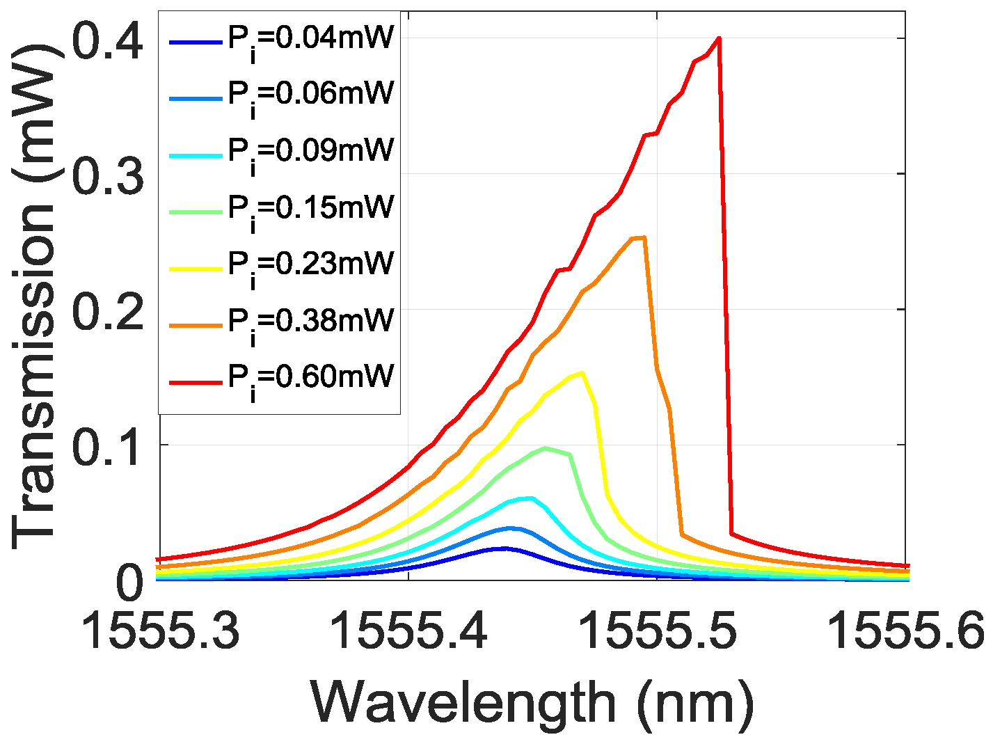
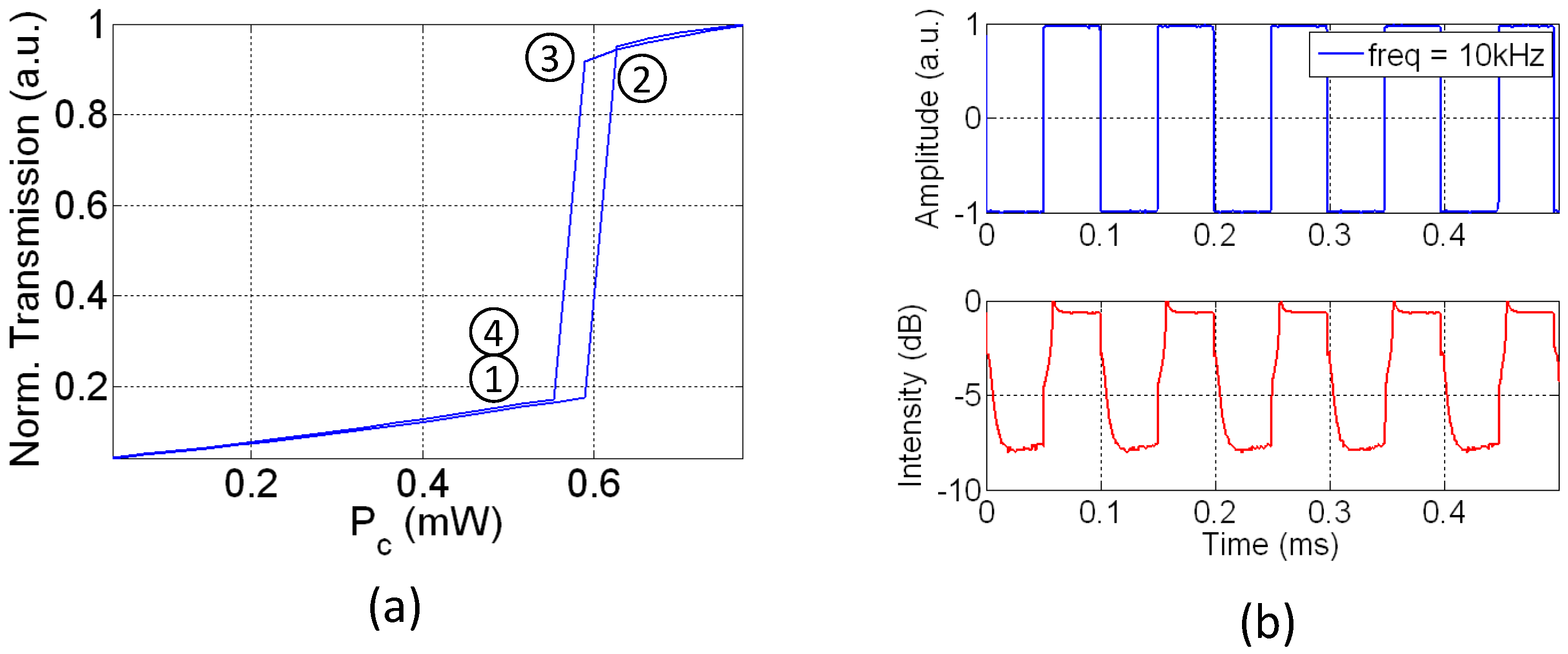
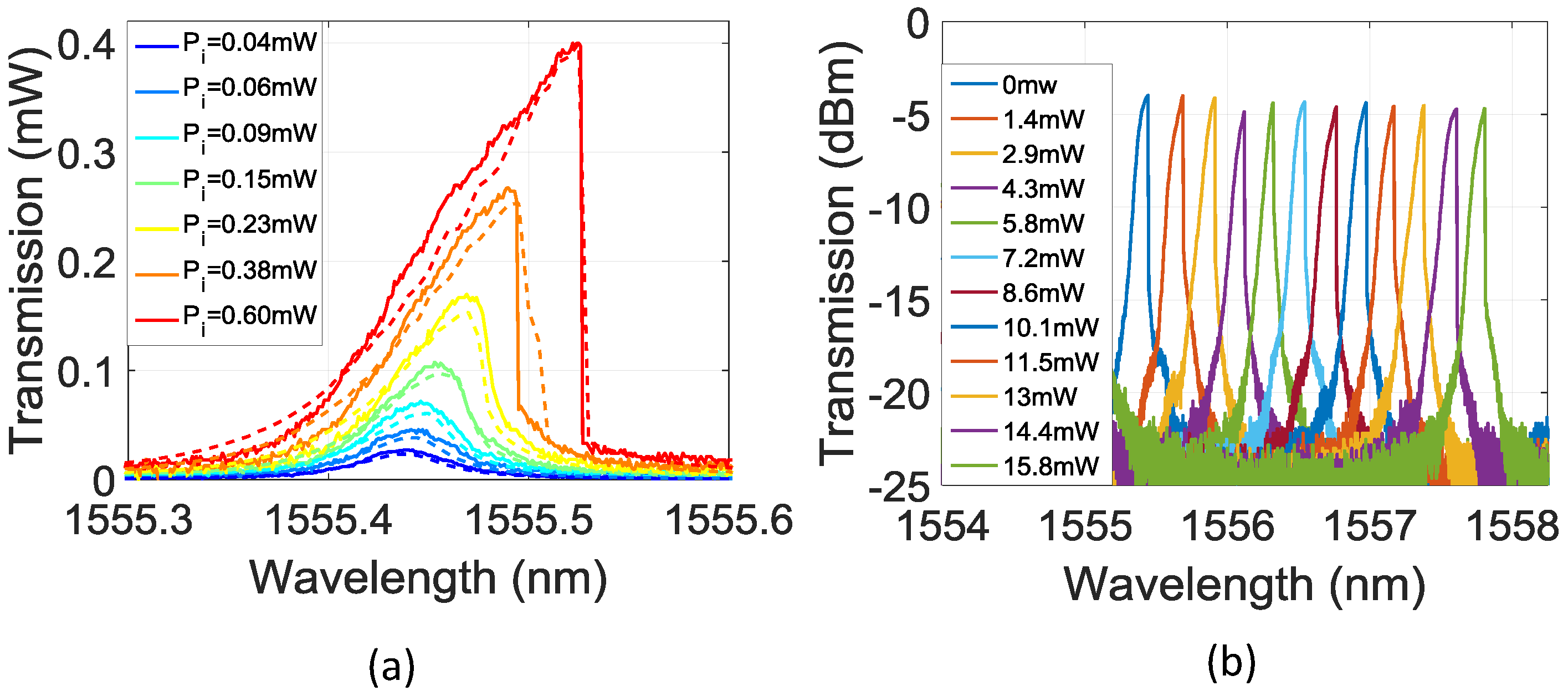
3.1. π -Phase Shifted Grating Response

Figure 6a shows the measured transmission spectrum of the π -phase shifted grating device, with a low injection power to avoid non-linear effects. The inset shows an enlargement of the resonance mode, with a Q-factor of ≈40 k. Figure 6b shows near-infrared (NIR) camera images of the light scattered vertically from the grating filter and access waveguides, where light is injected from the left hand side of the images. These images were taken before fabrication of the metal heater elements. (I) is the out of band transmission, showing scattering along the waveguide length; (II) is the in-band rejection showing little light transmitted from the input to the output waveguide; and (III) is the on-resonance transmission mode showing clear localization to the centre of the grating device.
Figure 7a presents the measured transmission spectra of the device as a function of input power, along with the simulated spectra from Figure 4. The onset of the thermal non-linear behaviour is clear at around 0.09 mW of power on-chip. Figure 7b shows the tuning effect of the on-chip thermal heating element. By increasing the the power dissipated on the heater the global spectrum of the device can be shifted to longer wavelengths, whilst still retaining the non-linear thermal resonance shift as a function of injected optical power.
For the stabilization experiments, the device is operated at its maximum resonance position for an injection power of 0.6 mW. In order to demonstrate that the device remains in this optimal condition, a measure of the resonant enhancement is required. Here, the bistable switching of the cavity [7], was chosen as a convenient demonstration. Figure 8a shows the measured hysteresis curve for the resonator with an injection wavelength set at the optimal working point. At point (1) the laser wavelength is on the red side of the resonance line and at a low value of transmission. Increasing the injection power to point (2) increases the power trapped in the resonator, red-shifting the resonance line towards the injection wavelength setting the device to the high transmission state. The trapped optical power maintains this high transmission state as a function of reducing power through point (3). At this point the power is insufficient to cause a red shift alignment of the resonant line with the injection wavelength and the resonator returns to point (4) where its cavity resonance line is blue detuned from the laser wavelength and the device is in the low transmission state.
The temporal bistable switching operation used to monitor the device operation was achieved by using a signal generator to apply a direct modulation to the tunable laser output power. The laser was set at an average power on-chip of 0.6 mW with a modulation amplitude of 0.09 mW. In addition, to allow positive and negative detuning via the thermal heating element, the device is operated with an initial bias on the heater. All the results below were taken at an initial operating wavelength of 1556.980 nm. A square wave at 10 kHz was used as a source, with the optical device temporal response shown in Figure 8b. The extinction of the switching depends on the working point of the device with respect to the cavity resonance. The maximum extinction in this case is 7.5 dB. The extinction ratio can then be taken as a measure of the operating point of the system. Figure 9 shows the measured bistable switching extinction ratio as a function of laser signal detuning from the optimal working point. (i) As the wavelength is tuned from the blue towards the cold cavity peak of the resonance the extinction increases. (ii) As the injection wavelength approaches the peak of the resonance, the device starts to exhibit incomplete bistable switching with an increasing portion of the duty cycle switched to the low state. (iii) Full switching is achieved with increasing extinction as the optimal working point is approached. (iv) Finally, the wavelength moves too far to the red side of the resonance peak to induce bistable switching and the device is in the low state. It is worth noting that the detuning range of the optimal bistable region (iii) is less than 7 pm in terms of injection laser wavelength detuning, illustrating the necessity for device stabilization.

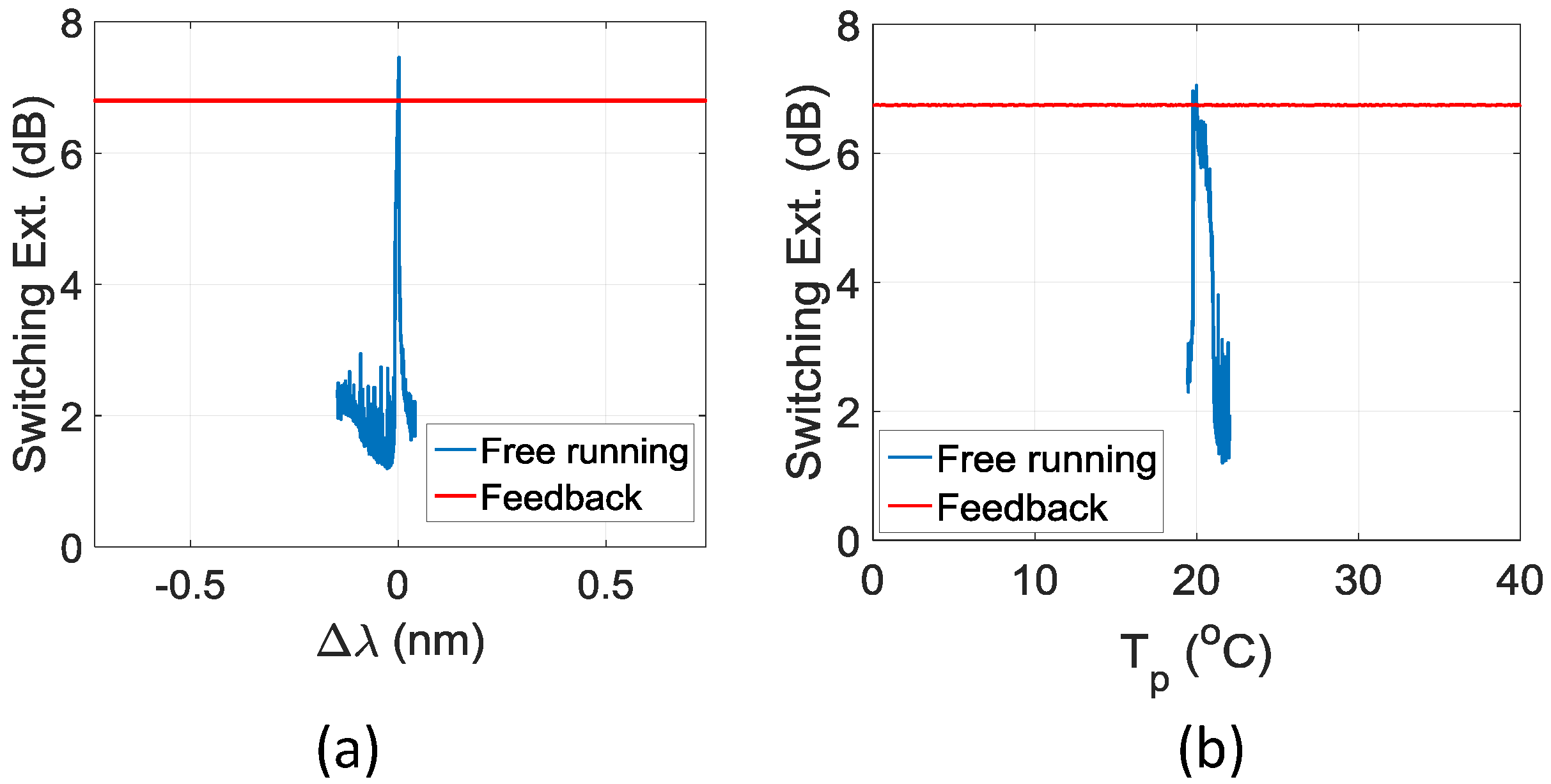
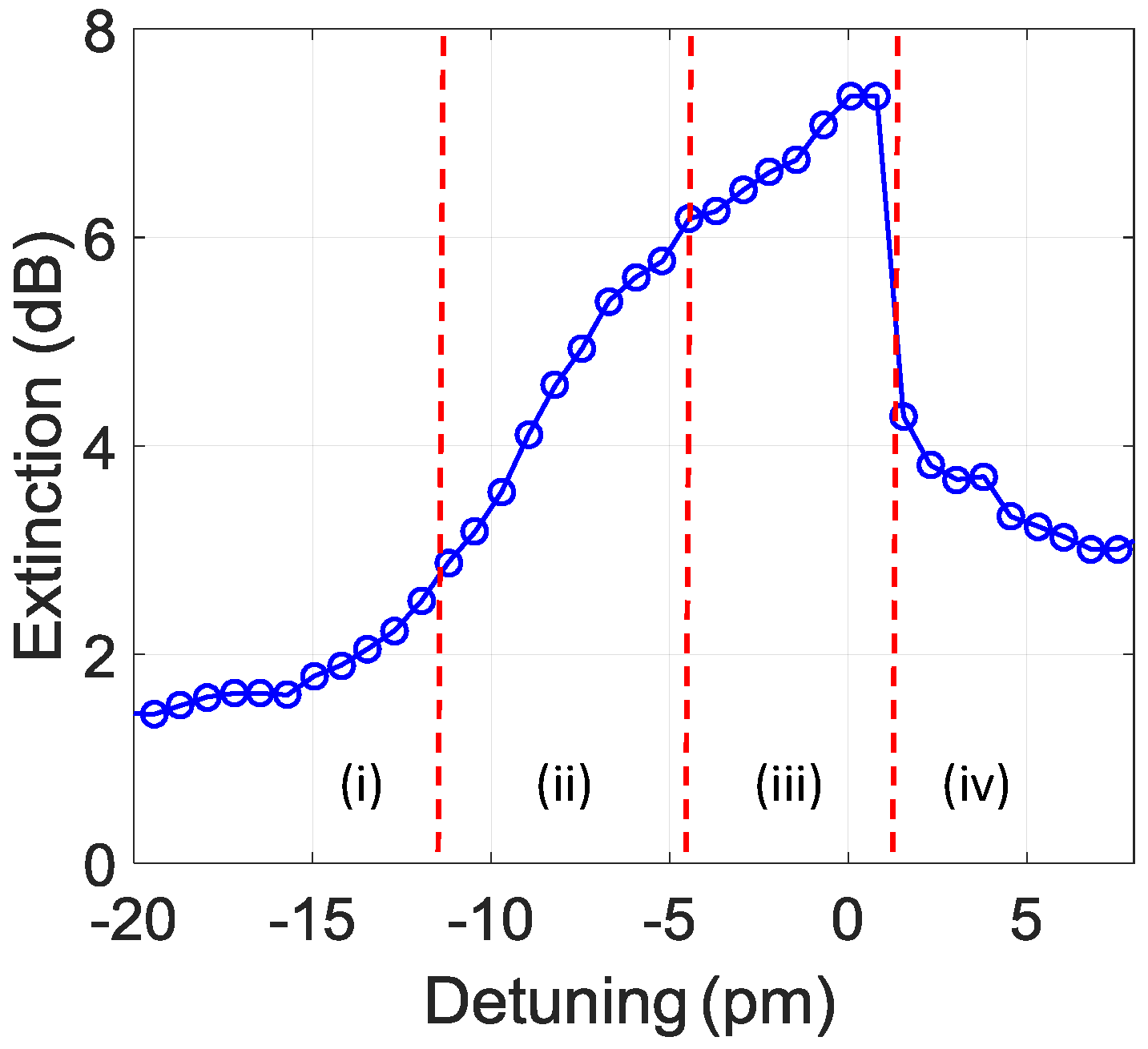
3.2. Cavity Stabilization

As mentioned previously, the device was mounted on a Peltier control stage in a thermally controlled laboratory environment. Nevertheless, in the free running case, after initializing the system at its optimal working point, the lifetime of operation was in the order of minutes. When the feedback system was enabled there was no observed drift in measured extinction ratio of the bistable switching over an 8 h period of operation. The system was then forced by detuning the laser injection wavelength from the optimal working point in both positive and negative directions from the set-point. Figure 10a shows the switching extinction ratio as a measure of operation in the bistable regime for laser detuning wavelength. Behaviour of the system is shown for both the free running case and where the feedback system has been engaged. For the case with no feedback control the bistable switching exists over only a few picometres of laser detuning as expected. When the control loop is engaged the laser wavelength can be detuned over a 1.5 nm range without affecting the bistable switching operation, limited only by the resistive heater’s operation range.
Finally, the Peltier stage was used to vary the ambient thermal conditions of the device. The temperature values detailed in Figure 10b relate to measurements on the surface of the Peltier stage in contact with the silicon substrate of the device. The lab was kept at a constant temperature of 20 C throughout the measurements. A temperature variation of only ≈1 C is sufficient to detune the device from the bistable regime in the free running case. By enabling the feedback control, the system exhibits stable switching over a temperature range of 40 C, limited by the Peltier tuning range.

4. Conclusions

Stabilization of a high-Q micro-resonator operating in the non-linear regime was presented. An example device consisting of a silicon π -phase shifted grating was fabricated incorporating a local resistive heater element for wavelength tuning of the resonance. Bistable switching of the device at sub-mW injection powers was demonstrated and a simple transmission function method using a microprocessor-based feedback loop was detailed. In free running conditions, detuning of a few picometres in injection wavelength or 1 C in ambient temperature moves the resonator out of the bistable switching regime. By implementing a micro-processor-based feedback loop the device operates stably over a laser detuning range of 1.5 nm and a temperature range of 40 C.

Acknowledgments

The authors wish to thank Marc Sorel and the staff of the James Watt Nanofabrication Centre at the University of Glasgow. This work was partially supported by the Royal Society (RG140227).

Author Contributions

M.J.S. conceived and designed the experiments; G.C. and M.J.S. performed the experiments, analyzed the data and composed the manuscript.

Conflicts of Interest

The authors declare no conflict of interest.

References

  1. Leuthold, J.; Koos, C.; Freude, W. Nonlinear silicon photonics. Nat. Photonics 2010, 4, 535–544. [Google Scholar] [CrossRef]
  2. Foster, M.A.; Turner, A.C.; Salem, R.; Lipson, M.; Gaeta, A.L. Broad-band continuous-wave parametric wavelength conversion in silicon nanowaveguides. Opt. Express 2007, 15, 12949–12958. [Google Scholar] [CrossRef] [PubMed]
  3. Ong, J.R.; Member, S.; Kumar, R. Efficient CW Four-Wave Mixing in Silicon-on-Insulator Micro-Rings With Active Carrier Removal. IEEE Photonics Technol. Lett. 2013, 25, 1699–1702. [Google Scholar] [CrossRef]
  4. Wu, C.; Lin, Y.; Su, S.; Huang, B.; Lin, G.-R. Degenerate Four-Wave Mixing in Si Quantum Dot doped Si-rich SiNx Channel Waveguide. J. Light. Technol. 2016, 34, 4111–4120. [Google Scholar] [CrossRef]
  5. Kuyken, B.; Liu, X.; Osgood, R.M.; Baets, R.; Roelkens, G.; Green, W.M.J. Mid-infrared to telecom-band supercontinuum generation in highly nonlinear silicon-on-insulator wire waveguides. Opt. Express 2011, 19, 20172–20181. [Google Scholar] [CrossRef] [PubMed]
  6. Grassani, D.; Azzini, S.; Liscidini, M.; Galli, M.; Strain, M.J.; Sorel, M.; Sipe, J.E.; Bajoni, D. Micrometer-scale integrated silicon source of time-energy entangled photons. Optica 2015, 2, 88–94. [Google Scholar] [CrossRef]
  7. Almeida, V.R.; Lipson, M. Optical bistability on a silicon chip. Opt. Lett. 2004, 29, 2387–2389. [Google Scholar] [CrossRef] [PubMed]
  8. Wu, C.-L.; Lin, Y.-H.; Cheng, C.-H.; Su, S.-P.; Huang, B.-J.; Chang, J.-H.; Wu, C.-I.; Lee, C.-K.; Lin, G.-R. Enriching Si quantum dots in a Si-rich SiNx matrix for strong χ(3) optical nonlinearity. J. Mater. Chem. C 2016, 4, 1405–1413. [Google Scholar] [CrossRef]
  9. Turner, A.C.; Foster, M.A.; Gaeta, A.L.; Lipson, M. Ultra-low power parametric frequency conversion in a silicon microring resonator. Opt. Express 2008, 16, 4881–4887. [Google Scholar] [CrossRef] [PubMed]
  10. Morichetti, F.; Canciamilla, A.; Ferrari, C.; Samarelli, A.; Sorel, M.; Melloni, A. Travelling-wave resonant four-wave mixing breaks the limits of cavity-enhanced all-optical wavelength conversion. Nat. Commun. 2011, 2, 296. [Google Scholar] [CrossRef] [PubMed] [Green Version]
  11. Strain, M.J.; Lacava, C.; Merrigi, L.; Cristiani, I.; Sorel, M. Tunable Q-factor silicon micro-ring resonators for ultra-low power parametric processes. Opt. Lett. 2014, 40, 4–7. [Google Scholar]
  12. Grieco, A.; Slutsky, B.; Tan, D.T.H.; Zamek, S.; Nezhad, M.P.; Fainman, Y. Optical Bistability in a Silicon Waveguide Distributed Bragg Reflector Fabry-Pérot Resonator. IEEE J. Light. Technol. 2012, 30, 2352–2355. [Google Scholar] [CrossRef]
  13. Komma, J.; Schwarz, C.; Hofmann, G.; Heinert, D.; Nawrodt, R. Thermo-optic coefficient of silicon at 1550 nm and cryogenic temperatures. Appl. Phys. Lett. 2012, 101, 4–8. [Google Scholar] [CrossRef]
  14. Padmaraju, K.; Logan, D.F.; Shiraishi, T.; Ackert, J.J.; Knights, A.P.; Bergman, K. Wavelength locking and thermally stabilizing microring resonators using dithering signals. J. Light. Technol. 2014, 32, 505–512. [Google Scholar] [CrossRef]
  15. Padmaraju, K.; Logan, D.F.; Zhu, X.; Ackert, J.J.; Knights, A.P.; Bergman, K. Integrated thermal stabilization of a microring modulator. Opt. Express 2013, 21, 14342–14350. [Google Scholar] [CrossRef] [PubMed]
  16. Wang, X.; Shi, W.; Grist, S.; Yun, H.; Jaeger, N.A.F.; Chrostowski, L. Narrow-band transmission filter using phase-shifted Bragg gratings in SOI waveguide. In Proceedings of the IEEE Photonics Conference, Arlington, VA, USA, 9–13 October 2011.
  17. Rutkowska, K.A.; Duchesne, D.; Strain, M.J.; Morandotti, R.; Sorel, M.; Azaña, J. Ultrafast all-optical temporal differentiators based on CMOS-compatible integrated-waveguide Bragg gratings. Opt. Express 2011, 19, 19514–19522. [Google Scholar] [CrossRef] [PubMed]
  18. Strain, M.J.; Thoms, S.; MacIntyre, D.S.; Sorel, M. Multi-wavelength filters in silicon using superposition sidewall Bragg grating devices. Opt. Lett. 2014, 39, 413–416. [Google Scholar] [CrossRef] [PubMed]
  19. Strain, M.J.; Sorel, M. Design and fabrication of integrated chirped Bragg gratings for on-chip dispersion control. IEEE J. Quantum Electron. 2010, 46, 774–782. [Google Scholar] [CrossRef]
Figure 1. Measured transmission spectrum of a silicon π -phase shifted grating demonstrating resonantly enhanced thermal refractive index detuning effects.
Applsci 06 00316 g001
Figure 2. (a) Schematic of a silicon π -phase shifted grating with resistive heating element for wavelength tuning and thermal stabilization; (b) Scanning Electron Microscope (SEM) image of the phase shift section at the centre of a grating device (a device with d = 70 nm is shown to best illustrate the grating modulation profile).
Applsci 06 00316 g002
Figure 3. Schematic of the measurement setup. Obj.1 and 2 are objective lenses for imaging the device facet and top surface respectively, PD are photodiodes and Osc. is a digital oscilloscope. CCD is an InGaAs CCD camera.
Applsci 06 00316 g003
Figure 4. Simulated transmission spectra of a π -phase shifted grating as a function of injection power.
Applsci 06 00316 g004
Figure 5. Schematic of the feedback control scheme for the micro-resonator device. The micro-processor stores the transfer matrix method (TMM) model of the device and calculates an error signal based on the measured transmitted power and injection power, taking the on-resonance position as a working point.
Applsci 06 00316 g005
Figure 6. (a) Measured transmission spectrum of a π -phase shifted grating with a length of 200 μ m; (b) near-infrared (NIR) images of vertically scattered light from the grating and access waveguides, corresponding to spectral positions detailed in (a).
Applsci 06 00316 g006
Figure 7. (a) Measured and simulated transmission spectra of the π -phase shifted grating as a function of on-chip injection power. Simulated curves are dashed lines, solid lines correspond to measured spectra; (b) Measured transmission spectra of the device at 0.6 mW injection power as a function of the power dissipated on the thermal heating element (The y-axis is given in dBm in order to illustrate the asymmetric transmission spectra across the wide wavelength range).
Applsci 06 00316 g007
Figure 8. (a) Measured transmitted power of the grating device as a function of injected power showing hysteresis effects. The laser wavelength was set on the red side of the cold cavity resonance peak; (b) Input modulation signal and micro-resonator response for thermal bistability operation.
Applsci 06 00316 g008
Figure 9. Measured extinction ratio of the device as a function of injection wavelength detuning from working point. (i) Injection on the blue side of the resonance; (ii) incomplete bistable switching; (iii) bistable switching; (iv) injection on the red side of the resonator past ‘switch off’ point.
Applsci 06 00316 g009
Figure 10. Measured switching extinction ratio as a function of (a) laser detuning from the optimal free running bistable setpoint; and (b) temperature of the Peltier stage.
Applsci 06 00316 g010

