Article

SOA Based Photonic Integrated WDM Cross-Connects for Optical Metro-Access Networks

IPI—Institute of Photonic Integration, Eindhoven University of Technology, 5600 MB Eindhoven, The Netherlands
*
Author to whom correspondence should be addressed.
Appl. Sci. 2017, 7(9), 865; https://doi.org/10.3390/app7090865
Submission received: 30 July 2017 / Revised: 17 August 2017 / Accepted: 18 August 2017 / Published: 23 August 2017
(This article belongs to the Special Issue Applications of Semiconductor Optical Amplifiers)

Abstract

:
We present a novel optical metro node architecture that exploits the Wavelength Division Multiplexing (WDM) optical cross-connect nodes for interconnecting network elements, as well as computing and storage resources. The photonic WDM cross-connect node based on semiconductor optical amplifiers (SOA) allows switching data signals in wavelength, space, and time for fully exploiting statistical multiplexing. The advantages of using an SOA to realize the WDM cross-connect switch in terms of transparency, switching speed, photonic integrated amplification for loss-less operation, and gain equalization are verified experimentally. The experimental assessment of a 4 × 4 photonic integrated WDM cross-connect confirmed the capability of the cross-connect chip to switch the WDM signal in space and wavelength. Experimental results show lossless operation, low cross-talk <−30 dB, and dynamically switch within few nanoseconds. Moreover, the operation of the cross-connect switch with multiple WDM channels and diverse modulation formats is also investigated and reported. Error-free operation with less than a 2 dB power penalty for a single channel, as well as WDM input operation, has been measured for multiple 10/20/40 Gb/s NRZ-OOK, 20 Gb/s PAM4, and data-rate adaptive DMT traffic. Compensation of the losses indicates that the modular architecture could scale to a larger number of ports.

1. Introduction

Optical metro networks face significant challenges supporting ever-increasing bandwidth demands and ever increasing service expectations [1]. High-performance next-generation dynamic optical metro networks should efficiently support a variety of access applications with dynamic traffic patterns (LTE and 5G backhaul and fronthaul, multi-technology Passive Optical Networks (PON), data center interconnects, enterprises, etc.) as well as multi-Tbit/s interfaces with core networks by leveraging the latest advances in optical transmission and switching. Moreover, applications, such as 5G with deployment of multiple antennas and MIMO radio configurations, require not only large bandwidth beyond 100 Gb/s, but also the computing and storage resources for processing the signals from the radio antennas. Therefore, next generation metropolitan nodes will co-allocate telecom network elements and compute and storage resources to cope with such applications. In addition, new developments in network virtualization could partition the optical data layer to be able to accommodate a wide range of use cases, from the vertical industries and other infrastructure users with different requirements (e.g., latency, resiliency, and bandwidth) allocating logical networks and infrastructures, optimally tailored for each specific use case. This requires the metro node network architecture to be a flexible infrastructure that can be adapted and scaled on demand according to the applications. On the other hand, power consumption and costs of such infrastructures should be sustainable as the infrastructure scales with data rate and network elements, as well as computing and storage resources.
Several programmable optical metro node architectures based on simplified, flexible, and cost-efficient optical switching and transmission technology, with high capacity and faster network reconfiguration and with efficient exploitation of the available optical spectrum, have been currently investigated [2,3,4,5,6]. Novel node architectures based on the “whitebox” concept, including “distributed DC” capabilities, i.e., using disaggregated hardware in a vendor-neutral approach and having local processing and storage resources, is highly promising for integrating commodity hardware with telecom network elements. In the target architecture of Central Office Re-architected as a Datacenter (CORD) [3] shown in Figure 1, it includes a collection of commodity servers interconnected by a fabric constructed from electrical whitebox switches. The switching fabric is organized in a leaf and spine topology to optimize for traffic flowing east to west between the access network that connects customers to the Central Office and the upstream links that connect the Central Office to the operator’s core network.
Relying on the implementation of a high-bandwidth electronic switch node is limited by the switch ASIC I/O bandwidth due to the scaling issues of the ball grid array (BGA) package [7]. Higher bandwidth is achievable by stacking several ASICs in a multi-tier structure, but at the expense of larger latency, higher cost, and power consumption. Moreover, power consumption is an additional issue for such switches. In addition to the power-hungry electronic switching fabrics, the E/O and O/E conversions at the switching node actually dissipate a large portion of the consumed power [8].
Switching the data signals in the optical domain has the potential to overcome the scaling issues of electronic switches [9]. The advantages of deploying optical switching technologies in an optical metro node are multi-fold:
Transparency to data-rate and data-format allows for extremely high I/O bandwidth without implementing signal-dependent interfaces.
(1)
The high capacity helps to flatten the network topology, avoiding bandwidth bottleneck and large latency caused by hierarchical structures.
(2)
Massive O/E/O conversions can be eliminated, improving the energy-efficiency and cost-efficiency.
(3)
The reduced number of cables benefitting from the high port capacity may facilitate the deployment and management of the network.
Several optical switching schemes have been proposed and investigated [10,11]. Optical switches based only on space have inefficient bandwidth utilization and inflexible connection. On the other hand, only time domain fast optical switches can offer sub-wavelength granularity for on-demand and high-degree connectivity by exploiting statistical multiplexing. To fully reap the profits from the statistical multiplexing, the switch should support fast scheduling and reconfiguration at the nanosecond scale. Nevertheless, the optical switch featuring with nanoseconds reconfiguration time has been only demonstrated with limited port-count [12,13,14]. An innovative optical interconnect network architecture for data center network architecture based on fast flow-controlled optical cross-connect (OXC) switches have been employed as the distributed switching elements in [15]. The capability of switching the aggregated traffic in both time and wavelength domain at the nanosecond scale has further improved the flexibility and feasibility of the system. However, no application to optical metro network node architecture has been reported, and experimental assessment of the WDM optical cross-connect switch has been performed only for non-return to zero signals and for a limited optical power dynamic range.
In this work we present a novel optical metro node architecture that exploits the WDM optical cross-connect nodes for interconnecting network elements, as well as computing and storage resources. The experimental assessment of a photonic WDM cross-connect node based on semiconductor optical amplifiers (SOA) as a main building functionality for implementing the interconnected network of the metro node is also reported. The advantages of using an SOA to realize the WDM cross-connect switch in terms of switching speed, photonic integrated amplification for loss-less operation, and gain equalization will be verified experimentally. Experimental results on the assessment of a 4 × 4 photonic integrated WDM cross-connect confirmed the capability of the cross-connect chip to switch WDM signal in space and wavelength. Experimental results show lossless operation and cross-talk <−30 dB. Compensation of the losses is a good indication that the modular architecture could scale to a larger number of ports. Moreover, the operation of the cross-connect switch with multiple WDM channels and diverse modulation formats is also investigated. Experimental results confirmed the capability of the cross-connect chip to dynamically switch, within a few nanoseconds, the WDM data packets in space and wavelength. Error-free operation with less than a 2 dB power penalty for a single channel, as well as WDM input operation, has been measured for multiple 40 Gb/s NRZ-OOK, 20 Gb/s PAM4, and data-rate adaptive DMT traffic.
The paper is organized as follow. In Section 2, a brief description of the optical metro node architecture comprising of the WDM optical cross-connects based on SOAs will be presented. The design and operation principle of the SOA-based photonic WDM cross-connect will be discussed in detail in Section 3. The photonic WDM cross-connect chip fabrication and characterization will be described in Section 4. The experimental assessment of the photonic switch under single and multiple channel operation, and multiple modulation formats, will be reported in Section 5. Finally, conclusions will be summarized in Section 6.

2. Optical Metro Node Architecture Based on the WDM Cross-Connect

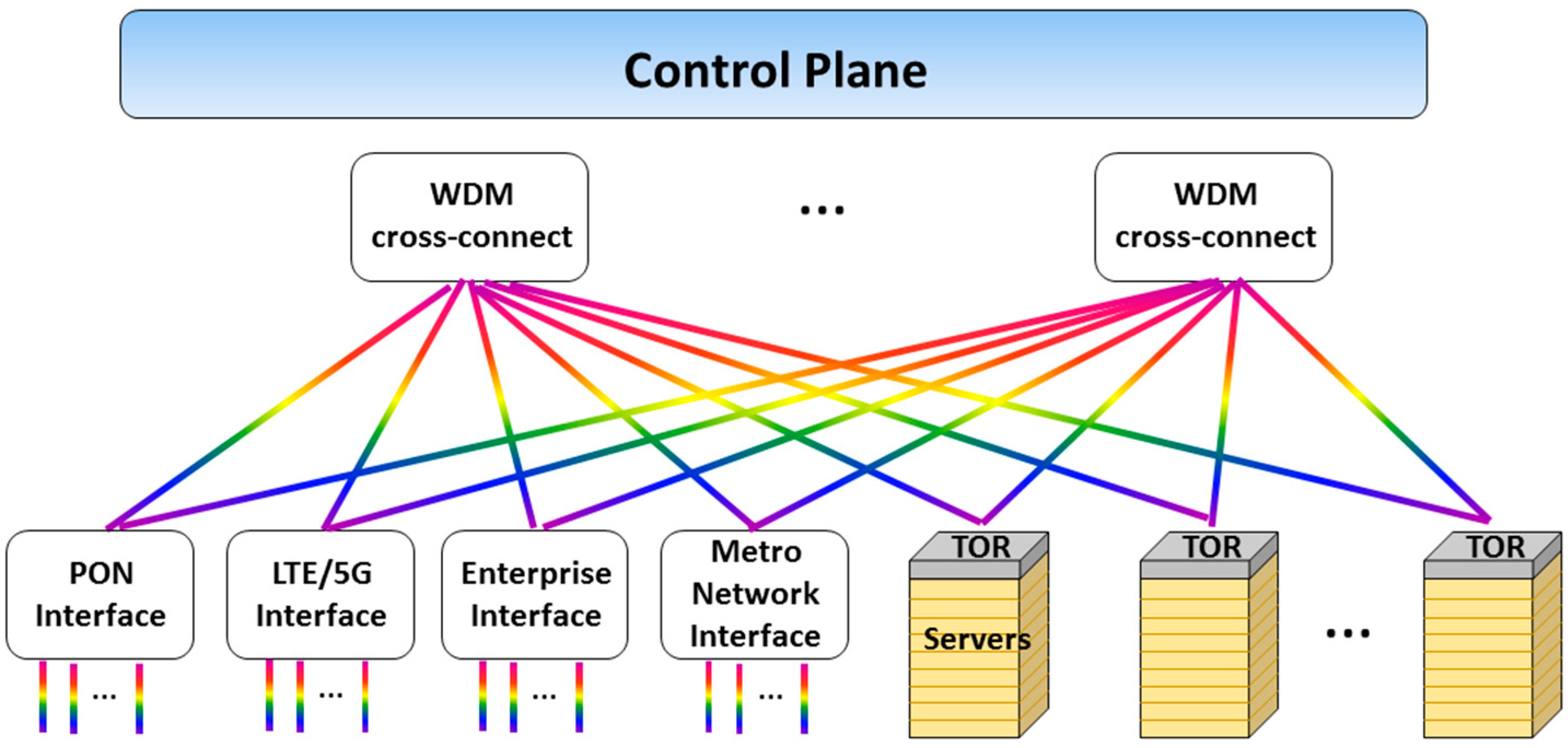
The optical metro node architecture exploiting the WDM cross-connects is reported in Figure 2. The optical node architecture include both optical and electrical (interfaces) switching. It consists of multiple interfaces (PON, LTE/5G, enterprise, metro network) that use multi-protocol, multilink interfaces, and hybrid electronic/optical switches to interface with access network segments along with the ability to mix and match protocols (i.e., CPRI, IP, Ethernet, etc.) over the same physical link. Moreover, the optical node includes also a number of servers organized in racks and interconnected via an electronic Top-of-the-Rack (TOR) switch. Each interface and TOR switch is equipped with a number of WDM bi-directional optical links. As shown in Figure 2, the interfaces and TORs are interconnected by a number of WDM cross-connect in a spine and leaf architecture. The main difference with the CORD approach is that the interconnect networks is built on a WDM cross-connect instead of electronic switches as in CORD. This allows to transparently switch the data traffic between the interfaces and the TORs without expensive O/E/O converters, greatly reducing the power consumption and costs. Moreover, the ability of the WDM cross-connect to switch data signals not only in wavelength and space, but also in time (at the nanosecond time scale), allows to fully exploit the statistical multiplexing switching at the optical data plane level. The number of interconnected interfaces and TORs and the capacity depends on the radix of the WDM cross-connect and the amount of parallel WDM cross-connect. For the PON, LTE/5G, and enterprise, the interface consists of the access interface and network interface, while for TOR it consists of a server interface and the network interface. Part of the traffic that belongs to the same access (the same PON or same server pool in the same rack) is then directly exchanged by the interfaces (or TORs). The other part of the traffic is directed to the network interface via multiple WDM transceivers, eventually with variable data rate and modulation formats. The reason for employing multiple WDM transceivers is that WDM allows scaling the communication bandwidth between the interfaces/TORs and the WDM cross-connect network employing multiple wavelengths to generate a high capacity channel. The control plane is, therefore, in charge of (re-)configuring the transceivers (data format and data rate) and, accordingly, the WDM cross-connects. As the main topic of this work is not the control plane and the implementation of the interfaces, the rest of the paper will discuss in detail and assess the design, photonic integration, and validation of the SOA-based WDM cross-connects.

3. SOA-Based WDM Cross-Connects

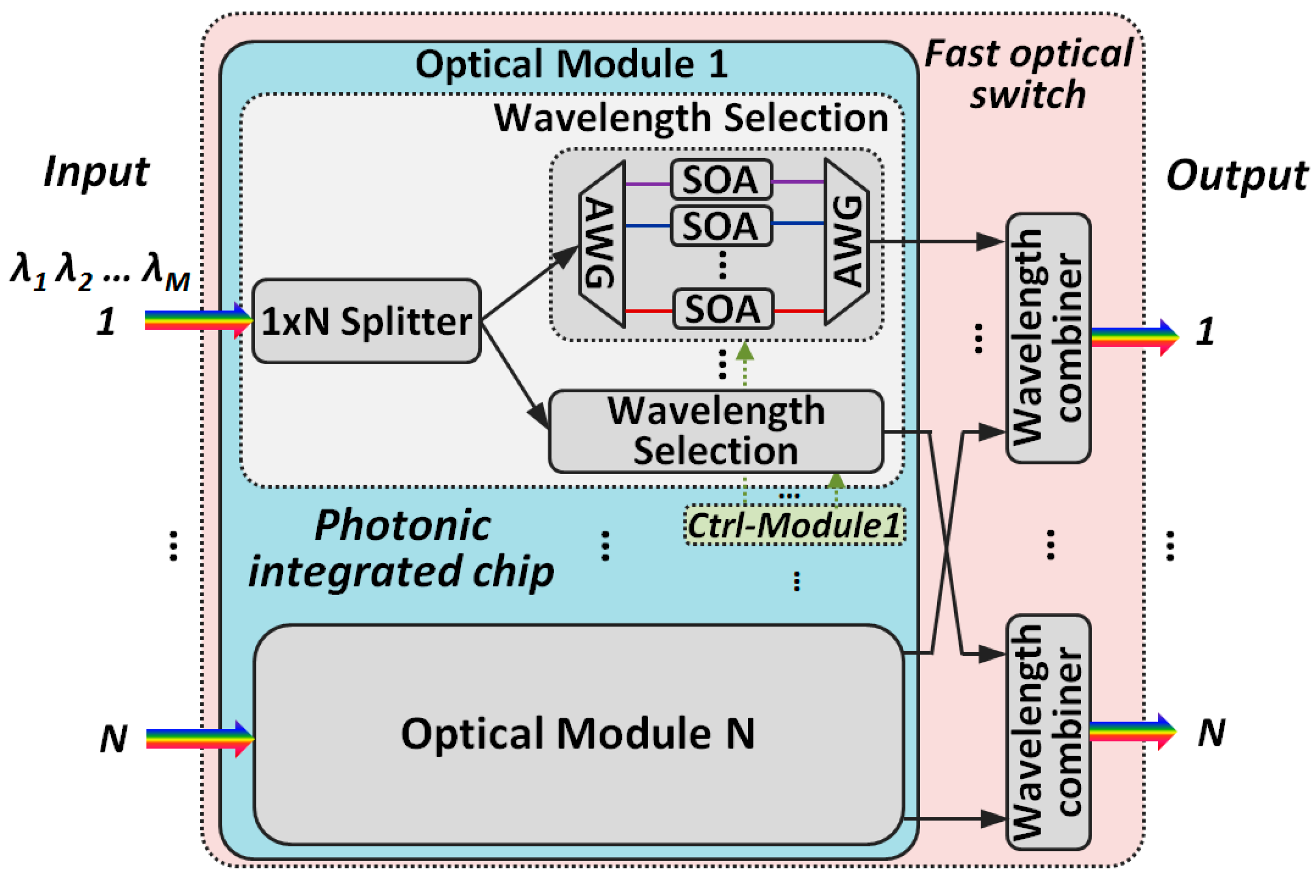
The schematic of the optical wavelength, space, and time cross-connect switch is illustrated in Figure 3. The non-blocking optical cross-connect has N inputs, and each input carries M different wavelengths generated by the interfaces/TORs. The modular cross-connect processes the N WDM inputs in parallel by the respective optical modules, and forwards the individual wavelength channels to any output ports according to the switching control signals provided by the control plane. A possible solution for fast (sub-microseconds) controlling of the switch is reported in [16]. Each optical module consists of a 1:N splitter to broadcast the WDM channels to the N wavelength selective switches (WSS). The outputs of the N WSSs are connected to the N wavelength combiners of the respective N output ports. Each WSS can select one or more wavelength channels and forward the channels to the output ports according to the control signals. The WSS consists of two AWGs (acting as a demultiplexer and a multiplexer) and M SOA based optical gates. The first 1xM AWG operates as wavelength demultiplexer. Turning on or off the M SOA optical gates determines which wavelength channel is forwarded to the output or is blocked. The second Mx1 AWG operates as a wavelength multiplexer. Multicast operation is also possible with this architecture. The broadband operation of the SOA enables the selection of any wavelength in the C band. Moreover, the amplification provided by the SOA compensates the losses introduced by the two AWGs. It should be noted that the amount of SOAs is NxNxM, but typically only NxM will be turned on. Moreover, during the switching operation, the modules operate in an independent and parallel way to each other, which introduces important features such as distributed control for the optical switch, leading to the following advantages. Firstly, the overall performance of the optical switch can be evaluated by testing a single module. Secondly, the parallel and independent operation of the module make the control complexity and the switching time (latency) of the entire switch independent of the port count and equal to the switching time of a single module. Furthermore, scaling the port count leads to a linear increase in components and energy consumption, by employing copies of the identical modules.

4. Photonic Integrated WDM Cross-Connect

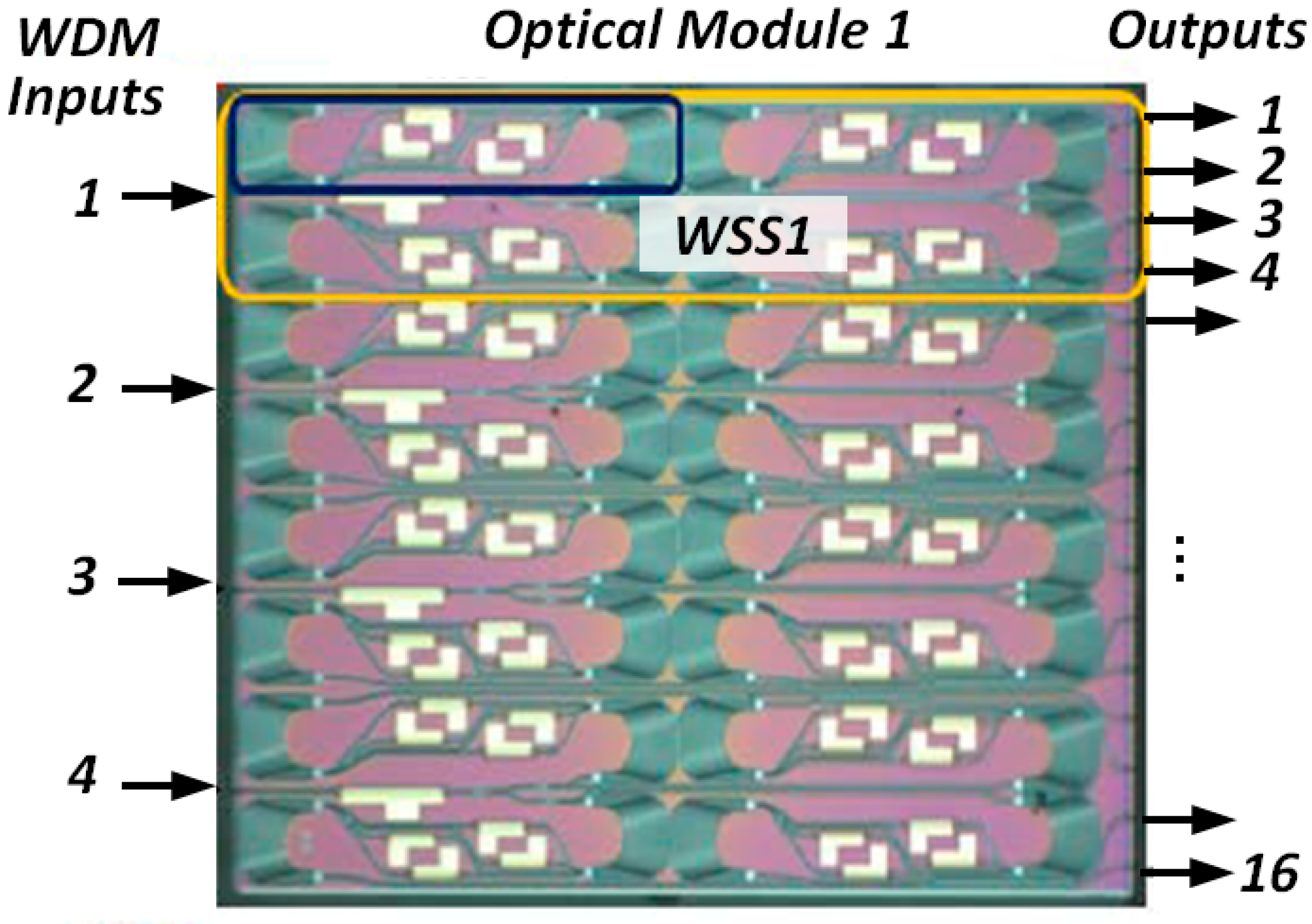
Based on the schematic shown in Figure 3, a PIC integrating four optical modules each with four WDM channels (without a wavelength combiner) are designed, as shown in Figure 4. The chip has been realized in a multi-project wafer (MPW) in the Jeppix platform with limited space of the cell (6 mm × 4 mm). Each of the four identical modules processes one of the four WDM inputs. At the input of each module, an 800 μm booster SOA is employed to compensate the 6 dB losses of the 1:4 splitter and, partially, the AWG losses at the WSS. The passive 1:4 splitter is realized by a cascading 1 × 2 multimode interferometer (MMI), with the outputs connected to four identical WSSs, respectively. The AWGs of the WSS are designed with a free spectral range (FSR) of 15 nm, which has been tailored to fit the limited cell size offered in the MWP. The quantum well active InGaAsP/InP SOA gates have a length of 350 μm. The input and output facets of the chip are anti-reflection coated. The chip includes a total of 112 elements (four booster SOA pre-amplifiers with DC bias, 64 gate SOAs with RF bias, 32 AWGs, and 12 1 × 2 MMI couplers). The light-shaded electrodes are wire bonded to the neighboring PCBs to enable the control of the SOA gates. Lensed fibers have been employed to couple the light in and out of the chip. Spectral tuning of the AWGs is, in principle, possible by using heaters on top of the AWG waveguides with a limited tuning range within the channel (not implemented in this design).
The parameters and static performances, including the operational bandwidth of the SOAs, central wavelength, as well as the passband for the AWGs, and crosstalk between different channels have been characterized by employing the experimental setup shown in Figure 5. Four optical input channels spaced by 500 GHz, from λ1 = 1532 nm to λ4 = 1544 nm, are launched into input port 1 of the photonic chip to characterize the chip. As the optical modules are identical, we have assessed the operation of one optical module to characterize the switching operation. The optical power of the WDM input channels was 2 dBm/channel (see also Figure 5). The input SOA was biased with 100 mA of current. The temperature of the chip was maintained at 25 °C. A polarization controller was employed at the input of the chip due to the high polarization-dependent loss of the quantum well SOAs.
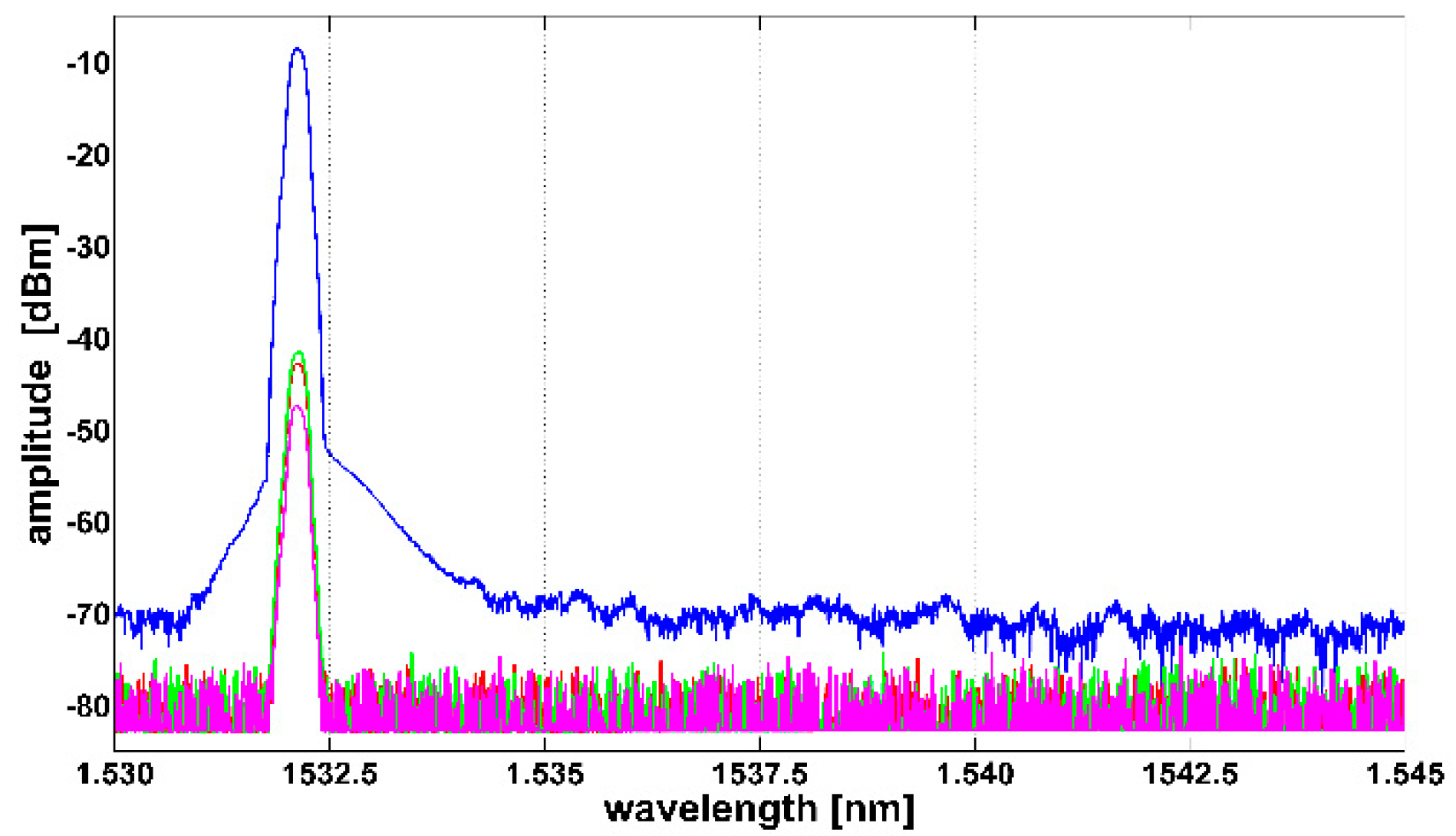
First we assess the operation of the single WSS. One WDM channel at a time is statically switched at the WSS output by enabling one of the four SOA gates at a time. The current applied at each of the SOA gates was 62 mA. The four measured spectra at the WSS output (output 1 of the chip) are shown in Figure 6. An on/off switch ratio higher than 30 dB was measured. The optical power at the chip output for Channel 1 and Channel 3 was −9 dBm. Considering 6 dB/facet coupling loss, a 1 dB on chip gain is estimated. However, Channels 2 and 4 have 10 dB of extra losses. Inspection of the chip reveals that two waveguides after the AWG demux are not fully resolved, which leads to substantial optical power coupling between the channels. The coupled signals at different wavelengths are filtered by the output AWG, explaining the extra losses. This can be solved in the next fabrication run.
In the second experiment, Channel 1 has been switched to one of the output ports at a time by enabling one of the SOA gates of the four WSSs at a time. To measure the cross-talk between the WSSs output ports (here we define the cross-talk as the ratio between the optical power of a single channel at the desired output port and the optical power at the other output ports), Figure 7 shows the optical spectra recorded at the four outputs when Channel 1 is only switched at output 1. A cross-talk <−30 dB was measured.
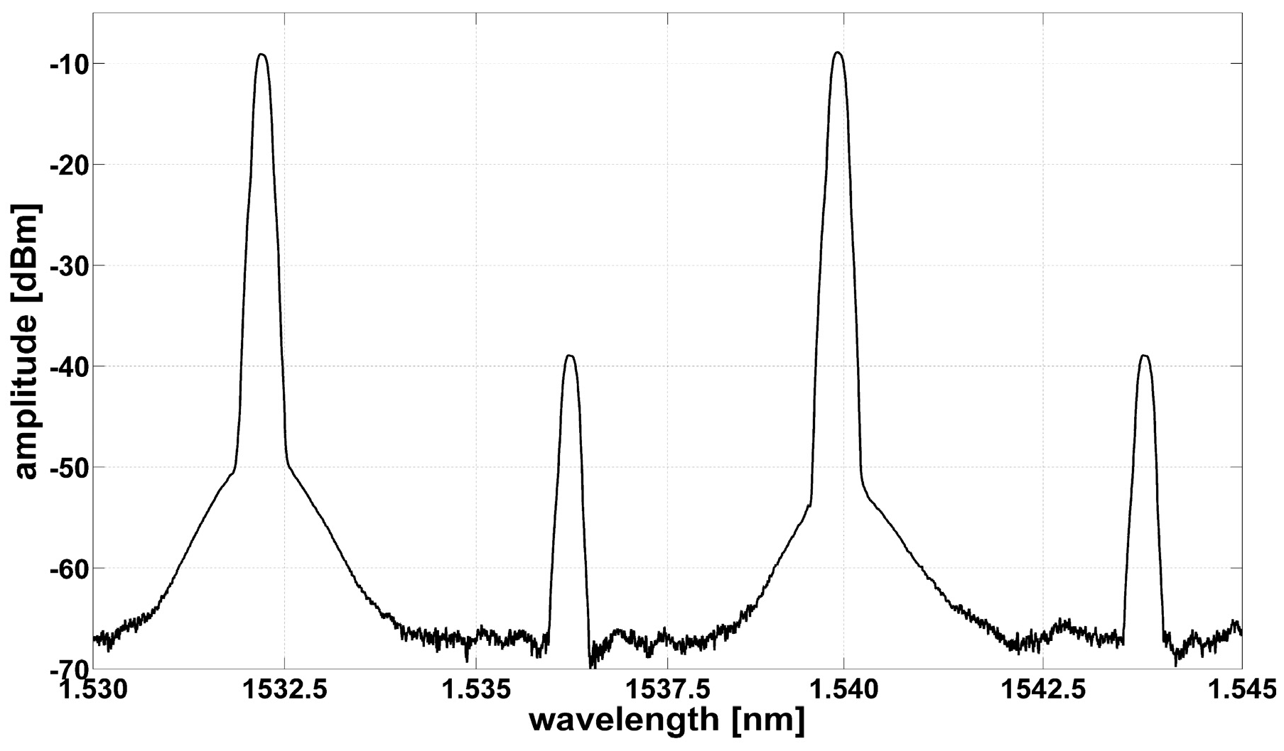
Furthermore, an experiment to validate the capability of the switch to forward multiple wavelengths in parallel was performed. In the setup, two SOA gates of the WSS2 for Channel 1 and Channel 3 are enabled to allow for both channels to be forwarded at output port 2. Figure 8 shows the recorded spectra at the output 2, clearly illustrating the forwarding of Channel 1 and Channel 3, while Channel 2 and Channel 4 are blocked, with a contrast ratio above 30 dB.

5. Experimental Results

To assess the performance of the 4 × 4 fast optical switch PIC, the experiment setup shown in Figure 5 is employed. Four WDM optical channels with packetized NRZ-OOK (PRBS 211-1) payloads at data rates of 10 Gb/s, 20 Gb/s, and 40 Gb/s are generated at 1525.0 nm, 1528.9 nm, 1532.9 nm, and 1536.8 nm. The packet has the duration of 540 ns and 60 ns guard time. The four WDM channels are de-correlated, amplified, and injected into the photonic-integrated WDM optical switch PIC via a polarization controller. Module 1, as one of the four identical modules, has been selected for the switching performance assessment. The total power launched into the input Port 1 is 2 dBm (corresponding to −4 dBm per channel). The input SOA, acting as a booster amplifier, is continuously biased with 100 mA of current. The shorter SOAs in the WSS acting as optical gates on the different channels are controlled by an FPGA-based switch controller.

5.1. Dynamic Switching

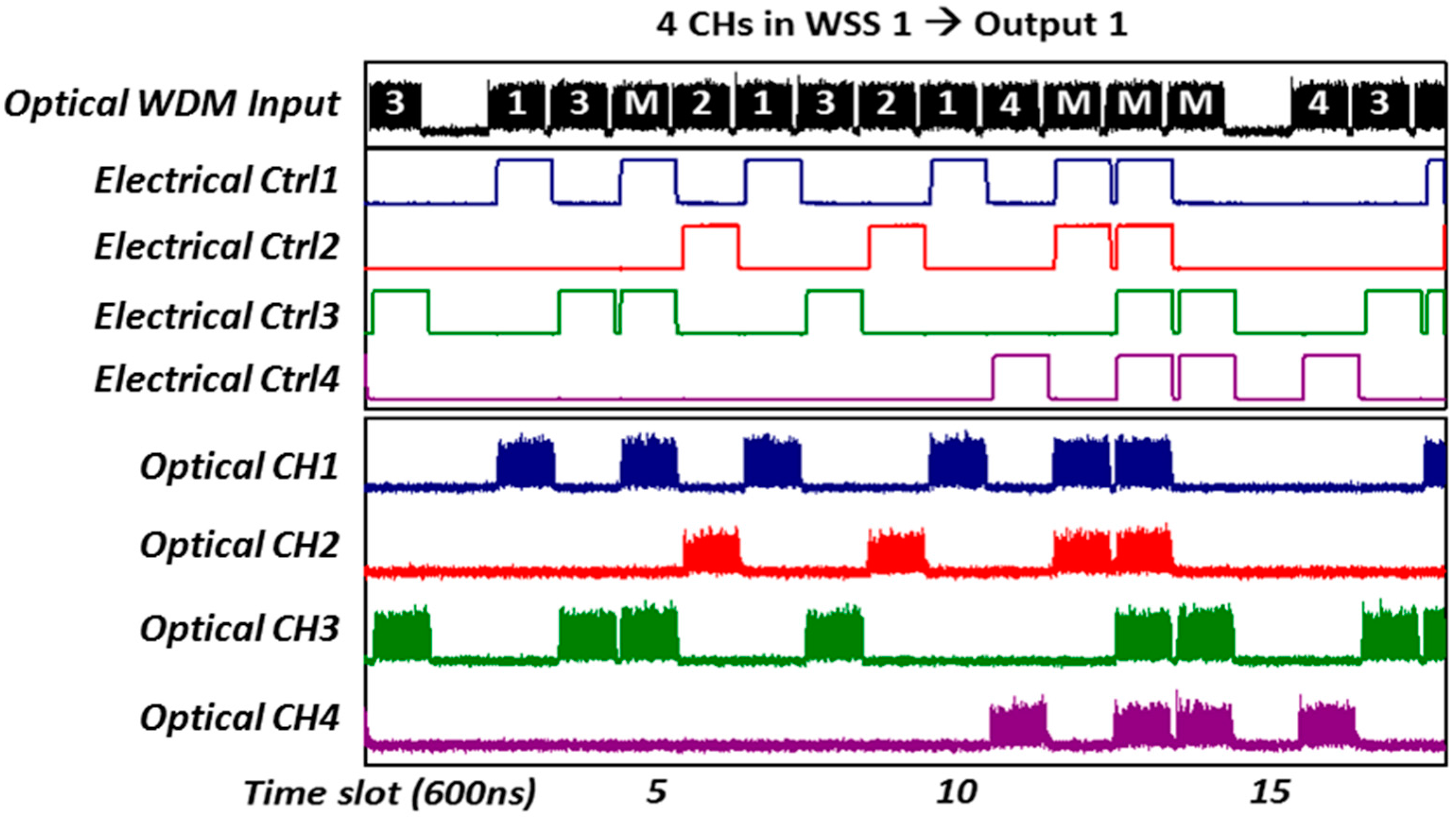
The dynamic switching operation of the single WSS (WSS1 in Figure 4) is first investigated. The WDM packets arriving at WSS 1 in Module 1 are de-multiplexed and controlled individually by the gate SOAs. The switch controller will turn on one or multiple gates to forward the packets, and the selected wavelength channels are multiplexed at the WSS output. The traces of the WDM input packets (shown in black) are illustrated in Figure 9. Each packet labelled with the wavelength channel needs to be switched to the Output 1, while packets labelled with “M” means that multiple gates are enabled for multicasting operation. The switch controls (Ctrl 1 to Ctrl4) generated by the FPGA and applied to the four SOA gates of the WSS are also illustrated in Figure 9. The signals are synchronized with the packets and “on” states correspond to a bias current of 40 mA. The packets of the four channels (CH 1–4) are fast switched (~10 nanoseconds) and the outputs are presented in Figure 9. The traces indicate that the packets are properly switched according to the control signals with a contrast ratio larger than 28 dB.
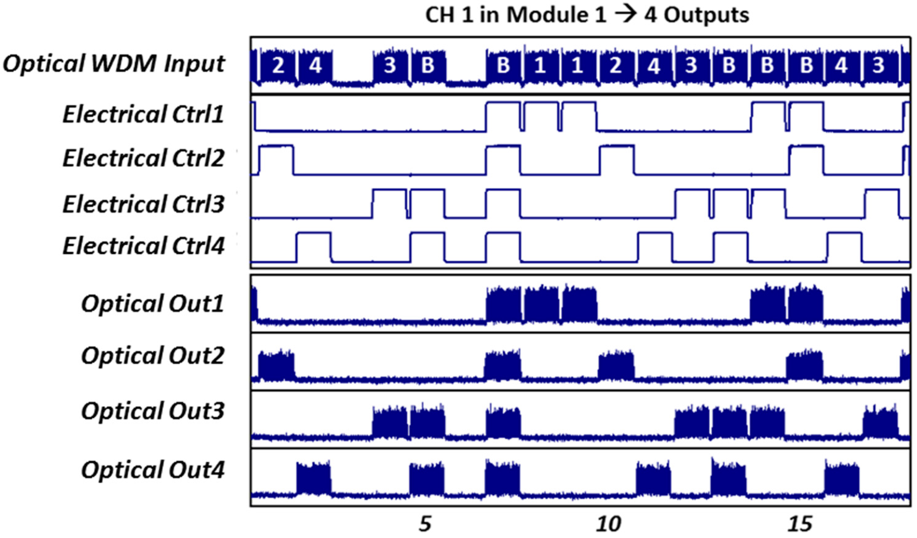
As a second system assessment, the dynamic switching operation of the four WSSs has been investigated. In this case, packets at wavelength Channel 1 (1525 nm) is switched to one of the four output ports by controlling the Channel 1 SOA gates of the four WSS. The traces of the input packets, the control signals, and the switched outputs are reported in Figure 10. The input packets are labelled with the destination output ports and broadcasting (“B”) to two or more ports is also enabled by turning on multiple SOA gates. It can be seen from Figure 10 that the fast dynamic switching operation in space, wavelength, as well as time domains are fully supported by the WDM fast optical switch PIC.
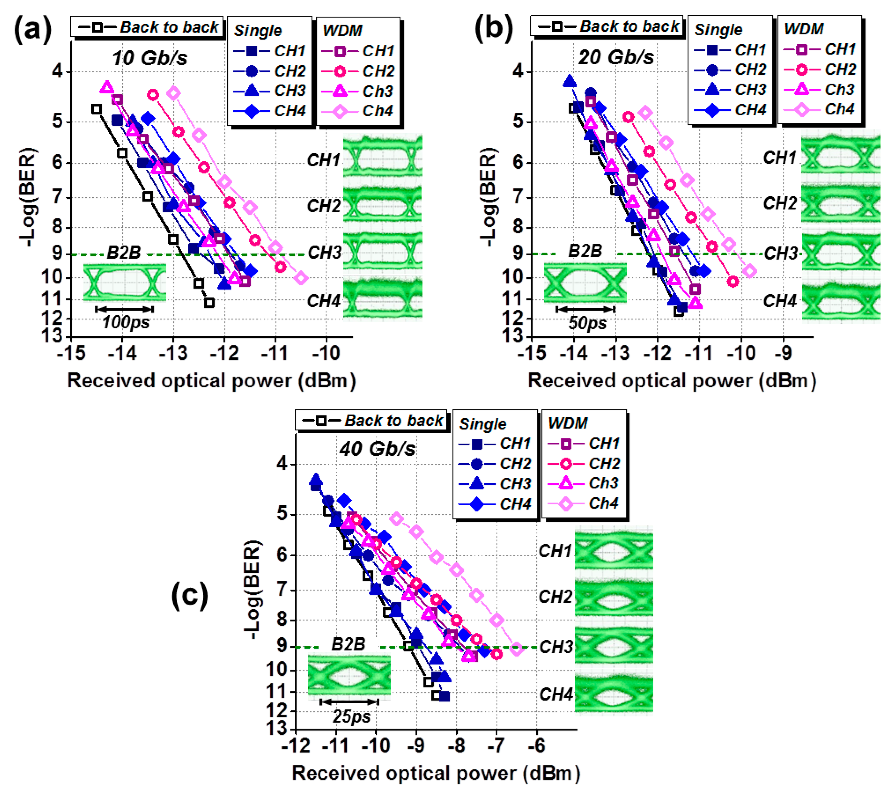
To quantify the performance of the fast optical switch PIC, the BER curves for each WDM channel at different data rates are measured and the results are shown in Figure 11a–c. The back-to-back (B2B) curves are also included for reference. The gate SOA for the channel under test is supplied with a 60 mA driving current and the output is amplified and sent to the BER tester (BERT). When the single wavelength channel is input to the PIC (shown in blue curves), error-free operations with less than 0.5 dB have been measured for Channel 1 (CH 1) and Channel 3 (CH 3) at different data rates while, for Channel 2 (CH 2) and Channel 4 (CH 4), the penalty was around 1 dB at 10 Gb/s, 20 Gb/s, and 2 dB at 40 Gb/s data rate. The eye diagrams of the switched output are also reported and confirm the signal degradation, mainly due to accumulated noise for CH 2 and CH 4. When all four WDM input channels are fed into the switch, the BER results (shown as red curves) indicate a slight performance degradation with an extra penalty of around 0.5 dB for CH 1 and CH 3 and 1 dB for CH 2 and CH 4 compared with single wavelength operation for the different data rates.
It can be seen from the assessment results that the WDM fast optical switch PIC can dynamically handle the WDM data traffic within a few nanoseconds in space and wavelength domains. Error-free operation has been measured for 10 Gb/s, 20 Gb/s, and 40 Gb/s in single, as well as multiple, WDM channels with <1.5 dB and <3 dB penalty for CH 1/3 and CH 2/4, respectively. As reported in the characterizations, CH 2 and 4 experience extra losses due to the substantial optical power coupling between the channels caused by the not fully resolved waveguides after the de-multiplexer AWG. Therefore, lower input power into the gate SOAs results in OSNR performance degradation, which is also confirmed by the BER curves and eye diagrams in Figure 11. The gain compensation brought by the SOAs and the resulting limited power penalty, indicates the potential scale of the PIC to higher data rates and port counts.

5.2. High-Data and Multi-Level Modulated Traffic

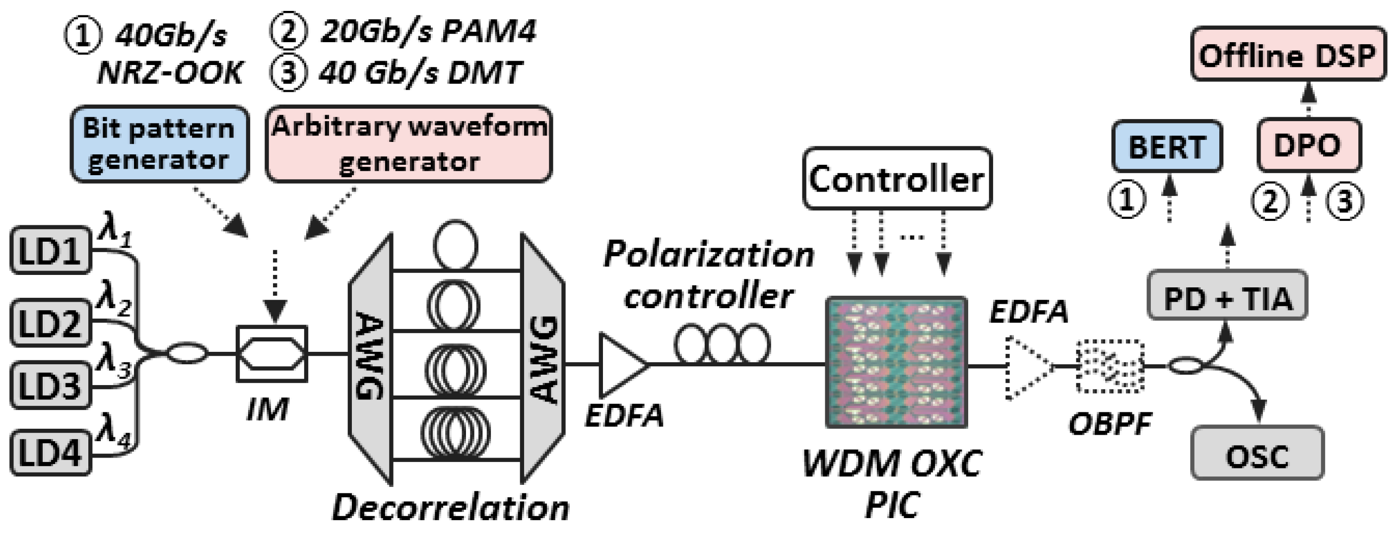
Considering the application of the fast optical switch PIC in DCNs deployed with advanced optical interconnect solutions, the capability of handling the high data-rate and multi-level modulated traffic is a necessity. The potential impact on the signal integrity and OSNR degradation when given lower input power, therefore, should be well addressed. To assess the performance of the fast optical switch PIC in switching the high-capacity and multi-level modulated traffic, the experimental setup shown in Figure 12 is employed. Three types of traffic are generated and tested, namely the 40 Gb/s NRZ-OOK, 20 Gb/s PAM4, and data-rate adaptive DMT. The four WDM channels are de-correlated, amplified, and polarization-controlled before reaching the fast optical switch PIC chip. Module 1, as one of the four identical modules, has been selected for the switching performance assessment. The bias current for the booster SOA and gate SOA are adjusted by an FPGA-based switch controller.
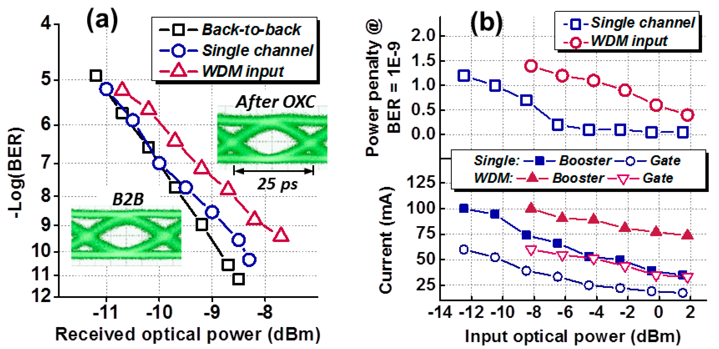
The switching of the packetized 40 Gb/s NRZ-OOK (PRBS 211-1) traffic is first analyzed. The power of each channel launched into the WDM OXC is −4 dBm and the driving current for the booster SOA and gate SOA are 100 mA and 60 mA, respectively. At the output, switched traffic is amplified and sent to the BER tester (BERT). The BER curves, as well as eye diagrams for Channel 1 with a single channel and WDM input applied are shown in Figure 13a. The back-to-back (B2B) curve is also included for reference. Error-free operation with a 0.5 dB power penalty at a BER of 1 × 10⁻⁹ has been measured for single channel case. When four WDM channels are fed into the switch, the result indicates slight performance degradation with a penalty of around 1 dB which is mainly due to the noise introduced by the SOAs. The power penalty measured at BER of 1 × 10⁻⁹ with different input optical power is plotted in Figure 13b. The bias current for the booster and gate SOAs are varied to equalize the output power of the chip. For single channel input, 14 dB dynamic range is achieved with less than 1.5 power dB penalty. WDM input would cause an expense of 1 dB extra penalty. A smaller dynamic range of 10 dB is obtained for the WDM input case. The required bias current for the booster SOA and gate SOA is also illustrated in Figure 13b. Higher input power would require less driving current for both SOAs to achieve the equalized power output.
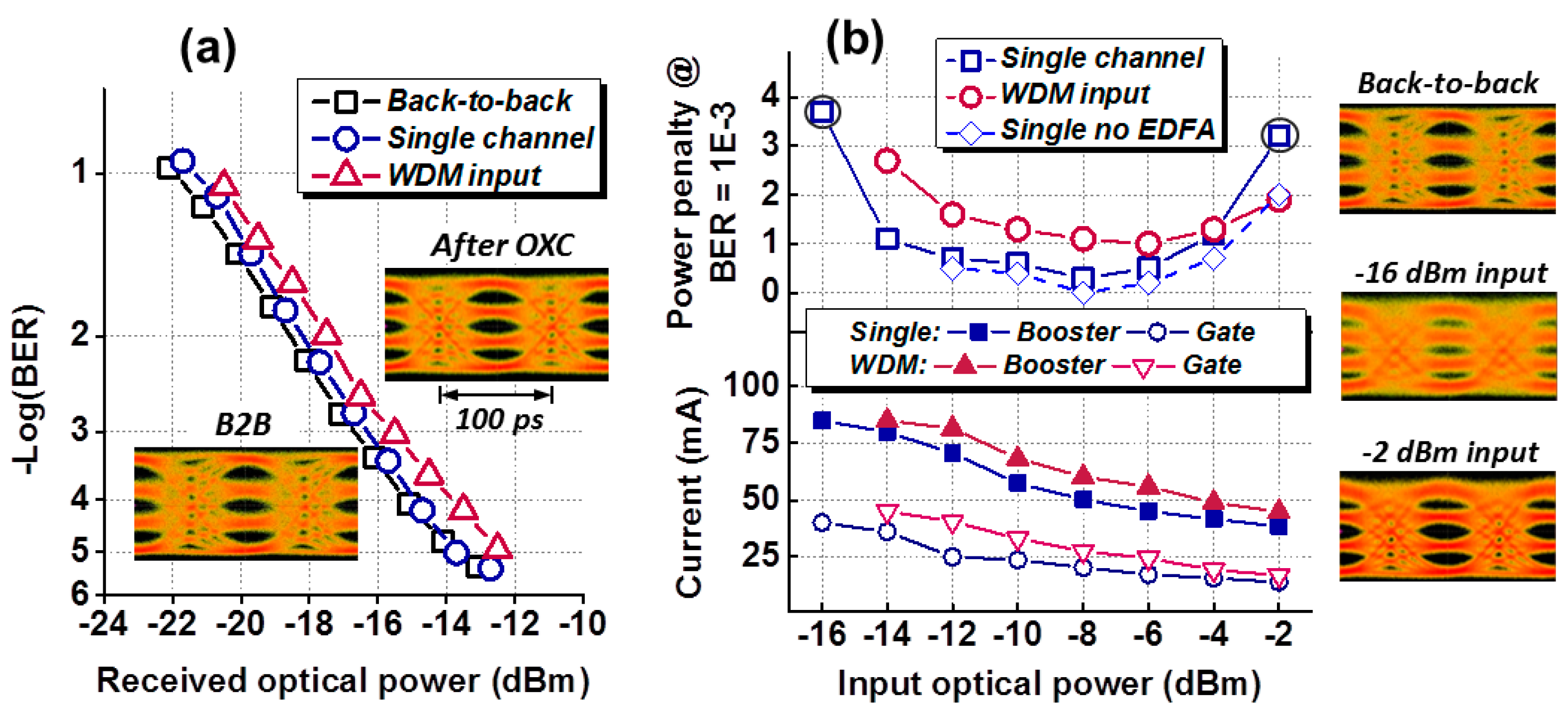
As promising interconnect solutions, PAM4 and DMT can effectively boost the link capacity, and the switching performances have been analyzed for the fast optical switch PIC. The WDM channels are modulated with the PAM4 and DMT traffic generated by the 24 GSa/s arbitrary waveform generator. At the switch output, the traffic is received by a real-time 50 GSa/s digital phosphor oscilloscope (DPO) for offline DSP. The BER curves and the eye diagrams of the switched 20 Gb/s PAM4 traffic at Channel 1 are shown in Figure 14a. A power penalty of 0.4 dB and 1 dB at BER of 1 × 10⁻³ has been observed for the single channel and WDM input, respectively. The optical power dynamic range guaranteeing a BER < 1 × 10⁻³ is then studied. The power penalty when varying the input power and the corresponding bias current of both SOAs for equalized output are depicted in Figure 14b. Both cases achieve >10 dB dynamic range within a 2 dB power penalty. Similar to the NRZ-OOK traffic, lower input power is limited by the OSNR degradation where the noise is more dominant. A larger penalty is also found for higher input power due to the increased sensitivity to saturation, as confirmed by the eye diagrams in Figure 14b. The situation without the output EDFA is also investigated for the single channel input case, and the dynamic range result is presented in Figure 14b. A similar trend with a smaller power penalty has been observed compared to the presence of EDFA. A smaller dynamic range is mainly due to the inadequate output power level when lower input power is applied.
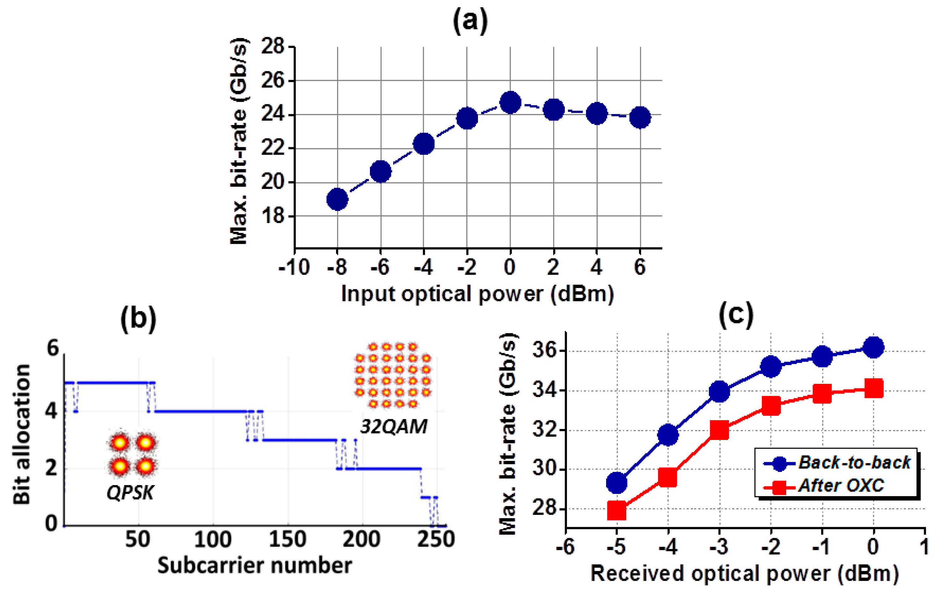
For the DMT traffic, we first evaluated the effect of the input power to the optical switch PIC chip on the achievable data-rate. As illustrated in Figure 15a, 0 dBm is found to be the optimum (absolute data-rate is not optimized). An example of the optimal bit allocation after bit loading for the 10 GHz DMT with 256 sub-carriers is included in Figure 15b. Channel 1 with 0 dBm optical power is sent to the PIC and the maximum achievable data-rate with an average BER < 1 × 10⁻³ is reported in Figure 15c. A 1 dB penalty in the data-rate of 32 Gb/s is introduced by the WDM optical switch PIC compared with the B2B traffic.

6. Conclusions

We presented the assessment of a photonic integrated WDM optical cross-connect as one of the main building blocks for interconnecting network elements, as well as computing and storage resources implemented in an optical metro node architecture. The photonic WDM cross-connect node based on semiconductor optical amplifiers (SOA) allows switching data signals in wavelength, space, and time for fully exploiting statistical multiplexing. The assessment of a 4 × 4 photonic WDM cross-connect in terms of switching speed, photonic integrated amplification for loss-less operation, and gain equalization has been reported. The experimental results confirm the potential lossless operation, large optical power dynamic range, low cross-talk <−30 dB, and multicasting operation. Compensation of the losses is a good indication that the modular architecture could scale to a larger number of ports. Moreover, the assessment of the cross-connect switch with multiple WDM channels and diverse modulation formats indicate dynamically switching within a few nanoseconds the WDM data packets and error-free operation with less than a 2 dB power penalty for single channel, as well as WDM input operation, for multiple 10/20/40 Gb/s NRZ-OOK, 20 Gb/s PAM4, and data-rate adaptive DMT traffic.
Considering the practical implementation, due to the identical modular structure, the scalability of the WDM cross-connect switch is mainly determined by possible AWG crosstalk degradation with the increase of the number of ports and by the broadcast and select optical switch. On the AWG crosstalk, it has been demonstrated the potential to have a large (>64) number of ports with very slight degradation of the crosstalk. The splitting loss caused by the broadcasting stage can be compensated by the SOA gates, guaranteeing loss-less operation and sufficient power level for the receiver side, the noise added by the SOA will lead to an OSNR degradation. Therefore, the main limiting factor of scaling out the port-count beyond 64 ports is the OSNR degradation due to the splitting loss experienced by the optical data.

Acknowledgments

The authors would like to thank H2020 METRO-HAUL project (grant number 761727) for supporting this work, and JePPIX for the chip fabrication.

Author Contributions

Nicola Calabretta conceived and designed the PIC WDM cross-connect and wrote the paper. Wang Miao, Ketemaw Mekonnen and Kristif Prifti performed the experiments and analyzed the data with Nicola Calabretta.

Conflicts of Interest

The authors declare no conflict of interest.

References

  1. Cisco Systems. Cisco Global Cloud Index: Forecast and Methodology 2014–2019; Cisco Systems: San Jose, CA, USA, 2015. [Google Scholar]
  2. CORD Project. Available online: http://opencord.org/ (accessed on 12 June 2017).
  3. De Leenheer, M.; Tofigh, T.; Parulkar, G. Open and Programmable Metro Networks. In Proceedings of the Optical Fiber Communication Conference and Exhibition 2016, Anaheim, CA, USA, 20–24 March 2016. [Google Scholar]
  4. Napoli, A.; Bohn, M.; Rafique, D.; Stavdas, A.; Sambo, N.; Poti, L.; Nölle, M.; Fischer, J.K.; Riccardi, E.; Pagano, A. Next generation elastic optical networks: The vision of the European research project IDEALIST. IEEE Commun. Mag. 2015, 53, 153–162. [Google Scholar] [CrossRef]
  5. Ruffini, M. Metro-Access Network Convergence. In Proceedings of the Optical Fiber Communication Conference and Exhibition 2016, Anaheim, CA, USA, 20–24 March 2016. [Google Scholar]
  6. H2020 METRO-HAUL Project. Available online: https://metro-haul.eu (accessed on 21 June 2017).
  7. Ghiasi, A. Large data centers interconnect bottlenecks. Opt. Express 2015, 23, 2085–2090. [Google Scholar] [CrossRef] [PubMed]
  8. Tucker, R. How to build a petabit-per-second optical router. In Proceedings of the 19th Annual Meeting IEEE Lasers Electro-Optics Society, Montreal, QC, Canada, 29 October–2 November 2006; pp. 486–487. [Google Scholar]
  9. DeCusatis, C. Optical Interconnect Networks for Data Communications. J. Lightwave Technol. 2014, 32, 544–552. [Google Scholar] [CrossRef]
  10. Kachris, C.; Tomkos, I. A Survey on Optical Interconnects for Data Centers. IEEE Commun. Surv. Tutor. 2012, 14, 1021–1036. [Google Scholar] [CrossRef]
  11. Farrington, N.; Porter, G.; Sun, P.-C.; Forencich, A.; Ford, J.; Fainman, Y.G.; Papen, G.; Vahdat, A. A demonstration of ultra-low-latency data center optical circuit switching. Comput. Commun. Rev. 2012, 42, 95–96. [Google Scholar] [CrossRef]
  12. Hemenway, R.; Grzybowski, R.; Minkenberg, C.; Luijten, R. Optical-packet-switched interconnect for supercomputer applications. J. Opt. Netw. 2004, 3, 900–913. [Google Scholar] [CrossRef]
  13. Liboiron-Ladouceur, O.; Shacham, A.; Small, B.A.; Lee, B.G.; Wang, H.; Lai, C.P.; Biberman, A.; Bergman, K. The data vortex optical packet switched interconnection network. J. Lightwave Technol. 2008, 26, 1777–1789. [Google Scholar] [CrossRef]
  14. Ye, X.; Yin, Y.; Yoo, S.J.B.; Mejia, P.; Proietti, R.; Akella, V. DOS: A scalable optical switch for datacenters. In Proceedings of the 6th ACM/IEEE Symposium on Architectures for Networking and Communications Systems, La Jolla, CA, USA, 25–26 October 2010. [Google Scholar]
  15. Yan, F.; Miao, W.; Dorren, H.J.S.; Calabretta, N. Novel flat DCN architecture based on optical switches with fast flow control. In Proceedings of the International Conference on Photonics in Switching (PS), Florence, Italy, 22–25 September 2015; pp. 309–311. [Google Scholar]
  16. Miao, W.; Luo, J.; di Lucente, S.; Dorren, H.; Calabretta, N. Novel flat datacenter network architecture based on scalable and flow-controlled optical switch system. Opt. Express 2014, 22, 2465. [Google Scholar] [CrossRef] [PubMed]
Figure 1. Target hardware built from commodity servers, I/O blades, and switches.
Applsci 07 00865 g001
Figure 2. Optical metro node architecture exploiting the Wavelength Division Multiplexing (WDM) cross-connects.
Applsci 07 00865 g002
Figure 3. Schematic of the WDM cross-connect based on Semiconductor Optical Amplifiers (SOAs).
Applsci 07 00865 g003
Figure 4. Schematic of the fabricated 4 × 4 fast optical switch PIC.
Applsci 07 00865 g004
Figure 5. Experimental setup employed to assess the performance of the WDM photonic cross-connect.
Applsci 07 00865 g005
Figure 6. Optical spectra of the WDM channels switched by the Wavelength Selective Switch (WSS).
Applsci 07 00865 g006
Figure 7. Recorded spectra of Channel 1 at the four WSS outputs (only the SOA gate of WSS1 was enabled).
Applsci 07 00865 g007
Figure 8. Optical spectra recorded at output port 2 showing the WDM switching operation of the photonic chip.
Applsci 07 00865 g008
Figure 9. Traces for four channels in WSS1 destined to Output 1.
Applsci 07 00865 g009
Figure 10. Traces for Channel 1 in Module 1 destined to four outputs.
Applsci 07 00865 g010
Figure 11. BER curves for single channel and WDM channel input at (a) 10 Gb/s; (b) 20 Gb/s; and (c) 40 Gb/s.
Applsci 07 00865 g011
Figure 12. Experimental setup for the performance assessment of NRZ-OOK traffic.
Applsci 07 00865 g012
Figure 13. (a) BER curves and (b) the dynamic range with adjusted SOA current for 40 Gb/s traffic.
Applsci 07 00865 g013
Figure 14. (a) BER curves and (b) the dynamic range with adjusted SOA current for 20 Gb/s PAM4 traffic.
Applsci 07 00865 g014
Figure 15. (a) Optimal input power; (b) bit allocation per subcarrier; and (c) maximum data-rate with different received optical powers for DMT traffic.
Applsci 07 00865 g015