All-Carbon Electrodes for Flexible Solar Cells


1
State Key Laboratory of New Ceramics and Fine Processing, School of Materials Science and Engineering, Tsinghua University, Beijing 100084, China
2
Key Laboratory of Advanced Materials (MOE), School of Materials Science and Engineering, Tsinghua University, Beijing 100084, China
3
School of Physics and Electronic Engineering, Xinjiang Normal University, Urumqi 830046, Xinjiang Province, China
4
Qian Xuesen Laboratory of Space Technology, China Academy of Space Technology, Beijing 100094, China
5
Graduate School at Shenzhen, Tsinghua University, Shenzhen 518055, Guangdong Province, China
*
Authors to whom correspondence should be addressed.
Appl. Sci. 2018, 8(2), 152; https://doi.org/10.3390/app8020152
Submission received: 16 December 2017
/
Revised: 8 January 2018
/
Accepted: 20 January 2018
/
Published: 23 January 2018
(This article belongs to the Special Issue Nanostructured Photodetectors and Photovoltaic Devices)
Abstract
:Transparent electrodes based on carbon nanomaterials have recently emerged as new alternatives to indium tin oxide (ITO) or noble metal in organic photovoltaics (OPVs) due to their attractive advantages, such as long-term stability, environmental friendliness, high conductivity, and low cost. However, it is still a challenge to apply all-carbon electrodes in OPVs. Here, we report our efforts to develop all-carbon electrodes in organic solar cells fabricated with different carbon-based materials, including carbon nanotubes (CNTs) and graphene films synthesized by chemical vapor deposition (CVD). Flexible and semitransparent solar cells with all-carbon electrodes are successfully fabricated. The best power conversion efficiency achieved for the devices with all-carbon electrodes is 0.63%, comparable to the reported performance of OPVs using pristine CVD graphene films as anodes on rigid substrates (glass). Moreover, the current densities of as-obtained devices are comparable to those assembled with all-carbon active layers and standard electrodes (e.g., ITO and metal), which indicates that the all-carbon electrodes made of CNT and graphene films are suitably effective for carrier collection and extraction. Our results present the feasibility and potential of applying all-carbon electrodes based on graphitic nanomaterials in next-generation carbon-based photovoltaics.
1. Introduction
Carbon materials including zero-dimensional fullerenes [1], one-dimensional carbon nanotubes (CNTs) [2], and two-dimensional graphene [3] have attracted increasing attention due to their unique physical, chemical, and electrical properties. They inspire scientists to attempt to collect them to assembly all-carbon optoelectronic devices, including photodetectors [4,5] and photovoltaics [6,7,8,9,10,11,12,13,14,15,16], which have many potential advantages, such as low cost, simple processing, and long-term stability. Currently, in the field of photovoltaics, carbon nanomaterials are mainly employed as additives [17,18,19,20,21,22,23] or transparent electrodes [24,25,26,27,28,29,30,31,32,33,34,35,36,37,38]. Organic photovoltaics (OPVs) have special advantages including light weight, good flexibility, convenient fabrication, and large-area feasibility, which make them versatile in niche places unfit for Si-based inorganic solar cells, such as power-generating windows and flexible electronic devices [39,40]. Yang’s group reported visibly transparent OPVs that have a maximum transparency of 66% at 550 nm, aimed to be add-on components of multijunction photovoltaics, smart windows, and building-integrated photovoltaics (PVs) [41]. However, almost all published OPV devices require the use of a metal oxide (e.g., indium tin oxide, ITO) and noble metals (e.g., Ag, Au) as electrode materials, both of which have some drawbacks, as the former is brittle and expensive, the latter is reflective and opaque. These material issues are being addressed by the development of transparent and flexible thin films made of carbon nanostructures including CNTs and graphene. Some studies have been carried out with CNTs and graphene as anodes in OPV cells. In 2006, Rowell et al. used printed films of single-walled carbon nanotube networks on plastic as transparent and flexible anodes of OPVs with a power conversion efficiency (PCE) close to the performance of its ITO/glass counterpart [42]. CNT films produced by chemical vapor deposition (CVD) [31,43], polyaniline interfacial polymerization [29], and brush-painting [44] were also employed as anodes for building ITO-free OPVs, showing more flexible properties than their ITO-based counterparts. Meanwhile, researchers also tried to apply graphene as anodes. For example, large-area graphene films synthesized via CVD were successfully used as anodes in OPV cells, showing the potential of graphene to replace ITO [45]. Chemically reduced graphene oxide was another material employed to form graphene flexible electrodes through spin-casting onto substrates [33,46,47]; however, its low optical transmittance and high sheet resistance were generally not favorable to the fabrication of solar cells with high efficiency. Thus, the CVD process is preferable for the preparation of thin films with a large area, intact structure, and low number of defects for either CNT or graphene. Concerning cathodes, CNT and graphene films were used to substitute the conventional metal grid combined with ITO; consequently, it became possible to fabricate semi-transparent OPVs that could be illuminated at both sides [26,31,48]. However, carbon-based flexible electrodes are applied only on one side of abovementioned OPVs, which still involve brittle ITO or noble metals. Recently, graphene anode- and cathode-based OPVs have been demonstrated, paving the way to flexible solar cells with full graphene electrodes [35,37,38]. To date, there are relatively few studies devoted to all-carbon electrode applications in OPVs. In this context, it is promisingly cost-effective to replace metal oxide- and metal-based electrode materials with flexible transparent carbon-based nanomaterials as electrodes in OPVs [49,50].
In this work, CNT and graphene films are used as both anodes and cathodes in conventional OPVs. The large-area, continuous, and highly transparent CNT and graphene films were synthesized and transferred onto flexible substrates. These thin films were investigated by multiple characterizations to estimate their applicability as electrode materials. Using few-layer graphene films on polyethylene naphthalate (PEN) as bottom electrodes, as well as few-layer or multi-layer graphene films or CNT thin films as top electrodes, flexible and semitransparent OPV devices with all-carbon electrodes were assembled and evaluated.
2. Materials and Methods
2.1. Synthesis and Transfer of CNT and Graphene Films
Large-area graphene films were grown by CVD using methane as a carbon resource and copper foils as substrates (25 μm in thickness, Alfa Aesar, Heysham, UK). Graphene transfer was carried out by spin-coating polymethyl methacrylate (PMMA) and the copper foil was etched away in a mixed solution of FeCl3/HCl, followed by rinsing with deionized water several times. Then the PMMA-supported graphene films were transferred onto a pre-patterned and cleaned PEN substrate. The PMMA was/was not removed by rinsing with acetone and isopropyl alcohol (IPA) when the graphene film were used as cathodes/anodes. Large-area and free-standing CNT films were synthesized by the CVD method using xylene (carbon source) and ferrocene (catalyst) as precursors, a gas mixture of Ar and H2 as the carrier gas, and nickel foil as the collector, which is detailed in our previous work [34]. The purification process of CNT films contained three steps: first, it was washed in hydrogen peroxide (H2O2, 30%) for 72 h to remove amorphous carbon, then soaked in hydrochloric acid (HCl, 36.5%) for 4~5 h to remove the iron catalyst residue, and finally washed with deionized (DI) water three times.
2.2. Synthesis of ZnO Nanoparticles
Zinc acetate dihydrate (2.36 g) was dissolved in methanol (100 mL) with stirring at 73 °C. A solution of KOH (1.26 g) in methanol (52 mL) was then slowly added over a period of 10 min. The reaction mixture was stirred for 2.5 h at 73 °C. After cooling to room temperature, the supernatant was decanted and the precipitate was washed twice with methanol (20 mL). Using n-butanol (50 mL) and methanol (2 mL) to disperse the precipitate and finally obtain a ZnO nanoparticle solution, the images of which by transmission electron microscope are shown in Figure S1. The ZnO nanoparticle solution was filtered through a 0.45-μm polyvinylidene fluoride (PVDF) syringe filter before use.
2.3. OPVs Assembly and Evaluation
OPV cells were fabricated on G/PEN substrates in an Ar-purged glovebox (0.1 ppm O2 and H2O). First, the ZnO nanoparticle solution was spin-coated onto the G/PEN substrates at 3000 r/min for 50 s. This procedure was repeated twice to obtain a continuous smooth film and then baked at 120 °C for 10 min. After drying, 20 mg of poly(3-hexyl)thiophene (P3HT, regioregular, Sigma-Aldrich, St. Louis, MO, USA) and 16 mg of phenyl-C61-butyricacid methyl ester (PCBM, Sigma-Aldrich, St. Louis, MO, USA) were dissolved in 1 mL of chlorobenzene to obtain a P3HT:PCBM mixed solution, which was spin-coated on the top of ZnO/G/PEN at 3000 r/min for 1 min as the active layer and subsequently dried at 120 °C for 10 min. Then the following steps were processed in the ambient conditions. The poly(3,4-ethylenedioxythiophene):poly(styrenesulfonate) (PEDOT:PSS) (1.3 wt % dispersion in H2O with conductive grade, Sigma-Aldrich, Samoa, USA) solution (mixed with 5 wt % isopropyl alcohol and 1 wt % surfactant (Zonyl-FSH, Dupont, Wilmington, DE, USA) and filtered through a 0.45-μm filter) was spin-coated onto the active layer at 3000 r/min for 50 s. Finally, the PMMA/G or CNT films were transferred onto the devices as the top contact. In a natural atmosphere, the photovoltaic properties were measured under Air Mass 1.5 (AM 1.5) illumination (100 mW/cm2) and the current-voltage data were recorded by a Keithley 4200 SourceMeter (Tektronix, Beaverton, OR, USA). The efficient area of all devices was controlled by a circular mask with a diameter of 3 mm.
2.4. Characterization
Optical transmittance spectra of CNT and graphene films were collected by a UV-2450 UV/vis optical spectrometer (Shimadzu, Kyoto, Japan). The sheet resistance of these films were measured using a four-probe resistivity test system. Raman spectra were obtained with a Renishaw 2000 Raman system (Renishaw, London, UK) with a 514 nm laser. Optical photographs were obtained by an optical microscope (Axio Scope A1, Zeiss, Oberkochen, Germany). The surface flatness of CNT and graphene films were investigated using an atomic force microscope (AFM, Agilent 5100, Agilent, Palo Alto, CA, USA). The morphologies of CNT and graphene samples were characterized using a transmission electron microscope (TEM, JEM-2010, JEOL, Tokyo, Japan).
3. Results
3.1. Fabrication and Energy Band of Solar Cells with All-Carbon Electrodes
First of all, to evaluate the feasibility of carbon-based film materials as all-carbon electrodes, CVD graphene and CNT films were used to fabricate OPV cells. The mixture of C60-based derivative (phenyl-C61-butyricacid methyl ester: PCBM) and P3HT (poly(3-hexyl)thiophene) [39] was employed as an active layer to absorb incident radiation and generate excitons. The schematic diagram of our devices is shown in Figure 1a. Graphene films were firstly transferred onto a flexible PEN wafer as bottom electrodes, and then ZnO nanoparticles were spin-coated as an electron transport layer [51]. In order to gain homogeneously dispersed nanoparticles, this step was repeated twice. After the active layer and hole transport layer of poly(3,4-ethylenedioxythiophene):poly(styrenesulfonate) (PEDOT:PSS) were coated, CNT or G films were laminated as the top transparent electrode. In the energy band diagram shown Figure 1b, the work functions of CNT and graphene films are set to 4.7 eV, depending on their thickness and purity [36,52]. On the top side, i.e., the anodes, the energy band of CNT and graphene films is near to that of ITO, which is slightly lower than the highest occupied molecular orbital (HOMO) of PEDOT:PSS. This match is favorable to extract and collect holes to the external circuit. The whole energy band diagram theoretically indicates that it is viable to use all-carbon electrodes in this structure. Semitransparent and flexible solar cells with all-carbon electrodes are shown in Figure 1c,d. It is indispensable to use transparent and flexible PV devices in some applications, such as power-generating windows and portable electronic devices. So, there are structural advantages to using two-dimensional carbon nanomaterials as electrodes in solar cells.
3.2. Preparation and Characterization of Graphene Films
Next, for transparent conductive electrodes in thin-film carbon-based solar cells, large-area and high-quality carbon-based films are needed. Thus, we used the CVD method to synthesize large-area graphene and CNT films. Because there is a trade-off between transparency and conductivity for graphene films, to gain more insight about this balance, few-layer and multi-layer graphene were grown by adjusting the feed rate of the carbon precursor. To conveniently distinguish between the two kinds of graphene films, few-layer (layer numbers from two to about five) and multi-layer (layer number of ~10) samples [53] are labeled as G and MG, respectively. Figure S2 shows the photographs of as-grown G films on copper foil, G and MG films transferred onto PEN substrates, and G and MG films protected by polymethyl methacrylate (PMMA) floating on the etching solution. Large-area graphene films with different thicknesses and transparency levels were obtained. The surface morphology of G films are demonstrated in Figure S3. From the optical images of the films on copper and transferred onto a SiO2/Si substrate, it can be seen that the large-area films are uniform and clean. Scanning electron microscopy (SEM) and transmission electron microscopy (TEM) images (Figure S4) show typical wrinkles of the thin films resulting from the different expansion coefficients of the substrates. Figure 2a shows the large-area G film transferred onto a plastic wafer with high transparency. In order to investigate the thickness and crystallization of the G films, high-resolution transmission electron microscopy (HRTEM) images and selected area electron diffraction (SEAD) patterns were collected and are shown in Figure 2b. The SEAD pattern shows one complete set of bright diffraction spots, which indicates the high crystallization and single-crystalline feature of the G films. At the edge of the G films there are two clear stripes, which suggests that the two-layer films have been obtained. Furthermore, the film thickness can be inferred from the Raman and transmittance spectra. As shown in Figure 2c, the typical Raman characteristic peaks involving D, G, and 2D types are demonstrated. Since the intensity ratio of the 2D and G band is greater than 2, it can be verified that the G film has few layers [54]. There is a low peak at the D band (~1350 cm−1) associated with defects, which suggests that the G films contain few impurities (e.g., amorphous carbon). The average optical transparency at 550 nm is 91.5% (Figure 2d), which corresponds to about three layers, according to the 2.3% visible light absorbance of single-layer graphene [55]. The sheet resistance varies from 1.0 to 1.5 kΩ/sq. with the slight change of the thickness. Meanwhile, the MG films were also characterized by Raman spectrometry, as shown in Figure S5. On the contrary, the intensity ratio of the 2D and G band is less than 2, which implies that the MG films have more than five layers. Accordingly, the MG films have a transmittance of 83% with sheet resistances of 450–710 Ω/sq. (Figure S5b). It is critical to achieve a smooth surface on the bottom electrodes in thin film solar cells. The surface roughness of G films (on SiO2/Si) was observed with atomic force microscopy (AFM). Figure S6a,b show the planar and three-dimensional surface images, from which one can see many micro-waves caused by the transfer process of nanoscale thin films. The average thickness of these waves measured in the range of the pure and uniform area (the line from A to B) is about 6 nm, thus exhibiting a smooth surface. However, the measurement from C to D through a raised spot reaches a height of up to 41 nm, which might be produced by PMMA residues. Completely removing the PMMA coating is important for achieving smooth and homogeneous graphene films.
3.3. Preparation and Characterization of CNT Thin Films
Large-area and continuous CNT films were also prepared by the CVD method. Figure 3a,b show the morphologies of as-grown CNT films on a nickel foil and those transferred onto a plastic substrate. SEM and TEM images (Figure 3c,d) display the highly interconnected CNT bundles, which form numerous percolated networks and further stack into macroscale films. The Raman spectrum (Figure 3e) shows the high graphitization degree of as-synthesized CNT bundles. Meanwhile, radial breathing mode (RBM) peaks (100–400 cm−1) refer to the radial vibration of carbon atoms also present. These features supply highways for electron transportation, thereby giving rise to excellent conductivity. Consequently, the CNT films have sheet resistances around 200 Ω/sq. at a visible transmittance of 86% (Figure 3f). Compared with MG films, CNT films exhibit relatively higher transparency and lower sheet resistance. The surface morphology of CNT films observed by AFM is shown in Figure S7. The average roughness is approximately 40 nm and the height of the wrinkle that induced by the film transfer process is nearly 78 nm.
3.4. Device Performance
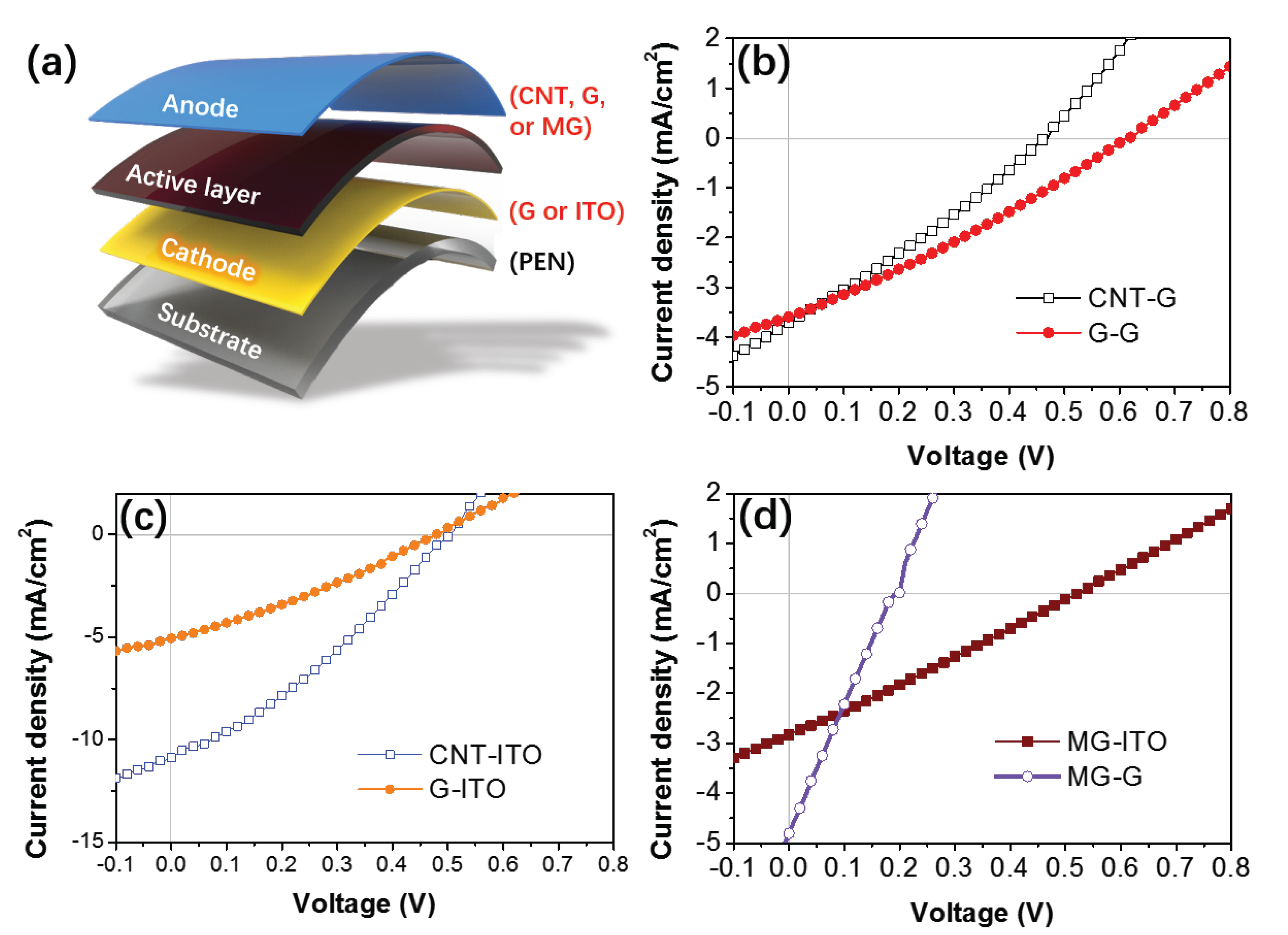
Using the abovementioned carbon-based films, we designed six pairs of carbon-based electrodes for OPV devices, including CNT films (G or MG films) as anodes and G films (or ITO) as cathodes (the corresponding devices are labeled as CNT-G, G-G, MG-G, CNT-ITO, G-ITO, MG-ITO, respectively), as shown in Figure 4a. Current density-voltage (J–V) characteristics of the OPVs with all-carbon electrodes and control devices with ITO-carbon electrodes are shown in Figure 4b–d. The photovoltaic parameters of all kinds of devices are extracted and summarized in Table 1. Figure 4b shows that similar values for short-circuit current density (Jsc) were achieved for CNT-G and G-G, despite the much lower sheet resistance of CNT films compared to few-layer graphene films. The reason for this is that the relatively higher optical transmittance of graphene films offsets this deficiency in conductivity. However, the open-circuit voltage (Voc) of CNT-G (0.47 V) is lower than G-G (0.62 V), which can be ascribed to the inferior heterojunction induced by the increased surface roughness and inhomogeneous cover of CNT networks. The results are identified by the dark J–V curves shown in Figure S8. Compared to CNT-G, G-G exhibits a more pronounced diode behavior and negligible reverse leakage current, which indicates the smoother and better interface formed between G electrodes and the adjacent layer. The performance of control cells with one-sided carbon electrodes could be investigated to further examine the competence of carbon-based electrodes. Figure 4c shows that G-ITO has a similar Voc (~0.50 V) to that of CNT-ITO, but a lower Jsc, which suggests that the conductivity is more contributive than transparency for carbon-based films as top anodes, in accordance with the reported conclusion by Xia et al. [31]. Moreover, the overall performance of MG-G is decreased seriously due to the low transmittance and high roughness of MG films, which is further identified by the results of MG-ITO (Figure 4d).
Although the better conductivity of MG films makes the corresponding devices generate moderate or even higher Jsc, the lower Voc and fill factor (FF) illustrate the increased destruction of active layer and carrier recombination caused by the roughness of the thicker graphene films. The PCEs of all-carbon electrodes devices are approximately one-third or half of those of the controls assembled with ITO-carbon electrodes, as shown in Table 1, in addition to G-G and G-ITO couples. The better performance of the ITO control cells could be attributed to the low sheet resistance (~10 Ω/sq.) and smoother surfaces (ceramic nature), facilitating small series resistance and optimized interface, which ensure the reasonable values of Jsc and Voc. As for the G-G cell, its performance is close to that of its G-ITO counterpart, showing the great potential of graphene to substitute the traditional metal grid. Moreover, the current densities of devices with all-carbon electrodes are comparable to those of devices based on an organic active layer with electrodes made of carbon-based and standard materials [29,31,33,45,48,56]. These results suggest that all-carbon electrodes composed of CNT and graphene films could efficiently collect and transport charge carriers towards an external circuit. The best photovoltaic response for devices with all-carbon electrodes (G-G) displays a Jsc of 3.6 mA/cm2, a Voc of 0.62 V, and an FF of 0.28, with a consequent PCE of 0.63%. Although the overall efficiencies are not competitive with those of the ITO controls, they are comparable to the performance of OPVs using pristine CVD graphene films as anodes on a smoother rigid substrate (glass) [45]. Therefore, the above results supply feasible evidence for applying all-carbon electrodes in carbon-based solar cells. It is believed that these carbon-based electrodes can be further improved for potentially high-efficient, low-cost, and green all-carbon solar cells.
4. Conclusions
In summary, using large-area and high quality CNT and graphene films, we successfully fabricated flexible and semitransparent solar cells with all-carbon electrodes. The current densities of all devices with all-carbon electrodes, including CNT-G, G-G and MG-G, are comparable to those reported for carbon-based devices with conventional anodes (ITO) and cathodes (Ag or Al). The best performance achieved for the devices with all-carbon electrodes is 0.63%, comparable to the performance of OPVs using pristine CVD graphene films as anodes. There is great room for improvement in film hydrophilicity, smoothness, and conductivity to ultimately obtain higher efficiencies. This development demonstrates the potential of graphitic nanomaterials as all-carbon electrodes for future flexible carbon-based photovoltaics and other thin-film solar cells.
Supplementary Materials
The following are available online at https://www.mdpi.com/2076-3417/8/2/152/s1. Figure S1: TEM images of ZnO nanoparticles, Figure S2: Photographs of as-grown graphene, Figure S3: Optical images of as-grown graphene, Figure S4: SEM images of as-grown few-layer graphene, Figure S5: Raman spectrum and transmittance spectrum of multi-layer graphene, Figure S6: AFM topography images of few-layer graphene, Figure S7: AFM topography images of CNT films, Figure S8: Dark J–V characteristics of solar cells with CNT (or G) as anodes and G as cathodes.
Acknowledgments
We acknowledge the support from the 973 program of China (Nos. 2015CB932500, 2014CB932401), National Natural Science Foundation of China (Nos. 51372131, 51722207, and 51372133), Beijing Nova Program (No. Z161100004916099), and Tsinghua University Initiative Scientific Research Program (No. 20151080367). Z.Z. gratefully acknowledges the financial support from the National Natural Science Foundation of China (No. 11364043).
Author Contributions
Zexia Zhang and Yi Jia conceived and designed the experiments; Zexia Zhang performed the experiments; Zexia Zhang and Xin Gan analyzed the data; Hongwei Zhu, Ruitao Lv, and Feiyu Kang contributed reagents/materials/analysis tools; Zexia Zhang and Ruitao Lv wrote the paper.
Conflicts of Interest
The authors declare no conflict of interest.
References
- Kroto, H.W.; Heath, J.R.; Obrien, S.C.; Curl, R.F.; Smalley, R.E. C60: Buckminsterfullerene. Nature 1985, 318, 162–163. [Google Scholar] [CrossRef]
- Iijima, S. Helical microtubules of graphitic carbon. Nature 1991, 354, 56–58. [Google Scholar] [CrossRef]
- Novoselov, K.S.; Geim, A.K.; Morozov, S.V.; Jiang, D.; Zhang, Y.; Dubonos, S.V.; Grigorieva, I.V.; Firsov, A.A. Electric field effect in atomically thin carbon films. Science 2004, 306, 666–669. [Google Scholar] [CrossRef] [PubMed]
- Lu, R.; Christianson, C.; Weintrub, B.; Wu, J.Z. High photoresponse in hybrid graphene-carbon nanotube infrared detectors. ACS Appl. Mater. Interfaces 2013, 5, 11703–11707. [Google Scholar] [CrossRef] [PubMed]
- Xie, Y.; Gong, M.; Shastry, T.A.; Lohrman, J.; Hersam, M.C.; Ren, S. Broad-spectral-response nanocarbon bulk-heterojunction excitonic photodetectors. Adv. Mater. 2013, 25, 3433–3437. [Google Scholar] [CrossRef] [PubMed]
- Bernardi, M.; Lohrman, J.; Kumar, P.V.; Kirkeminde, A.; Ferralis, N.; Grossman, J.C.; Ren, S. Nanocarbon-based photovoltaics. ACS Nano 2012, 6, 8896–8903. [Google Scholar] [CrossRef] [PubMed]
- Cai, X.; Hou, S.; Wu, H.; Lv, Z.; Fu, Y.; Wang, D.; Zhang, C.; Kafafy, H.; Chu, Z.; Zou, D. All-carbon electrode-based fiber-shaped dye-sensitized solar cells. Phys. Chem. Chem. Phys. 2012, 14, 125–130. [Google Scholar] [CrossRef] [PubMed]
- Chen, L.J.; Song, Q.L.; Xiong, Z.H.; Huang, J.H.; He, F. Environment-friendly energy from all-carbon solar cells based on fullerene-C60. Sol. Energy Mater. Sol. Cells 2011, 95, 1138–1140. [Google Scholar] [CrossRef]
- D’Souza, F.; Ito, O. Photosensitized electron transfer processes of nanocarbons applicable to solar cells. Chem. Soc. Rev. 2012, 41, 86–96. [Google Scholar] [CrossRef] [PubMed]
- Jain, R.M.; Howden, R.; Tvrdy, K.; Shimizu, S.; Hilmer, A.J.; McNicholas, T.P.; Gleason, K.K.; Strano, M.S. Polymer-free near-infrared photovoltaics with single chirality (6,5) semiconducting carbon nanotube active layers. Adv. Mater. 2012, 24, 4436–4439. [Google Scholar] [CrossRef] [PubMed]
- Tu, K.-H.; Li, S.-S.; Li, W.-C.; Wang, D.-Y.; Yang, J.-R.; Chen, C.-W. Solution processable nanocarbon platform for polymer solar cells. Energy Environ. Sci. 2011, 4, 3521–3526. [Google Scholar] [CrossRef]
- Tung, V.C.; Huang, J.H.; Tevis, I.; Kim, F.; Kim, J.; Chu, C.W.; Stupp, S.I.; Huang, J. Surfactant-free water-processable photoconductive all-carbon composite. J. Am. Chem. Soc. 2011, 133, 4940–4947. [Google Scholar] [CrossRef] [PubMed]
- Ramuz, M.P.; Vosgueritchian, M.; Wei, P.; Wang, C.; Gao, Y.; Wu, Y.; Chen, Y.; Bao, Z. Evaluation of solution-processable carbon-based electrodes for all-carbon solar cells. ACS Nano 2012, 6, 10384–10395. [Google Scholar] [CrossRef] [PubMed]
- Tung, V.C.; Huang, J.-H.; Kim, J.; Smith, A.J.; Chu, C.-W.; Huang, J. Towards solution processed all-carbon solar cells: A perspective. Energy Environ. Sci. 2012, 5, 7810–7818. [Google Scholar] [CrossRef]
- Bindl, D.J.; Wu, M.Y.; Prehn, F.C.; Arnold, M.S. Efficiently harvesting excitons from electronic type-controlled semiconducting carbon nanotube films. Nano Lett. 2011, 11, 455–460. [Google Scholar] [CrossRef] [PubMed]
- Bindl, D.J.; Safron, N.S.; Arnold, M.S. Dissociating excitons photogenerated in semiconducting carbon nanotubes at polymeric photovoltaic heterojunction interfaces. ACS Nano 2010, 4, 5657–5664. [Google Scholar] [CrossRef] [PubMed]
- Dabera, G.D.M.R.; Jayawardena, K.D.G.I.; Prabhath, M.R.R.; Yahya, I.; Tan, Y.Y.; Nismy, N.A.; Shiozawa, H.; Sauer, M.; Ruiz-Soria, G.; Ayala, P. Hybrid carbon nanotube networks as efficient hole extraction layers for organic photovoltaics. ACS Nano 2013, 7, 556–565. [Google Scholar] [CrossRef] [PubMed]
- Li, M.; Ni, W.; Kan, B.; Wan, X.; Zhang, L.; Zhang, Q.; Long, G.; Zuo, Y.; Chen, Y. Graphene quantum dots as the hole transport layer material for high-performance organic solar cells. Phys. Chem. Chem. Phys. 2013, 15, 18973–18978. [Google Scholar] [CrossRef] [PubMed]
- Qu, S.; Li, M.; Xie, L.; Huang, X.; Yang, J.; Wang, N.; Yang, S. Noncovalent functionalization of graphene attaching [6,6]-phenyl-c61-butyric acid methyl ester (pcbm) and application as electron extraction layer of polymer solar cells. ACS Nano 2013, 7, 4070–4081. [Google Scholar] [CrossRef] [PubMed]
- Yang, N.; Zhai, J.; Wang, D.; Chen, Y.; Jiang, L. Two-dimensional graphene bridges enhanced photoinduced charge transport in dye-sensitized solar cells. ACS Nano 2010, 4, 887–894. [Google Scholar] [CrossRef] [PubMed]
- Fang, Z.; Ito, A.; Stuart, A.C.; Luo, H.; Chen, Z.; Vinodgopal, K.; You, W.; Meyer, T.J.; Taylor, D.K. Soluble reduced graphene oxide sheets grafted with polypyridylruthenium-derivatized polystyrene brushes as light harvesting antenna for photovoltaic applications. ACS Nano 2013, 7, 7992–8002. [Google Scholar] [CrossRef] [PubMed]
- Lu, L.; Xu, T.; Chen, W.; Lee, J.M.; Luo, Z.; Jung, I.H.; Park, H.I.; Kim, S.O.; Yu, L. The role of n-doped multiwall carbon nanotubes in achieving highly efficient polymer bulk heterojunction solar cells. Nano Lett. 2013, 13, 2365–2369. [Google Scholar] [CrossRef] [PubMed]
- Ren, S.; Bernardi, M.; Lunt, R.R.; Bulovic, V.; Grossman, J.C.; Gradecak, S. Toward efficient carbon nanotube/P3HT solar cells: Active layer morphology, electrical, and optical properties. Nano Lett. 2011, 11, 5316–5321. [Google Scholar] [CrossRef] [PubMed]
- Wang, Y.; Tong, S.W.; Xu, X.F.; Ozyilmaz, B.; Loh, K.P. Interface engineering of layer-by-layer stacked graphene anodes for high-performance organic solar cells. Adv. Mater. 2011, 23, 1514–1518. [Google Scholar] [CrossRef] [PubMed]
- Hsu, C.L.; Lin, C.T.; Huang, J.H.; Chu, C.W.; Wei, K.H.; Li, L.J. Layer-by-layer graphene/TCNQ stacked films as conducting anodes for organic solar cells. ACS Nano 2012, 6, 5031–5039. [Google Scholar] [CrossRef] [PubMed]
- Liu, Z.K.; Li, J.H.; Sun, Z.H.; Tai, G.A.; Lau, S.P.; Yan, F. The application of highly doped single-layer graphene as the top electrodes of semitransparent organic solar cells. ACS Nano 2012, 6, 810–818. [Google Scholar] [CrossRef] [PubMed]
- Zhang, D.; Xie, F.X.; Lin, P.; Choy, W.C.H. Al-TiO2 composite-modified single-layer graphene as an efficient transparent cathode for organic solar cells. ACS Nano 2013, 7, 1740–1747. [Google Scholar] [CrossRef] [PubMed]
- Liu, Z.; Li, J.; Yan, F. Package-free flexible organic solar cells with graphene top electrodes. Adv. Mater. 2013, 25, 4296–4301. [Google Scholar] [CrossRef] [PubMed]
- Salvatierra, R.V.; Cava, C.E.; Roman, L.S.; Zarbin, A.J.G. Ito-free and flexible organic photovoltaic device based on high transparent and conductive polyaniline/carbon nanotube thin films. Adv. Funct. Mater. 2013, 23, 1490–1499. [Google Scholar] [CrossRef]
- Li, X.; Zhu, H.; Wang, K.; Cao, A.; Wei, J.; Li, C.; Jia, Y.; Li, Z.; Li, X.; Wu, D. Graphene-on-silicon schottky junction solar cells. Adv. Mater. 2010, 22, 2743–2748. [Google Scholar] [CrossRef] [PubMed]
- Xia, X.; Wang, S.; Jia, Y.; Bian, Z.; Wu, D.; Zhang, L.; Cao, A.; Huang, C. Infrared-transparent polymer solar cells. J. Mater. Chem. 2010, 20, 8478–8482. [Google Scholar] [CrossRef]
- Park, H.; Brown, P.R.; Bulovic, V.; Kong, J. Graphene as transparent conducting electrodes in organic photovoltaics: Studies in graphene morphology, hole transporting layers, and counter electrodes. Nano Lett. 2012, 12, 133–140. [Google Scholar] [CrossRef] [PubMed]
- Yin, Z.Y.; Sun, S.Y.; Salim, T.; Wu, S.X.; Huang, X.A.; He, Q.Y.; Lam, Y.M.; Zhang, H. Organic photovoltaic devices using highly flexible reduced graphene oxide films as transparent electrodes. ACS Nano 2010, 4, 5263–5268. [Google Scholar] [CrossRef] [PubMed]
- Wei, J.; Jia, Y.; Shu, Q.; Gu, Z.; Wang, K.; Zhuang, D.; Zhang, G.; Wang, Z.; Luo, J.; Cao, A. Double-walled carbon nanotube solar cells. Nano Lett. 2007, 7, 2317–2321. [Google Scholar] [CrossRef] [PubMed]
- Park, H.; Chang, S.; Zhou, X.; Kong, J.; Palacios, T.; Gradecak, S. Flexible graphene electrode-based organic photovoltaics with record-high efficiency. Nano Lett. 2014, 14, 5148–5154. [Google Scholar] [CrossRef] [PubMed]
- Jia, Y.; Wei, J.; Wang, K.; Cao, A.; Shu, Q.; Gui, X.; Zhu, Y.; Zhuang, D.; Zhang, G.; Ma, B. Nanotube-silicon heterojunction solar cells. Adv. Mater. 2008, 20, 4594–4598. [Google Scholar] [CrossRef]
- Liu, Z.; You, P.; Liu, S.; Yan, F. Neutral-color semitransparent organic solar cells with all-graphene electrodes. ACS Nano 2015, 9, 12026–12034. [Google Scholar] [CrossRef] [PubMed]
- Song, Y.; Chang, S.; Gradecak, S.; Kong, J. Visibly-transparent organic solar cells on flexible substrates with all-graphene electrodes. Adv. Energy Mater. 2016, 6, 1600847. [Google Scholar] [CrossRef]
- Dang, M.T.; Hirsch, L.; Wantz, G. P3HT:PCBM, best seller in polymer photovoltaic research. Adv. Mater. 2011, 23, 3597–3602. [Google Scholar] [CrossRef] [PubMed]
- Yu, G.; Gao, J.; Hummelen, J.C.; Wudl, F.; Heeger, A.J. Polymer photovoltaic cells: Enhanced efficiencies via a network of internal donor-acceptor heterojunctions. Science 1995, 270, 1789–1791. [Google Scholar] [CrossRef]
- Chen, C.C.; Dou, L.; Zhu, R.; Chung, C.H.; Song, T.B.; Zheng, Y.B.; Hawks, S.; Li, G.; Weiss, P.S.; Yang, Y. Visibly transparent polymer solar cells produced by solution processing. ACS Nano 2012, 6, 7185–7190. [Google Scholar] [CrossRef] [PubMed]
- Rowell, M.W.; Topinka, M.A.; McGehee, M.D.; Prall, H.-J.; Dennler, G.; Sariciftci, N.S.; Hu, L.; Gruner, G. Organic solar cells with carbon nanotube network electrodes. Appl. Phys. Lett. 2006, 88, 233506. [Google Scholar] [CrossRef]
- Liu, D.; Zhao, M.; Li, Y.; Bian, Z.; Zhang, L.; Shang, Y.; Xia, X.; Zhang, S.; Yun, D.; Liu, Z. Solid-state, polymer-based fiber solar cells with carbon nanotube electrodes. ACS Nano 2012, 6, 11027–11034. [Google Scholar] [CrossRef] [PubMed]
- Cho, D.-Y.; Eun, K.; Choa, S.-H.; Kim, H.-K. Highly flexible and stretchable carbon nanotube network electrodes prepared by simple brush painting for cost-effective flexible organic solar cells. Carbon 2014, 66, 530–538. [Google Scholar] [CrossRef]
- Wang, Y.; Chen, X.; Zhong, Y.; Zhu, F.; Loh, K.P. Large area, continuous, few-layered graphene as anodes in organic photovoltaic devices. Appl. Phys. Lett. 2009, 95, 063302. [Google Scholar] [CrossRef]
- Xu, Y.; Long, G.; Huang, L.; Huang, Y.; Wan, X.; Ma, Y.; Chen, Y. Polymer photovoltaic devices with transparent graphene electrodes produced by spin-casting. Carbon 2010, 48, 3308–3311. [Google Scholar] [CrossRef]
- Petridis, C.; Konios, D.; Stylianakis, M.M.; Kakavelakis, G.; Sygletou, M.; Savva, K.; Tzourmpakis, P.; Krassas, M.; Vaenas, N.; Stratakis, E. Solution processed reduced graphene oxide electrodes for organic photovoltaics. Nanoscale Horiz. 2016, 1, 375–382. [Google Scholar] [CrossRef]
- Lee, Y.Y.; Tu, K.H.; Yu, C.C.; Li, S.S.; Hwang, J.Y.; Lin, C.C.; Chen, K.H.; Chen, L.C.; Chen, H.L.; Chen, C.W. Top laminated graphene electrode in a semitransparent polymer solar cell by simultaneous thermal annealing/releasing method. ACS Nano 2011, 5, 6564–6570. [Google Scholar] [CrossRef] [PubMed]
- Hecht, D.S.; Hu, L.; Irvin, G. Emerging transparent electrodes based on thin films of carbon nanotubes, graphene, and metallic nanostructures. Adv. Mater. 2011, 23, 1482–1513. [Google Scholar] [CrossRef] [PubMed]
- Lee, S.K.; Rana, K.; Ahn, J.H. Graphene films for flexible organic and energy storage devices. J. Phys. Chem. Lett. 2013, 4, 831–841. [Google Scholar] [CrossRef] [PubMed]
- Hau, S.K.; Yip, H.-L.; Baek, N.S.; Zou, J.; O’Malley, K.; Jen, A.K.Y. Air-stable inverted flexible polymer solar cells using zinc oxide nanoparticles as an electron selective layer. Appl. Phys. Lett. 2008, 92, 253301. [Google Scholar] [CrossRef]
- Lin, Y.; Li, X.; Xie, D.; Feng, T.; Chen, Y.; Song, R.; Tian, H.; Ren, T.; Zhong, M.; Wang, K. Graphene/semiconductor heterojunction solar cells with modulated antireflection and graphene work function. Energy Environ. Sci. 2013, 6, 108–115. [Google Scholar] [CrossRef]
- Bianco, A.; Cheng, H.-M.; Enoki, T.; Gogotsi, Y.; Hurt, R.H.; Koratkar, N.; Kyotani, T.; Monthioux, M.; Park, C.R.; Tascon, J.M.D. All in the graphene family: A recommended nomenclature for two-dimensional carbon materials. Carbon 2013, 65, 1–6. [Google Scholar] [CrossRef]
- Ferrari, A.C.; Meyer, J.C.; Scardaci, V.; Casiraghi, C.; Lazzeri, M.; Mauri, F.; Piscanec, S.; Jiang, D.; Novoselov, K.S.; Roth, S. Raman spectrum of graphene and graphene layers. Phys. Rev. Lett. 2006, 97, 187401. [Google Scholar] [CrossRef] [PubMed]
- Nair, R.R.; Blake, P.; Grigorenko, A.N.; Novoselov, K.S.; Booth, T.J.; Stauber, T.; Peres, N.M.; Geim, A.K. Fine structure constant defines visual transparency of graphene. Science 2008, 320, 1308. [Google Scholar] [CrossRef] [PubMed]
- Gomez De Arco, L.; Zhang, Y.; Schlenker, C.W.; Ryu, K.; Thompson, M.E.; Zhou, C. Continuous, highly flexible, and transparent graphene films by chemical vapor deposition for organic photovoltaics. ACS Nano 2010, 4, 2865–2873. [Google Scholar] [CrossRef] [PubMed]
Figure 1.
(a) Schematic illustration and (b) energy level diagram of the solar cells fabricated with carbon nanotube (CNT) or graphene (G) films as anodes and graphene film as cathode. PEDOT:PSS denotes poly(3,4-ethylenedioxythiophene):poly(styrenesulfonate). P3HT and PCBM denote poly(3-hexyl)thiophene and phenyl-C61-butyricacid methyl ester, respectively; (c) Photograph of a semitransparent solar cell with all-carbon electrodes; (d) Good flexibility of as-obtained solar cell device.
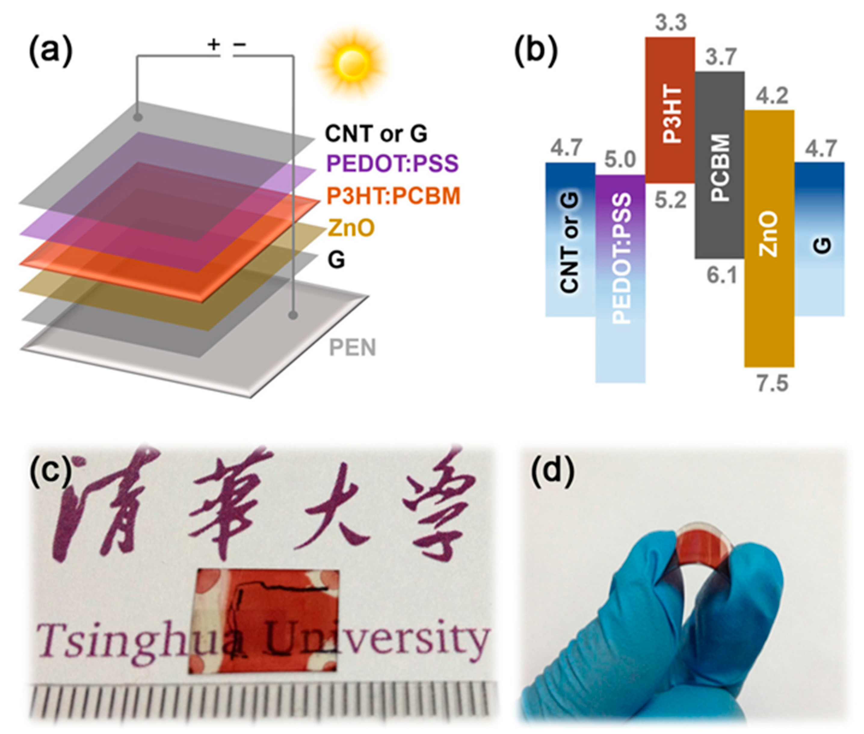
Figure 2.
(a) Photograph of a few-layer graphene film transferred onto a polyethylene naphthalate (PEN) substrate; (b) High-resolution transmission electron microscopy (TEM) image of as-synthesized few-layer graphene film. Inset shows the corresponding selected area electron diffraction (SAED) pattern; (c) Raman spectrum and (d) transmittance spectrum of the as-synthesized few-layer graphene film.
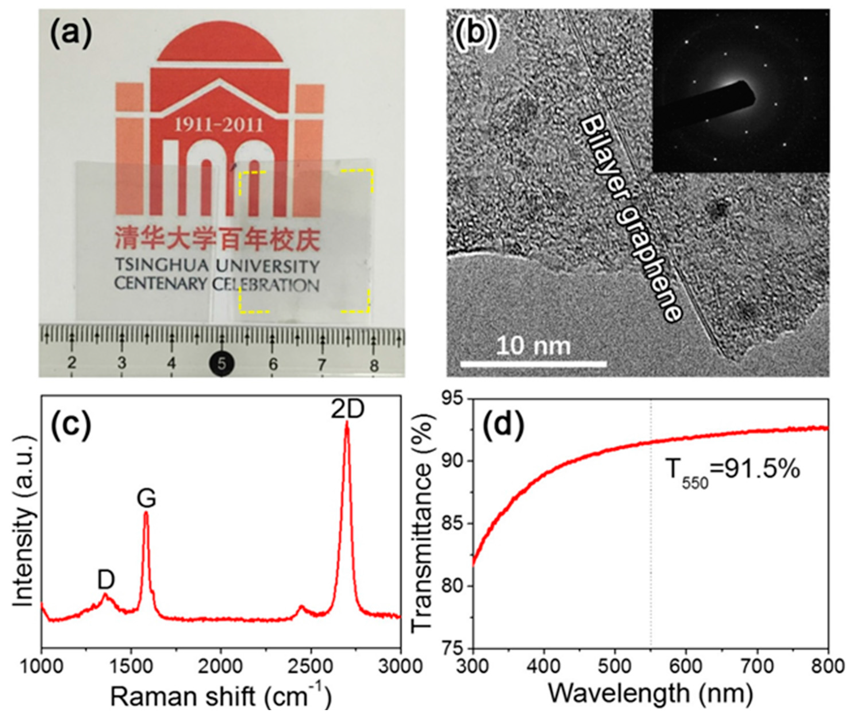
Figure 3.
Photographs of (a) the as-grown CNT film on nickel foil and (b) the CNT film transferred onto a PEN substrate; (c) scanning electron microscopy (SEM) and (d) TEM images of the as-synthesized CNT film; (e) Raman spectrum and (f) visible transmittance spectrum of the as-synthesized CNT film.
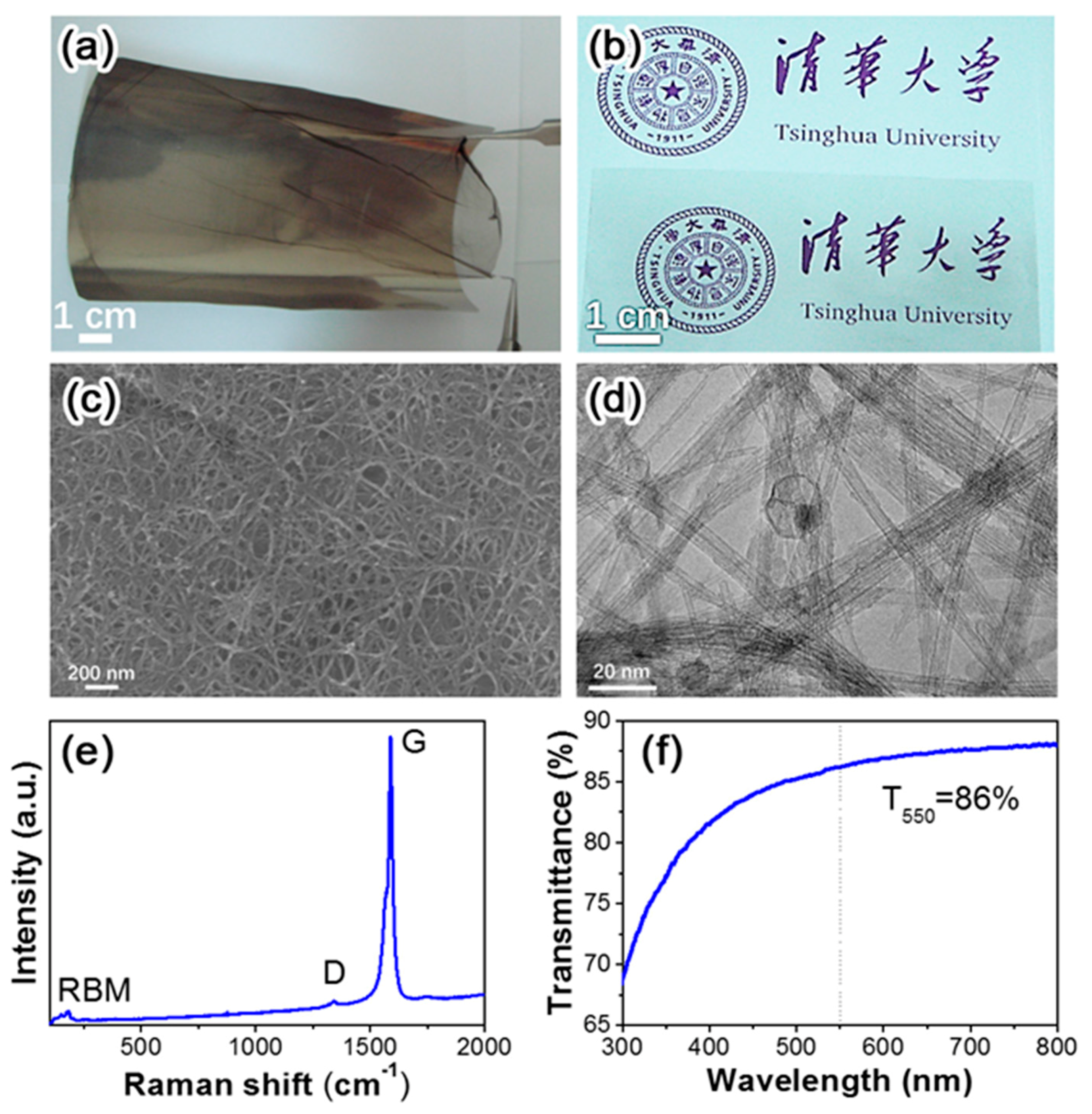
Figure 4.
(a) Schematic illustration of flexible solar cell devices with all-carbon electrodes and their indium tin oxide (ITO) analogues; (b) J–V characteristics of solar cells with CNT (or G) as the anode and G as the cathode; (c) J–V characteristics of control devices using ITO as the cathode and CNT (or G) as the anode; (d) J–V characteristics of solar cells with MG as the anode and G (or ITO) as the cathode. Here “G” and “MG” denote few-layer graphene films and multi-layer graphene films, respectively.

Table 1.
Photovoltaic parameters of different solar cell devices.
| Samples | Voc (V) | Jsc (mA/cm2) | FF (%) | η (%) |
|---|---|---|---|---|
| CNT-G | 0.47 | 3.7 | 28 | 0.48 |
| CNT-ITO | 0.50 | 10.9 | 32 | 1.71 |
| G-G | 0.62 | 3.6 | 28 | 0.63 |
| G-ITO | 0.48 | 5.1 | 30 | 0.73 |
| MG-G | 0.20 | 4.8 | 23 | 0.22 |
| MG-ITO | 0.50 | 3.6 | 29 | 0.50 |
© 2018 by the authors. Licensee MDPI, Basel, Switzerland. This article is an open access article distributed under the terms and conditions of the Creative Commons Attribution (CC BY) license (http://creativecommons.org/licenses/by/4.0/).
Share and Cite
MDPI and ACS Style
Zhang, Z.; Lv, R.; Jia, Y.; Gan, X.; Zhu, H.; Kang, F. All-Carbon Electrodes for Flexible Solar Cells. Appl. Sci. 2018, 8, 152. https://doi.org/10.3390/app8020152
AMA Style
Zhang Z, Lv R, Jia Y, Gan X, Zhu H, Kang F. All-Carbon Electrodes for Flexible Solar Cells. Applied Sciences. 2018; 8(2):152. https://doi.org/10.3390/app8020152
Chicago/Turabian StyleZhang, Zexia, Ruitao Lv, Yi Jia, Xin Gan, Hongwei Zhu, and Feiyu Kang. 2018. "All-Carbon Electrodes for Flexible Solar Cells" Applied Sciences 8, no. 2: 152. https://doi.org/10.3390/app8020152
Note that from the first issue of 2016, this journal uses article numbers instead of page numbers. See further details here.