Article

Influence of Substrate Stage Temperature and Rotation Rate on the Magneto-Optical Quality of RF-Sputtered Bi2.1Dy0.9Fe3.9Ga1.1O12 Garnet Thin Films

Electron Science Research Institute, Edith Cowan University, 270 Joondalup Drive, Joondalup, WA 6027, Australia
*
Author to whom correspondence should be addressed.
Appl. Sci. 2018, 8(3), 456; https://doi.org/10.3390/app8030456
Submission received: 18 January 2016 / Revised: 7 March 2018 / Accepted: 13 March 2018 / Published: 16 March 2018
(This article belongs to the Section Materials Science and Engineering)

Abstract

:
Highly bismuth-substituted iron garnet thin films are prepared on quartz substrates by using a radio frequency (RF) magnetron sputtering technique. We study the factors (process parameters associated with the RF magnetron sputter deposition technique) affecting the magneto-optical (MO) properties of ferrite garnet films of composition Bi2.1Dy0.9Fe3.9Ga1.1O12. All films show high MO response across the visible range of wavelengths after being annealed. In particular, the effects of substrate stage temperature and rotation rate on the various properties of films are studied. Experimental results reveal that the characteristics of garnet films of this type can be tuned and optimized for use in various magnetic field-driven nanophotonics and integrated optics devices, and that, at a substrate stage rotation rate near 16 revolutions per minute, the MO quality of the developed MO films is the best, in comparison with films deposited at other rotation rates. To the best of our knowledge, this is the first report on the effects of deposition parameters on the properties of garnet films of this stoichiometry.

1. Introduction

Bismuth (Bi)-substituted magneto-optical (MO) garnet materials are very attractive for use in various technological applications such as magnetic memory, magnetoplasmonic devices, magneto-optic sensors, lightwave polarization controllers, and MO spatial or temporal light modulators [1,2,3,4,5,6,7,8,9,10,11]. They possess record-high Faraday or Kerr effects simultaneously with low optical losses in parts of the visible and near-infrared regions and are starting to become highly sought after for the development of cost-effective and reliable photonic devices and sensors. Since the 1960s, Bi-substituted MO garnet thin films have been fabricated with different compositional stoichiometries using deposition technologies such as Pulsed Laser Deposition (PLD), Liquid-Phase Epitaxy (LPE), Ion Beam Sputtering (IBS), Reactive Ion Beam Sputtering (RIBS), metal–organic chemical vapor deposition (MOCVD), sol-gel technique, and radio frequency (RF) magnetron sputtering, and using other material synthesis systems [5,12,13,14,15,16,17,18,19]. All of these physical vapor deposition techniques require complex and multiparameter process optimizations at both the deposition and annealing (crystallization) stages. RF magnetron sputtering deposition followed by a high-temperature oven crystallization process is one of the most flexible and compatible approaches to synthesizing MO garnet materials. However, there are multiple important process-related factors associated with the preparation of MO garnet thin films that affect their properties and quality. Many of these factors are related to the parameters of the magnetron sputter deposition technique used to fabricate garnet films, such as the substrate type, the substrate temperature, the substrate stage rotation rate, and the deposition environment (process gas(es) and their partial pressure(s)), and need to be controlled carefully to optimize the film properties. Other factors defining the properties of garnet film layers are associated with the annealing process. In the past, several studies have been conducted to investigate the effects of process parameters on the optical and magneto-optical properties of garnet films [20,21,22]. It has been reported that the variations of deposition process parameters such as the substrate stage temperature, target rotation frequencies, argon pressure, and RF power densities applied to the sputtering target all affect the properties of garnet thin films through inducing changes in the film morphology and density [21,22,23,24,25,26,27]. Also, the annealing heat treatment regime can affect the optical and MO properties through the crystallization process kinetics by changing the microstructure and crystallite sizes of garnet layers [28].
In this paper, we investigate the effects of process parameters—in particular, the substrate stage temperature and substrate stage rotation rate—associated with the RF sputter deposition technique, on the properties (stoichiometry, optical, and magneto-optical parameters) of garnet thin films sputtered in a pure argon atmosphere from an oxide-mix-based ceramic target material of composition type Bi2.1Dy0.9Fe3.9Ga1.1O12.

2. Materials and Methods

Several batches of highly bismuth-substituted iron garnet films were sputtered on 0.5 mm thick quartz substrates from an oxide-mix-based target of nominal composition Bi2.1Dy0.9Fe3.9Ga1.1O12 with some variations in their deposition process parameters (using different substrate temperatures and substrate stage rotation rates). This target was prepared by the manufacturer (AJA Inc., Scituate, MA, USA) by sintering a stoichiometrically adjusted mix of oxides such as Bi2O3, Dy2O3, Fe2O3, and Ga2O3. As the sputter gas pressure during the layer growth typically does affect the film’s microstructure and properties (according to our previous garnet microstructure observations, measurements of the film’s refractive index, and the measurements of specific Faraday rotation), the sputtering process gas chemistry (Ar) and pressure were kept constant (at 2 mTorr) for all batches of samples. During the sputtering processes, RF powers of up to 175 W (3.8 W/cm2) were applied to ablate targets 7.62 cm. (3 in.) in diameter. The sputtering deposition system (KVS-T4065, from Korea Vacuum Technology Ltd., Gyeonggi-do, \Korea) was of the down-sputtering type. Its geometric features allowed high-uniformity deposition over a substrate holder area of about 5 cm in diameter, owing to the relatively large substrate-to-target distance of 18 cm. In the vertical plane cross section, the directions normal to the sputtering target surfaces form 30° angles with the normal to the (horizontal) substrate stage surface. In the horizontal plane cross section passing through the target centers, the target centers are positioned at the vertices of an equilateral triangle having side dimension of about 150 mm.
The optimizations of high-temperature annealing process parameters were performed by running several trials of both the deposition and annealing processes, followed by the selection of parameters, which led to maximizing specific Faraday rotation in films of good optical quality. The effects of variation in the substrate temperature and substrate stage rotation rate used during the deposition process on the final properties of material were first assessed by analyzing the obtained specific Faraday rotations at 532 nm and also the MO figures of merit. The presence of high specific Faraday rotations observed in these highly Bi-substituted garnet layers confirmed the formation of crystalline garnet phase, which was also reconfirmed by performing the X-ray diffractometry (XRD) measurements. The physical thicknesses of all garnet layers were measured directly during the deposition processes using a quartz microbalance sensor, and were also reconfirmed by spectrally fitting the transmission spectra of all films to their predicted transmission spectra using specialized software tools [5]. The software-assisted indirect film thickness measurements also allowed detection of any differences in the layer thickness values for the different samples from within the same deposition batch, which could arise due to the slight nonuniformities in the deposited thickness.
The optical transmission spectra of both the as-deposited and post-annealed garnet films were measured using a UV–Visible spectrophotometer (Beckman Coulter Inc., Atlanta, GA, USA) and the specific Faraday rotation of annealed garnet layers was measured using a Thorlabs PAX polarimeter system (Thorlabs Inc, Newton, NJ, USA) in conjunction with a custom-made calibrated electromagnet. XRD measurements were performed by using Cu Kα1 radiation line in theta–theta diffractometer configuration, at near-grazing incidence of X-ray radiation. The measurements were performed using a diffracted beam collimator with 2θ in the range of 20° to 70°. The angular positions of the X-ray diffraction peaks were determined by using the peak-listing options of the Jade ver. 9.0 (MDI Corp., Livermore, CA, USA) software package. The data obtained from the annealed samples showed X-ray diffraction peaks at the sets of angles characteristic of the body-centered cubic lattice structure of garnets, and revealed their crystalline microstructure. The average lattice constant and the crystallite size of the garnet films were calculated using identifiable diffraction lines and the standard methods explained in refs [29,30,31]. In this series of Bi2.1Dy0.9Fe3.9Ga1.1O12 samples (prepared on quartz substrates using the above-mentioned process parameter variation types) the averaged XRD-derived lattice constant was close to 12.52 (±0.05) Å, and the theory-calculated [29] lattice constant corresponding to the garnet of nominal stoichiometry identical to that of the sputtering target was 12.53 Å. To determine the approximate elemental composition of these thin films, energy dispersive spectroscopy (EDS) microanalysis experiments were carried out using an EDS Quantax Q100 (Bruker Corp., Billerica, MA, USA) system installed in conjunction with a scanning electron microscope (SEM). The results of these measurements were affected by the additional oxygen content from air trapped within film pores, as well as by the (expected) bismuth loss occurring during the deposition processes. For each sample, the EDS measurements were performed multiple—at least four—times on different spots on the sample surface, to acquire the approximate compositional information. Figure 1 shows an example of typical data output obtained from an annealed Bi2.1Dy0.9Fe3.9Ga1.1O12 film layer. Based on the measured elemental concentration data (in atomic %), the approximate averaged bismuth content was derived considering possible experimental errors related to the presence of oxygen molecules trapped within the films’ pores and to detection of the reflection spectrum from the sample’s surface, generated by the X-rays incident on the sample.

3. Results and Discussion

The effects of the sputtering process parameters on garnet thin-film materials of composition type Bi2.1Dy0.9Fe3.9Ga1.1O12 were studied experimentally, by way of evaluating the microstructural, optical, and magneto-optical properties. The obtained results of the optical and MO characterization of garnet films revealed a combination of moderate optical absorption with good surface and MO quality.

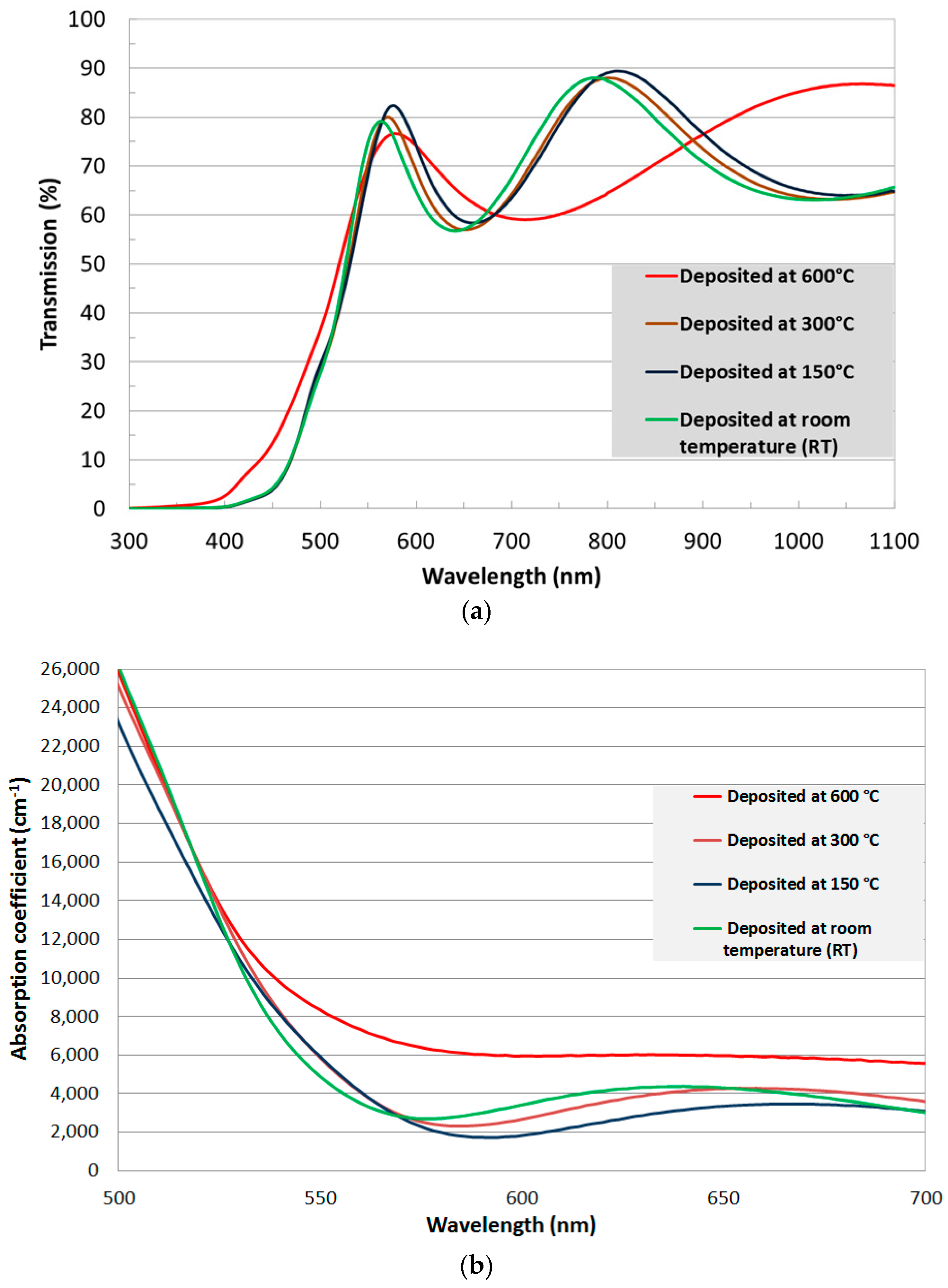
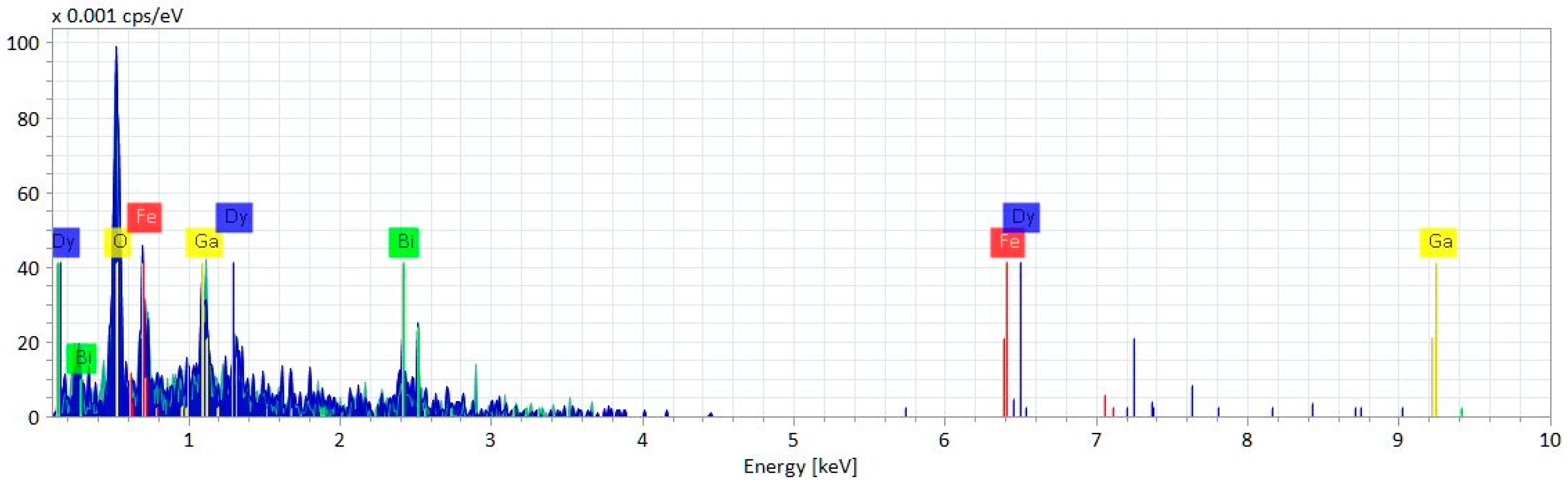
3.1. Substrate Temperature Effects

To investigate the effects of substrate temperature on the growth of this type of garnet film and on their optical and magneto-optical behaviors, we prepared four batches of samples, named ST1, ST2, ST3 and ST4, using significantly different substrate temperatures, from room temperature (RT) to 600 °C, but keeping all other deposition process parameters constant (including the deposition run time). The film thicknesses were monitored using a microbalance quartz sensor during the garnet layer deposition process and later remeasured based on the fitting of the measured and modelled transmission spectra using in-house developed and validated Magnetic Photonic Crystal (MPC) analysis software [5] as well as the commercially available OptiLayer software (http://www.optilayer.com). The as-deposited garnet layers (which were amorphous in phase) from each batch were annealed using the same crystallization process (at 670 °C for 1 h) by using a conventional air-atmosphere oven annealing heat treatment applied just after the deposition process. Note that, after annealing, it was also found that the thicknesses of the films closely matched those measured directly by the quartz sensor. The thickness errors were less than ±2%.
The bismuth content, as derived from the EDS datasets, within all deposited films in all experiments conducted at different substrate temperatures and rotation rates varied between 1.75 and 1.9 formula units. The specific Faraday rotation and the optical absorption coefficients at 532 nm were determined to calculate the MO figures of merit in Figure 2. After annealing, it was observed that the samples prepared on quartz substrates at room temperatures showed better MO properties (the highest Faraday rotation and MO figure of merit, as summarized in Table 1) at the 532 nm wavelength, though all of the annealed garnet films had relatively high absorption coefficients at 532 nm. It has also been noted that the absorption coefficient increased at very high substrate temperature (e.g., 600 °C) in Figure 2b, consequently reducing the MO quality (figure of merit) of the garnet layers. However, the films deposited at a higher temperature showed comparatively lower coercive force values. The lowest coercive force, of about 100 Oe, was measured for films deposited at 300 °C. The XRD datasets in Figure 2c obtained from the annealed garnet layers deposited at different substrate temperatures show sharp and well-defined diffraction peaks, indicating good crystallinity of the materials synthesized. In addition, it can be seen clearly that comparatively stronger diffraction peak intensities were observed in films deposited at room temperature, and the peak intensities tended to become weaker with increasing substrate temperature. The higher peak intensities may relate to obtaining increased volumetric fraction of the crystalline garnet phase present in these samples, which can also be related to higher MO performance observed in samples deposited at room temperature. The elemental composition data, represented as measured element concentrations in atomic %, collected from the as-deposited garnet films prepared at different substrate stage temperatures are summarized in Figure 2d. The Bi content, compared with the nominal stoichiometry of the sputtering target, was found to vary, owing to the varying loss of Bi atoms during the film growth process, in all garnet samples. The exact ratio between Fe and Ga contents in terms of atom numbers per formula unit (f.u.) was also found to be slightly different from the ratio estimated. A larger-than-expected (>60 atomic %) oxygen content measured in all films indicated some experimental errors originating from the oxygen atoms being either present within the substrate pores or trapped within the film pores. For the amorphous-phase garnet-type layer, deposited from a metal-oxide mixed sputtering target of nominal composition Bi2.1Dy0.9Fe3.9Ga1.1O12, only the volume-averaged composition of films could be derived (Table 1) from the obtained EDS data. The experimental results summarized in this section can be used as a guide for depositing new garnet-type thin-film materials with high MO performance.

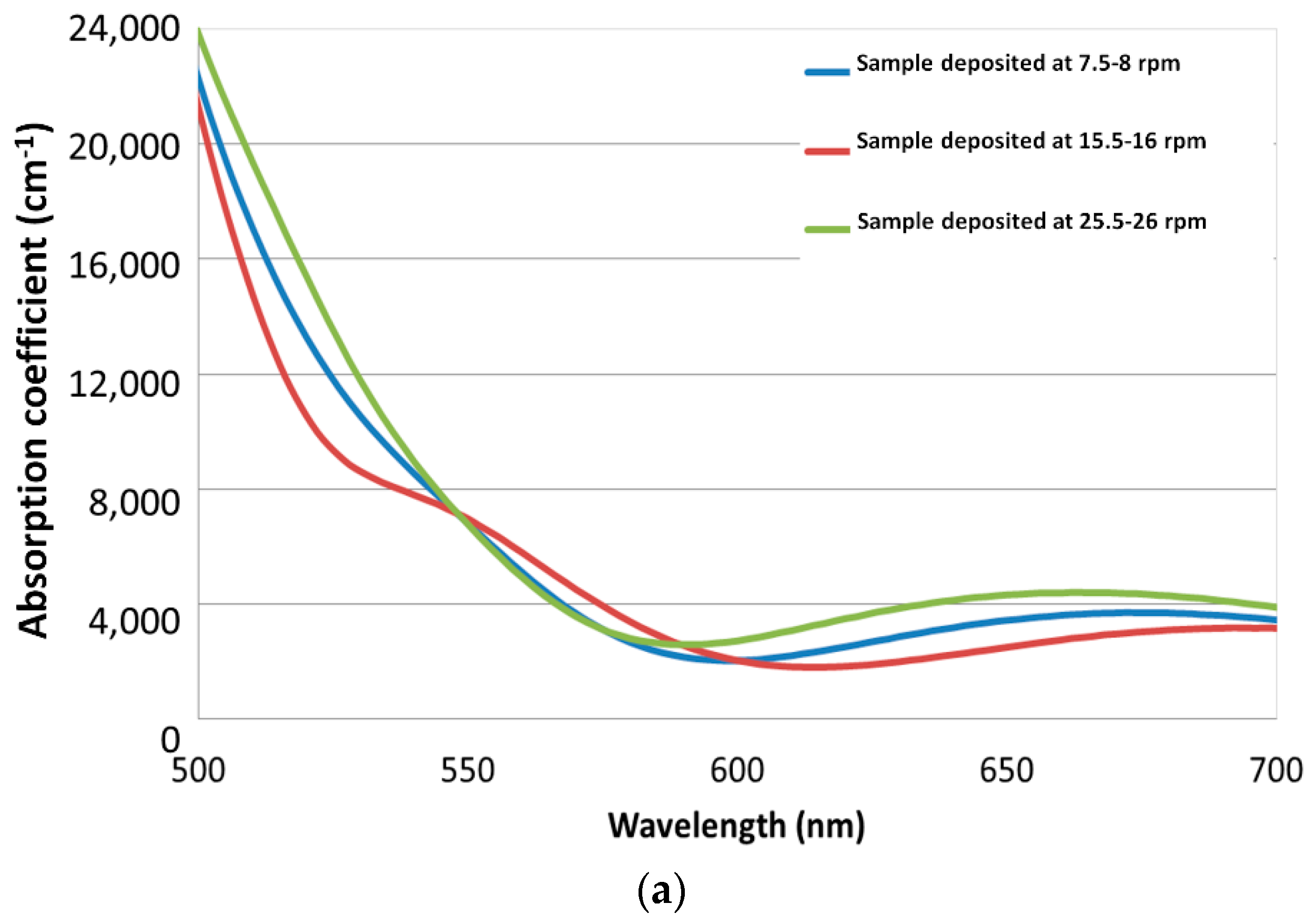
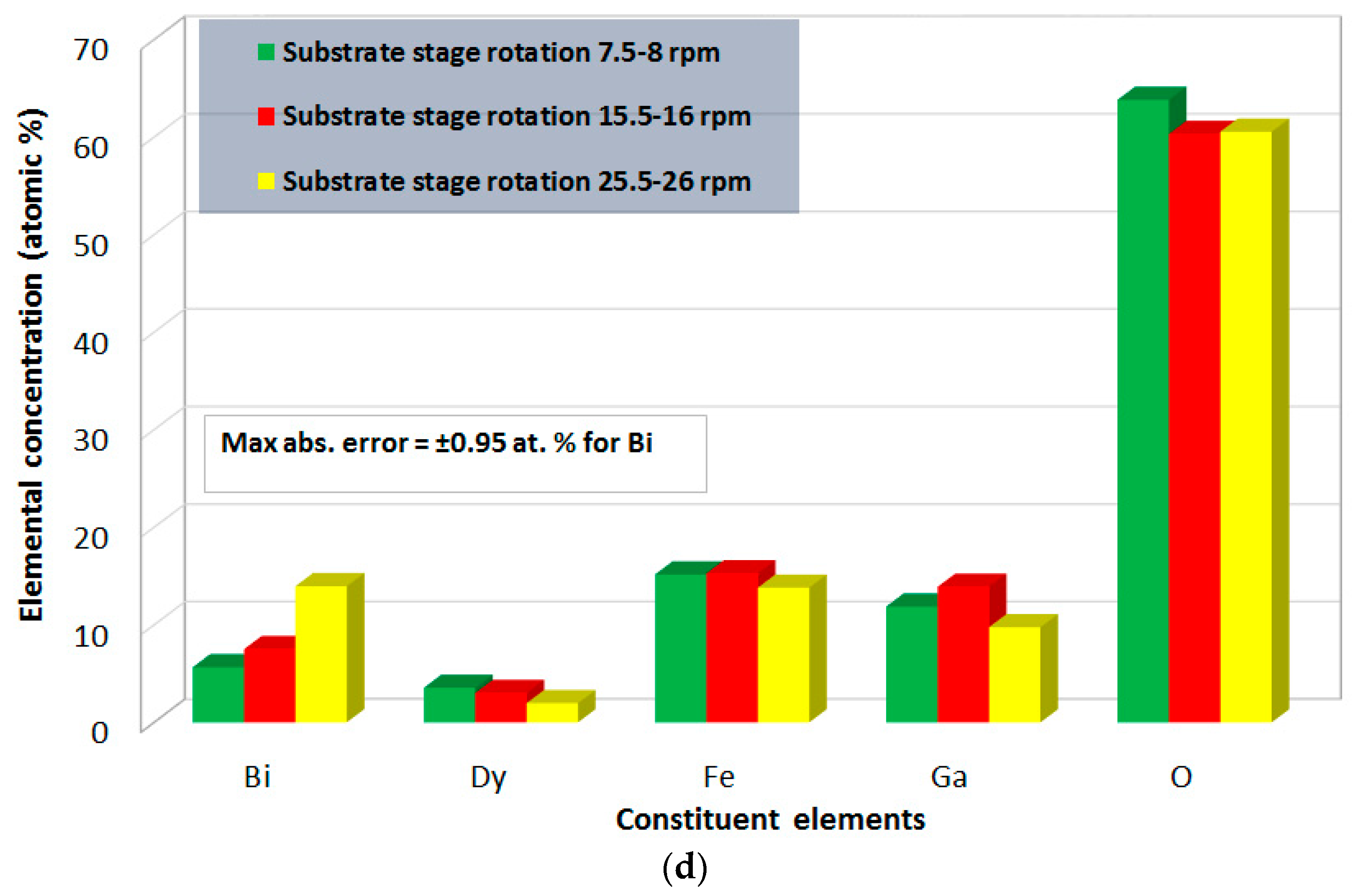
3.2. Substrate Stage Rotation Rate Effects

In order to investigate the somewhat unexpected effect of substrate stage rotation rate on the MO properties of this type of garnet materials, we deposited three batches of films (named SS1, SS2, and SS3) onto quartz substrates using three different substrate stage rotation rates (7.5–8, 15.5–16, 25.5–26 revolutions per minute (rpm)). Substrate stage rotation is widely used in most (or all) physical vapor deposition technologies and is known to improve the area uniformity of the deposited film thickness. Relatively few studies reported so far in the literature have concentrated on uncovering other effects of substrate rotation rate on the functional properties of thin films, e.g., [21,22]. Initially, we did not expect the MO quality factor in magnetic garnets to be significantly dependent on the substrate stage rotation rate; however, it was found that an optimum rotation rate existed, at least for this composition type. For each batch of samples, all other deposition process parameters were kept identical. All three batches of samples were annealed in one annealing run using the best-identified annealing regime for garnet films of this stoichiometry type (6 h at 580 °C or, alternatively, 1 h at 670 °C), which was found by running multiple annealing experiments. The optical absorption coefficients were software-fitted using spectrophotometry measurement results across the entire visible spectral range (Figure 3a). There were significant (and initially completely unexpected) differences observed in the MO properties of films fabricated at different substrate stage rotation rates (in terms of the MO figure of merit); a summary of measured properties is shown in Table 2.
The samples prepared using the 15.5–16 rpm substrate stage rotation rate repeatedly showed a better MO performance (in terms of the specific Faraday rotation and the MO figure of merit measured at 532 nm). These samples also had lower coercive force and saturation magnetization values compared with the films prepared using higher substrate stage rotation rates, as shown in Table 2. We repeated the deposition and annealing processes more than once, and again observed the same trends in the dependency of the MO properties on this process parameter.
Figure 3b shows the data on the substrate stage rotation-frequency-dependent evolution of the measured MO figure of merit obtained in Bi2.1Dy0.9Fe3.9Ga1.1O12 films prepared on quartz substrates. The data point distributions within the data clusters shown within the circles followed the observed trend of the MO quality factor for each of the annealing regimes used. Both of the annealing regimes (6 h at 580 °C and 1 h at 670 °C) had been previously established for this material type based on a large number of trials; each processing regime led to the best achievable results in terms of the optical and MO quality of films. The prominent peaks observed in the XRD patterns of samples SS1, SS2, and SS3 indicated that the garnet layers were grown homogeneously on the quartz substrates, even though there were some small differences in the peaks’ angular positions (Figure 3c). These differences may be related to the variations in the state of mechanical stress in films subjected to different thermal processing regimes, which could affect the lattice parameters. The intensity of diffraction peaks from the samples prepared using the 15.5–16 rpm stage rotation rate (SS2) was higher than that seen in samples SS1 and SS3, which implies that the volumetric contents of garnet phase within the films’ volume differed. The measured average crystallite size (derived using Scherrer’s formula) was in the range of 31–37 nm. The larger (average) crystallite size was observed (~36.8 nm) also in films prepared using the 15.5–16.0 rpm substrate stage rotation rate, compared to the films grown at either lower or higher substrate stage rotation rates. The values of average crystallite size are also listed in Table 2.
Using slower rotation rate helps to spontaneously grow porous films on the substrates and also increases the surface roughness, which affects the entropy of the garnet films and the MO performance [22], while the higher substrate stage rotation rates also contribute to the nucleation of pores in garnet layers. Increasing the surface roughness of the film reduces the garnet film quality in terms of the optical and MO properties. The EDS elemental compositional analysis also showed that the samples sputtered using the rotation rate of around 15.5–16.0 rpm had a slightly higher Bi content compared with other samples (Table 2). Figure 3d presents the measured elemental concentrations (in atomic %) obtained from the as-deposited films prepared using different substrate stage rotation rates.
The substrate stage rotation rate is one of the physical parameters affecting the initial stages of the thin film growth process, most likely by influencing the uniformity of adatom growth and nucleation across the substrate surface. This is because the time scale (of the order of 1 s) related to the formation of ultrathin (adatom-scale) initial film layers is, for the usual sputtering deposition rates of a few nanometers per minute, very similar to the periodicity of substrate stage rotation used in most deposition experiments. More studies are necessary to uncover the physical phenomena and processes linking the substrate stage rotation rate to the properties of ultrathin transitional layers forming near the film–substrate interface, including other process details, such as Thornton zone-based growth-model-related parameters [32,33]. The properties of transitional layers existing near the film–substrate interface represent a defining factor which governs the annealing crystallization process, since the crystallization processes initialize within this transitional region [2,34].

4. Conclusions

The variations in the magneto-optic properties of RF-sputtered thin garnet films of stoichiometry Bi2.1Dy0.9Fe3.9Ga1.1O12 occurring in response to varying deposition process parameters (substrate temperature and rotation rate) have been studied and reported for the first time. In particular, unexpected effects of varying the substrate rotation rate on the MO quality factor have been found, yet have been confirmed across multiple deposition batches. Experiments have demonstrated that the variations in RF sputtering process parameters have affected the garnet films’ stoichiometry and MO quality through variations in both the specific Faraday rotation and the optical absorption coefficients. We found that an optimum substrate stage rotation rate existed at near 16 revolutions per minute for our deposition system, leading to consistently obtaining ferrite garnet films of improved MO quality (up to 15.1° at 532 nm) compared with films grown at slower or faster rotation rates. These MO property variations are indicative of the higher volumetric garnet-phase content achieved at optimum process parameters, as confirmed by the stronger XRD reflections observed. The results obtained reveal that several functional properties of garnet thin films of this type can be tuned and optimized by varying the deposition process parameters, and this can offer a flexible and cost-effective approach for the design and development of new, high-quality, and application-specific MO materials for various photonics and integrated-optics applications.

Acknowledgments

This work is supported by Edith Cowan University, Australia.

Author Contributions

M.N.A. designed and performed the experiments; M.N.A., M.V. and K.A. discussed and analyzed the data; M.N.A. wrote the manuscript; M.V. and K.A. reviewed and improved the manuscript.

Conflicts of Interest

The authors declare no conflicts of interest.

References

  1. Paroli, P. Magneto-optical devices based on garnet films. Thin Solid Films 1984, 114, 187–219. [Google Scholar] [CrossRef]
  2. Zvezdin, A.K.; Kotov, V.A. Modern Magnetooptics and Magnetooptical Materials; Institute of Physics Publishing: Bristol, UK, 1997. [Google Scholar]
  3. Scott, G.B.; Lacklison, D.E. Magnetooptic properties and applications of Bismuth substituted iron garnets. IEEE Trans. Magn. 1976, 12, 292–311. [Google Scholar] [CrossRef]
  4. Kahl, S.; Grishin, A.M.; Kharstev, S.I.; Kawano, K.; Abell, J.S. Bi3Fe5O12 thin film visualizer. IEEE Trans. Mag. 2001, 37, 2457–2459. [Google Scholar] [CrossRef]
  5. Vasiliev, M.; Nur-E-Alam, M.; Kotov, V.A.; Alameh, K.; Belotelov, V.I.; Burkov, V.I.; Zvezdin, A.K. RF magnetron sputtered (BiDy)3(FeGa)5O12:Bi2O3 composite garnet-oxide materials possessing record magneto-optic quality in the visible spectral region. Opt. Express 2009, 17, 19519–19535. [Google Scholar] [CrossRef] [PubMed]
  6. Belotelov, V.I.; Kreilkamp, L.E.; Akimov, I.A.; Kalish, A.N.; Bykov, D.A.; Kasture, S.; Yallapragada, V.J.; Gopal, A.V.; Grishin, A.M.; Khartsev, S.I.; et al. Plasmon mediated magneto-optical transparency. Nat. Commun. 2013, 4, 2128. [Google Scholar] [CrossRef] [PubMed]
  7. Sylgacheva, D.; Khokhlov, N.; Kalish, A.; Dagesyan, S.; Prokopov, A.; Shaposhnikov, A.; Berzhansky, V.; Nur-E-Alam, M.; Vasiliev, M.; Alameh, K.; et al. Transverse magnetic field impact on waveguide modes of photonic crystals. Opt. Lett. 2016, 41, 3813–3816. [Google Scholar] [CrossRef] [PubMed]
  8. Sobolewski, R.; Park, J.R. Magneto-optical modulator for superconducting digital output interface. IEEE Trans. Appl. Supercond. 2001, 11, 727–730. [Google Scholar] [CrossRef]
  9. Suzuki, T. Magnetic and magneto-optic properties of rapid thermally crystallized garnet films (invited). J. Appl. Phys. 1991, 69, 4756. [Google Scholar] [CrossRef]
  10. Shaposhnikov, A.N.; Karavainikov, A.V.; Prokopov, A.R.; Berzhansky, V.N.; Salyuk, O.Y. Bi-substituted iron garnet films for one-dimensional magneto-photonic crystals: Synthesis and properties. Mater. Res. Bull. 2012, 47, 1407–1411. [Google Scholar] [CrossRef]
  11. Adachi, N.; Obata, K.; Okuda, T.; Machi, T.; Koshizuka, N. Synthesis of Bi–Lu-substituted iron garnet films for visualization of magnetic flux in high-Tc superconductors. Jpn. J. Appl. Phys. 2002, 41, 5986–5990. [Google Scholar] [CrossRef]
  12. Zaezjev, M.; Sekhar, M.C.; Ferrera, M.; Razzari, L.; Ross, G.; Holmes, B.; Sorel, M.; Hutchings, D.; Roorda, S.; Morandotti, R. Magneto-optic iron-garnet thin films for integrated optical applications. SPIE Newsroom 2007. [Google Scholar] [CrossRef]
  13. Kim, Y.H.; Kim, J.S.; Kim, S.I.; Levy, M. Epitaxial growth and properties of Bi-Substituted Yttrium-Iron-garnet films grown on (111) Gadolinium-Gallium-garnet substrates by using rf magnetron sputtering. J. Korean Phys. Soc. 2003, 43, 400–405. [Google Scholar]
  14. Wee, S.H.; Hong, H.S.; Kim, Y.H.; Yoo, S.I.; Kang, J. Fabrication and characterization of Bi-substituted Yttrium iron garnet films by pulsed laser deposition. Met. Mater. Int. 2003, 9, 507–511. [Google Scholar] [CrossRef]
  15. Ma, X.; Zhang, S.; Li, F.; Que, D. Preparation of bismuth substituted dysprosium iron garnet film by a sol-gel process. J. Mater. Sci. Mater. Electron. 1998, 9, 347–350. [Google Scholar] [CrossRef]
  16. Ishibashi, T.; Kosaka, T.; Naganuma, M.; Nomura, T. Magneto-optical properties of Bi-substituted Yttrium iron garnet films by metal-organic decomposition method. J. Phys. Conf. Ser. 2010, 200, 112002. [Google Scholar] [CrossRef]
  17. Hibiya, T.; Okada, O.; Masumoto, T. Refractive index of Bi-substituted gadolinium iron garnet films grown by liquid-phase epitaxy. J. Appl. Phys. 1985, 58, 510. [Google Scholar] [CrossRef]
  18. Duan, M.; Grishin, A.M.; Rao, K.V. Laser deposited Bismuth doped iron garnet films with perpendicular anisotropy. IEEE Trans. Magn. 1995, 31, 3245–3246. [Google Scholar] [CrossRef]
  19. Mino, S.; Matsuoka, M.; Tate, A.; Shibukawa, A.; Ono, K. Completely Bi-Substituted iron garnet (BIG) films prepared by electron cyclotron resonance (ECR) sputtering. J. Appl. Phys. 1992, 31, 1786–1792. [Google Scholar] [CrossRef]
  20. Kumar, N.; Prasad, S.; Misra, D.S.; Venkataramani, N.; Bohra, M.; Krishnan, R. The influence of substrate temperature and annealing on the properties of pulsed laser-deposited YIG films on fused quartz substrate. J. Magn. Magn. Mater. 2008, 320, 2233–2236. [Google Scholar] [CrossRef]
  21. Rojas, R.; Krafft, C.; Nistor, I.; Zhang, D.; Mayergoyz, I.D. Growth effects (rotation rate) on the characteristics of Bi-substituted lutetium iron garnets. J. Appl. Phys. 2004, 95, 6885. [Google Scholar] [CrossRef]
  22. Tehranchi, M.M.; Hamidi, S.M.; Hasanpour, A.; Mozaffari, M.; Amighian, J. The effect of target rotation rate on structural and morphological properties of thin garnet films fabricated by pulsed laser deposition. Opt. Laser Technol. 2011, 43, 609–612. [Google Scholar] [CrossRef]
  23. Nakajima, K.; Machida, K. Thermal expansion of gallium garnets and Bi-substituted iron garnet epitaxial thick films. J. Cryst. Growth. 1988, 92, 23–25. [Google Scholar] [CrossRef]
  24. Yang, Q.; Zhang, H.; Wen, Q.; Liu, Y.J. Effects of off-stoichiometry and density on the magnetic and magneto-optical properties of yttrium iron garnet films by magnetron sputtering method. Appl. Phys. 2010, 108, 073901. [Google Scholar] [CrossRef]
  25. Berzhansky, V.N.; Shaposhnikov, A.N.; Karavainikov, A.V.; Prokopov, A.R.; Mikhailova, T.V.; Kharchenko, N.F.; Lukienko, I.N.; Kharchenko, Y.N.; Miloslavskaya, O.V.; Kotov, V.A.; et al. The effect of Faraday rotation enhancement in nanolayered structures of Bi-substituted iron garnets. Solid State Phenomena 2013, 200, 233–238. [Google Scholar] [CrossRef]
  26. Nur-E-Alam, M.; Vasiliev, M.; Alameh, K. Growth, characterization, and properties of Bi1.8Lu1.2Fe3.6Al1.4O12 garnet films prepared using two different substrate temperatures. Int. J. Mater. Eng. Innov. 2014, 5, 172–181. [Google Scholar] [CrossRef]
  27. Rabeh, M.B.; Touatti, R.; Kanzari, M. Substrate temperature effects on structural optical and electrical properties of vacuum evaporated Cu2ZnSnS4 thin films. Int. J. Eng. Pract. Res. 2013, 2, 71–76. [Google Scholar]
  28. Vasiliev, M.; Nur-E-Alam, M.; Perumal, P.; Kotov, V.A.; Alameh, K.; Lee, Y.T.; Lee, Y.P. Annealing behavior and crystal structure of RF-sputtered bi-substituted dysprosium iron garnet films having excess co-sputtered bi-oxide content. J. Phys. D Appl. Phys. 2011, 44, 075002. [Google Scholar] [CrossRef]
  29. Eschenfelder, A.H. Magnetic Bubble Technology; Springer-Verlag: Berlin/Heidelberg, Germany, 1980. [Google Scholar]
  30. Cullity, B.D. Elements of X-ray Diffraction, 2nd ed.; Addison-Wesley Publishing Company, Inc.: Boston, MA, USA, 1978. [Google Scholar]
  31. Nur-E-Alam, M.; Vasiliev, M.; Alameh, K. High-performance RF-sputtered Bi-substituted iron garnet thin films with almost in-plane magnetization. Opt. Mater. Express 2017, 7, 676–686. [Google Scholar] [CrossRef]
  32. Thornton, J.A. The microstructure of sputter-deposited coatings. J. Vac. Sci. Technol. 1986, 4, 3059–3065. [Google Scholar] [CrossRef]
  33. Petrov, I.; Barna, P.B.; Hultman, L.; Greene, J.E. Microstructural evolution during film growth. J. Vac. Sci. Technol. A 2003, 21, s117–s128. [Google Scholar] [CrossRef]
  34. Kotov, V.A.; Shavrov, V.G.; Vasiliev, M.; Alameh, K.; Nur-E-Alam, M.; Prasad, S.; Narayanan, V.; Alyab’eva, L.N.; Balabanov, D.E.; Burkov, V.I. Magneto-optic properties of ultrathin bismuth-containing ferrite-garnet films obtained using radio-frequency magnetron sputtering. J. Commun. Technol. Electron. 2014, 59, 1423–1425. [Google Scholar] [CrossRef]
Figure 1. X-ray-generated energy dispersive spectroscopy (EDS) spectrum obtained for a garnet film deposited from a target of nominal stoichiometry Bi2.1Dy0.9Fe3.9Ga1.1O12. cps: Count per second.
Applsci 08 00456 g001
Figure 2. Measured transmission and fitted absorption spectra of annealed garnet layers deposited at different substrate temperatures (a,b); X-ray diffraction datasets obtained from annealed Bi2.1Dy0.9Fe3.9Ga1.1O12 layers deposited at different substrate temperatures onto quartz substrates (c); measured concentrations (atomic %) of the five elements found to be present in the sputtered garnet (as-deposited) layers (d).
Applsci 08 00456 g002aApplsci 08 00456 g002b
Figure 3. Fitted optical absorption coefficients spectra across the visible spectral region and the MO figure of merit data points measured at the 532 nm wavelength for the annealed garnet layers (a,b); X-ray diffraction datasets obtained for films deposited at different substrate rotation rates (c); the measured concentrations (atomic %) of the five elements found to be present in the sputtered garnet (as-deposited) layers (d).
Applsci 08 00456 g003aApplsci 08 00456 g003bApplsci 08 00456 g003c
Table 1. Summary of the process parameters and the obtained materials’ properties for Bi2.1Dy0.9Fe3.9Ga1.1O12 garnet thin films fabricated at different substrate temperatures.
Samples/ParametersST1ST2ST3ST4
Substrate temperatureRT (~22) °C150 °C300 °C600 °C
Substrate stage rotation rate (rpm)15.5–1615.5–1615.5–1615.5–16
Substrate typeQuartzQuartzQuartzQuartz
Argon (Ar) pressure2 mTorr2 mTorr2 mTorr2 mTorr
RF power densities at target3.8 W/cm23.8 W/cm23.8 W/cm23.8 W/cm2
Deposition run time62 min62 min62 min62 min
Garnet layer thicknesses deposited340 nm350 nm345 nm235 nm
Annealing process parameters670 °C for 1 h670 °C for 1 h670 °C for 1 h670 °C for 1 h
Best MO performance measured in 532 nmSp. Faraday rotation (deg/µm)7.56.847.155.02
MO figure of merit (degrees)15.213.2313.218.7
Coercivity (Hc) (Oe)~300~150~100~220
Saturation magnetization (Hsat) (Oe)~500~300~500~480
Average crystallite size (nm)33.2336.3035.9530.01
MO: magneto-optical; RF: radio frequency; rpm: revolutions per minute; RT: room temperature; Sp.: Specific.
Table 2. Summary of the process parameters and the corresponding materials’ properties of Bi2.1Dy0.9Fe3.9Ga1.1O12 thin films fabricated using different substrate stage rotation rates.
Samples/ParametersSS1SS2SS3
Substrate stage rotation rate (rpm)7.5–815.5–1625.5–26
Substrate temperatureRTRTRT
Process gas (Ar) pressure2 mTorr2 mTorr2 mTorr
RF power densities at target3.8 W/cm23.8 W/cm23.8 W/cm2
Deposition run time62 min62 min62 min
Deposited layer thickness364 nm376 nm352 nm
Annealing process parameters6 h at 580 °C or 1 h at 670 °C6 h at 580 °C or 1 h at 670 °C6 h at 580 °C or 1 h at 670 °C
MO parameters measured at 532 nmSpecific Faraday rotation (deg/µm)6.036.366.27
Figure of merit (degrees)11.915.111.2
Coercivity (Hc) (Oe)~130~130~160
Saturation magnetization (Hsat) (Oe)~230~250~300
Average crystallite size (nm)36.6 nm36.8 nm31.3 nm

