Ultra-High-Capacity Optical Packet Switching Networks with Coherent Polarization Division Multiplexing QPSK/16QAM Modulation Formats

Abstract
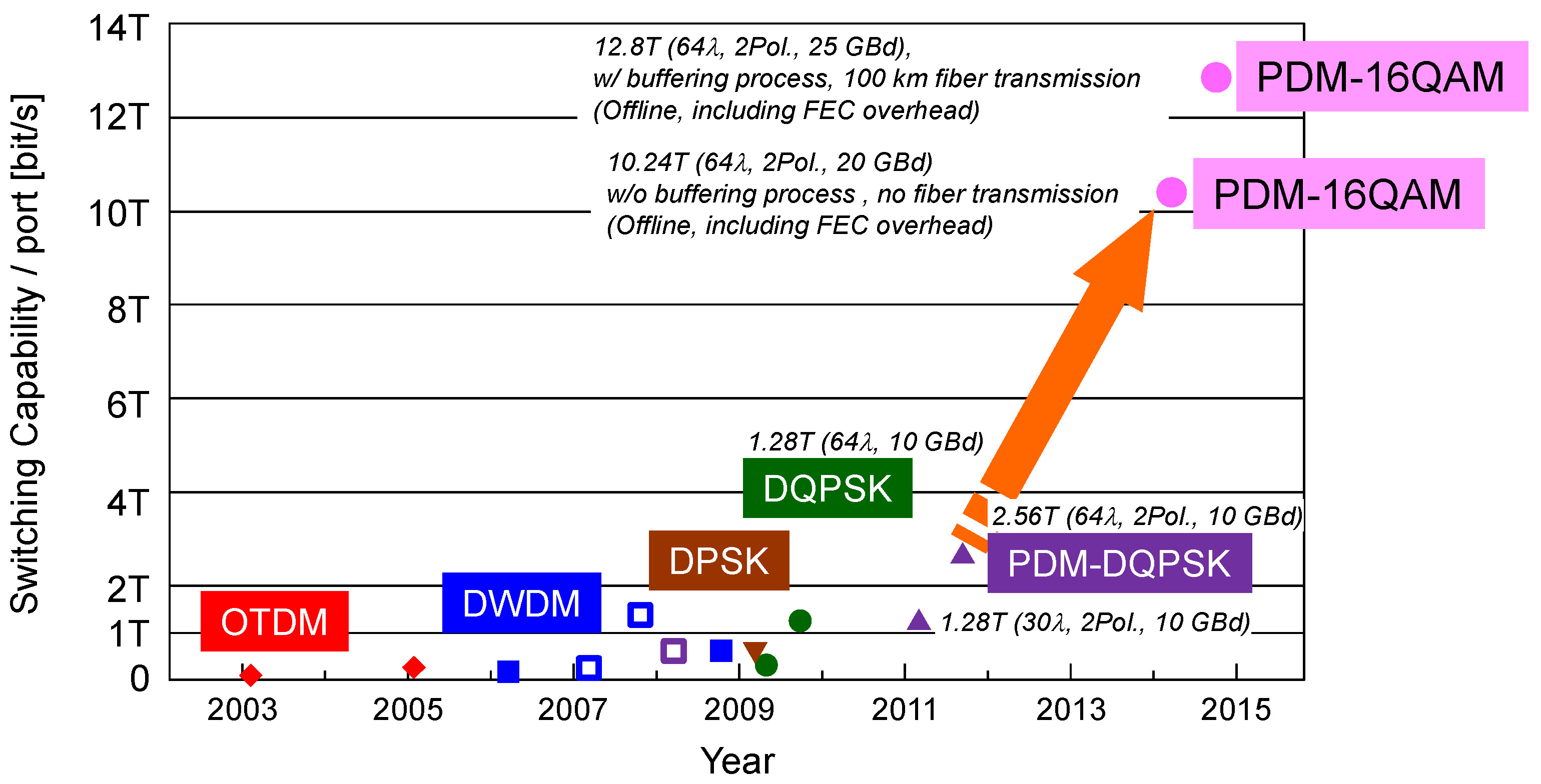
:1. Introduction
2. Coherent Burst-Mode Receivers for PDM-QPSK and PDM-16QAM Modulated Payloads
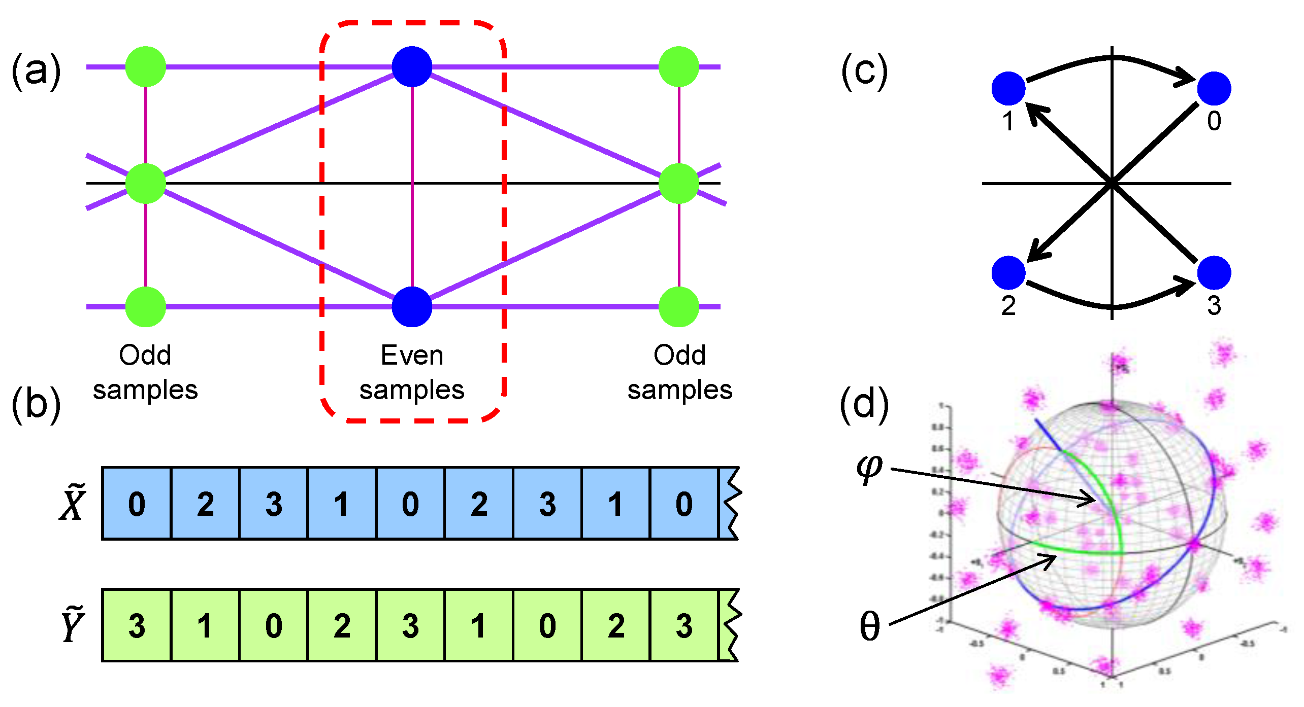
2.1. Coherent Burst-Mode Receiver Based on the Stokes Sphere
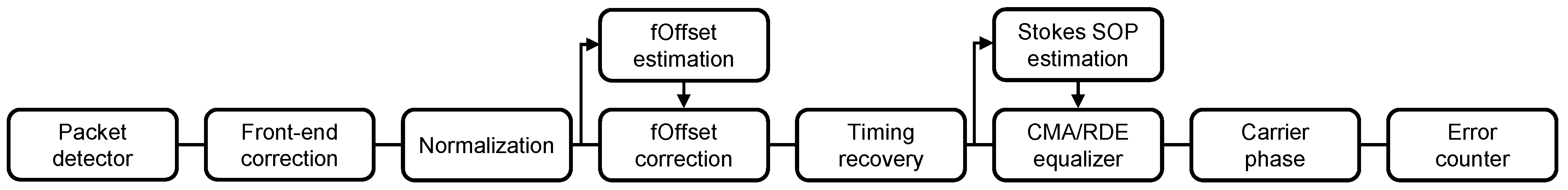
2.2. Digital Coherent Burst-Mode Receiver DSP Stages
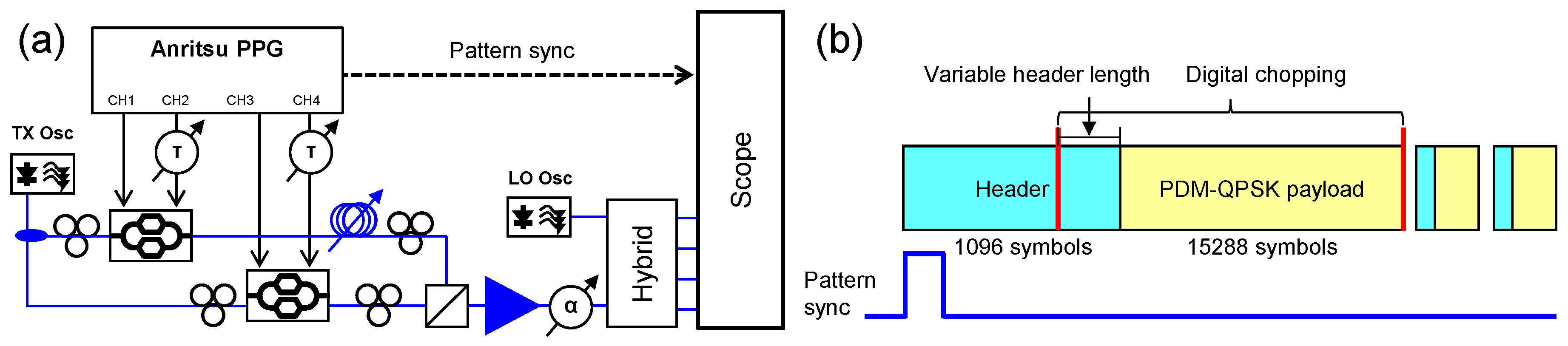
2.3. Digital Coherent Burst-Mode Receiver Experimental Characterization
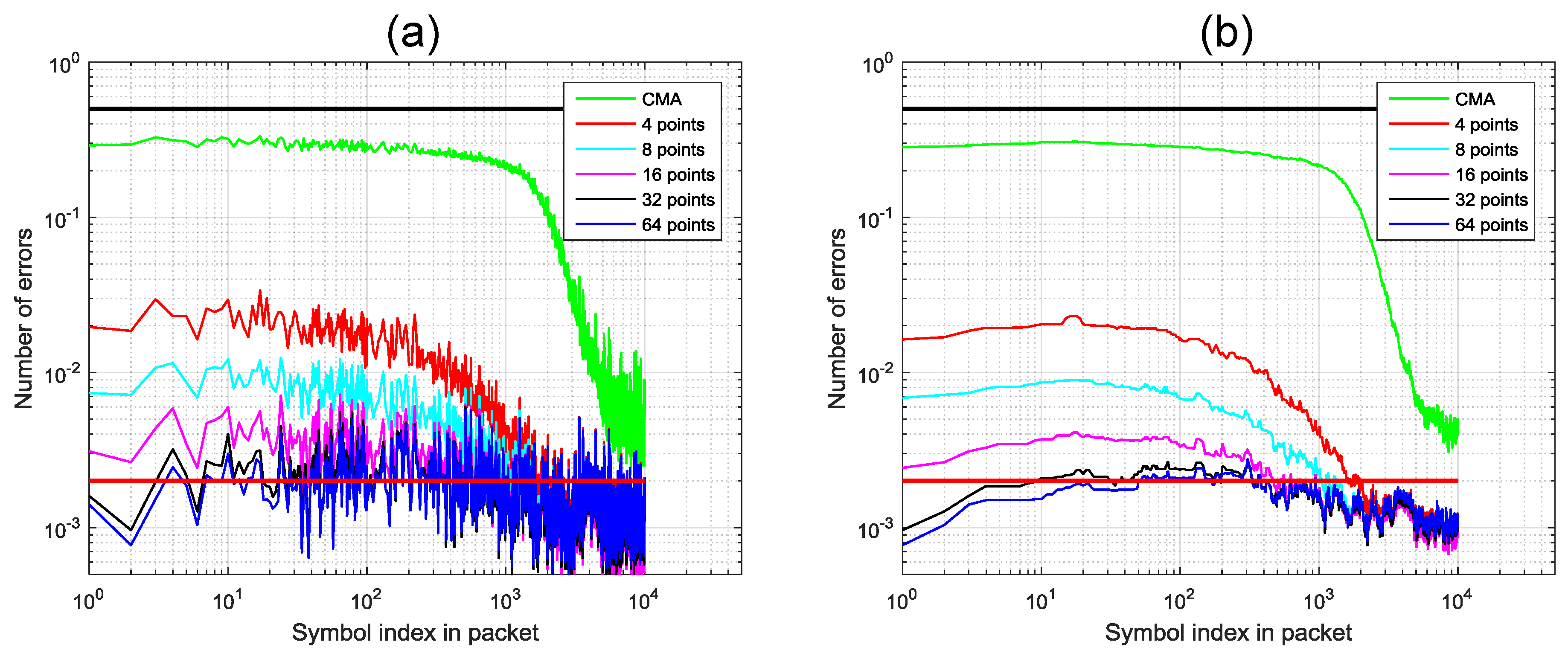
2.4. Methodology and Experimental Results
3. High-Capacity DWDM PDM-16QAM Optical Switch
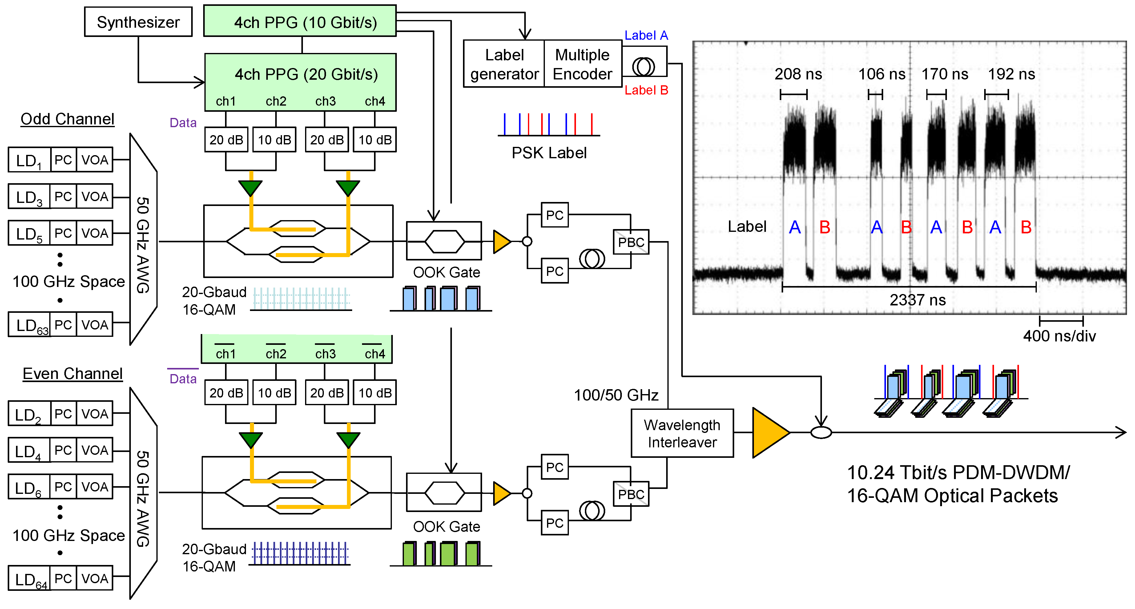
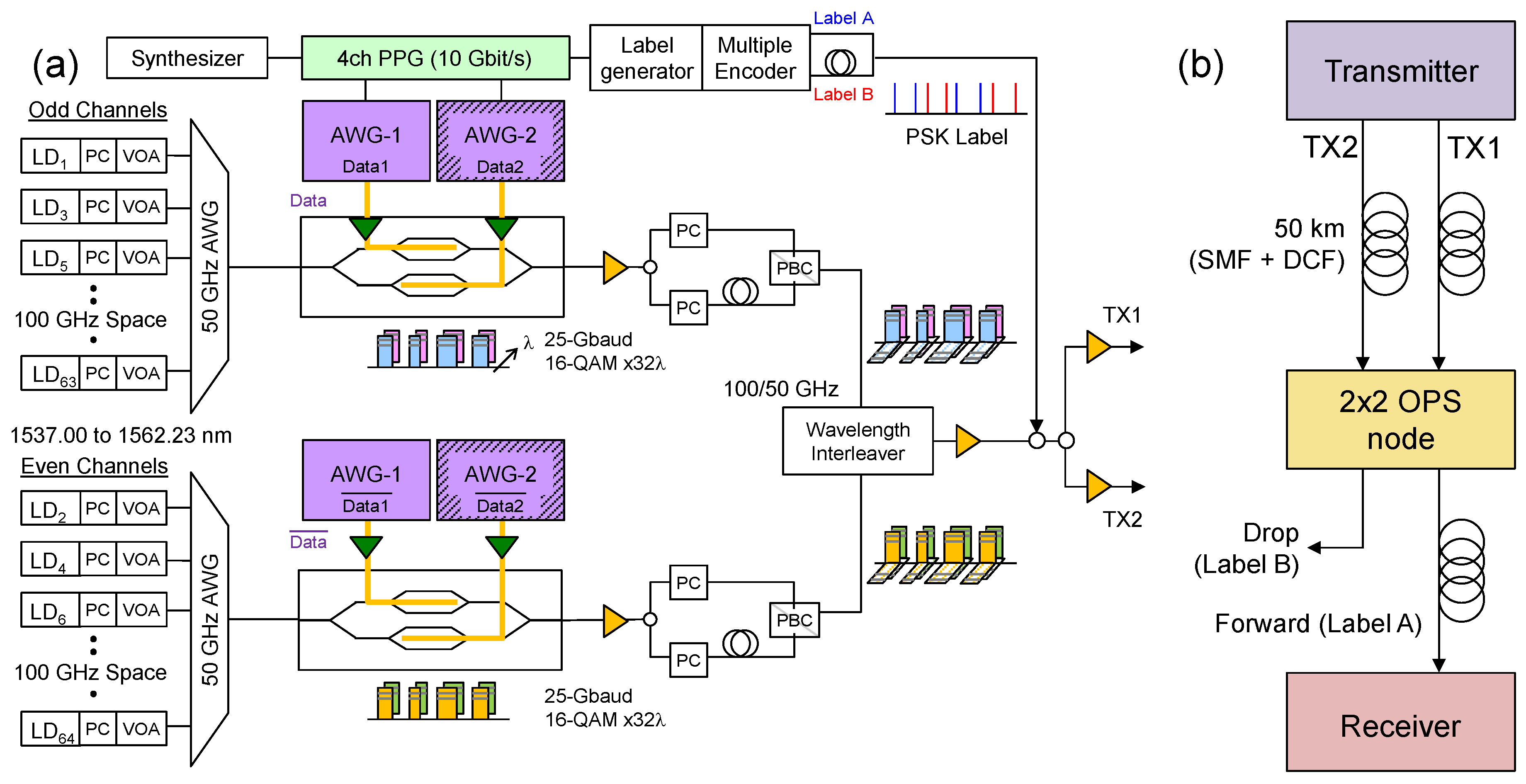
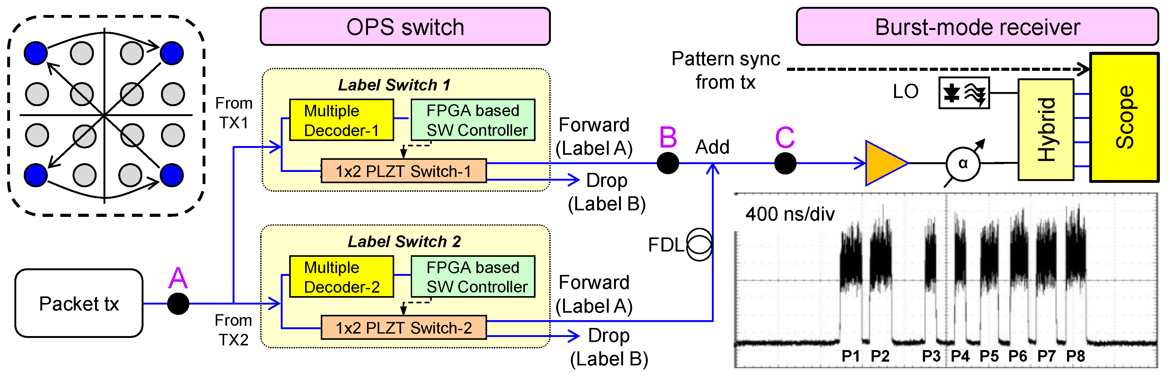
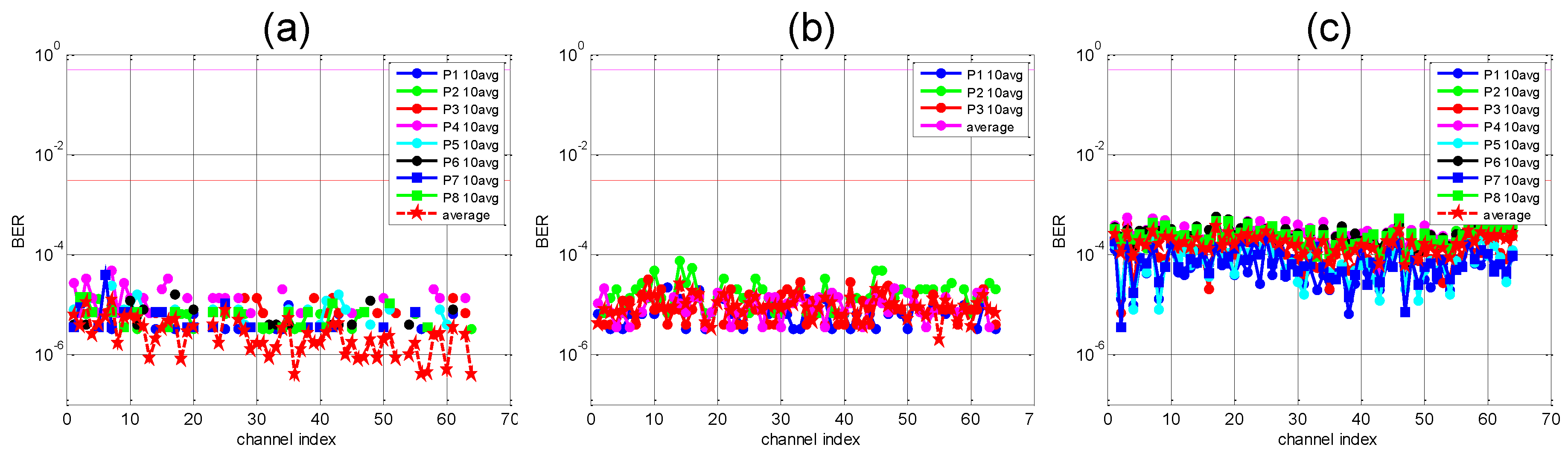
3.1. Experimental Setup
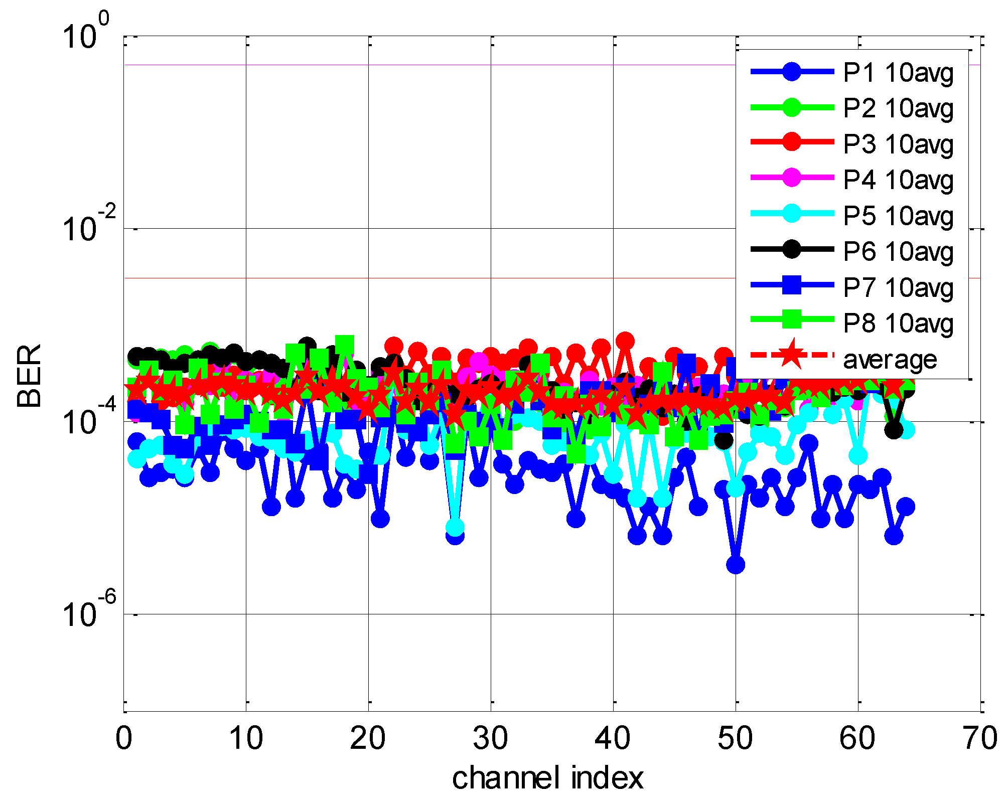
3.2. Experimental Results and Discussion
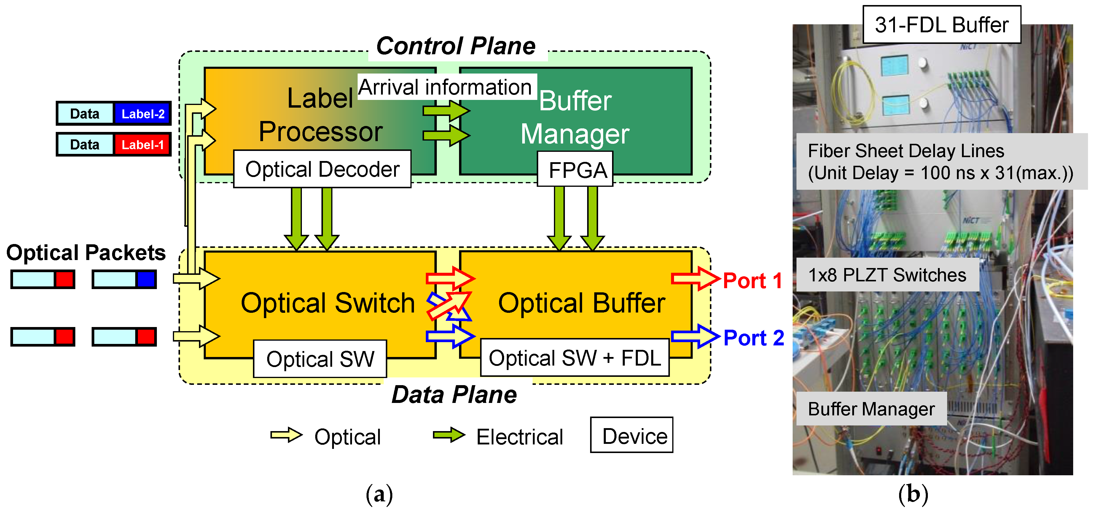
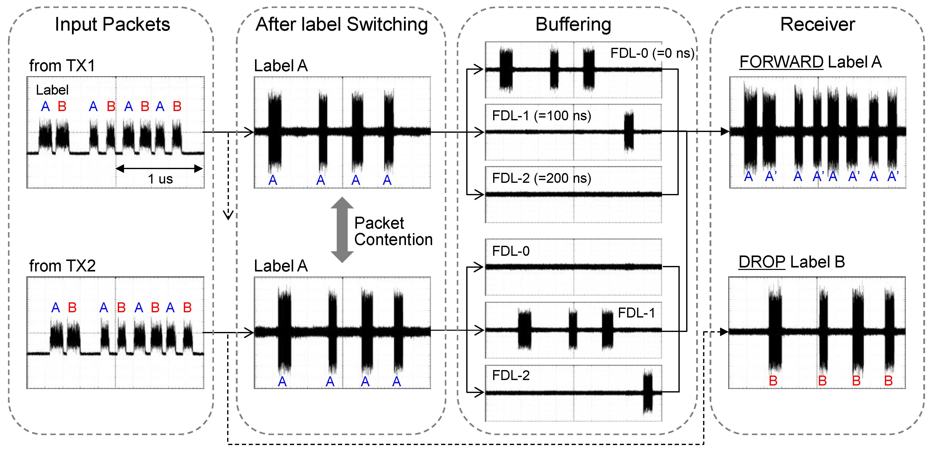
4. High Capacity 2 × 2 OPS Node with Contention Resolution
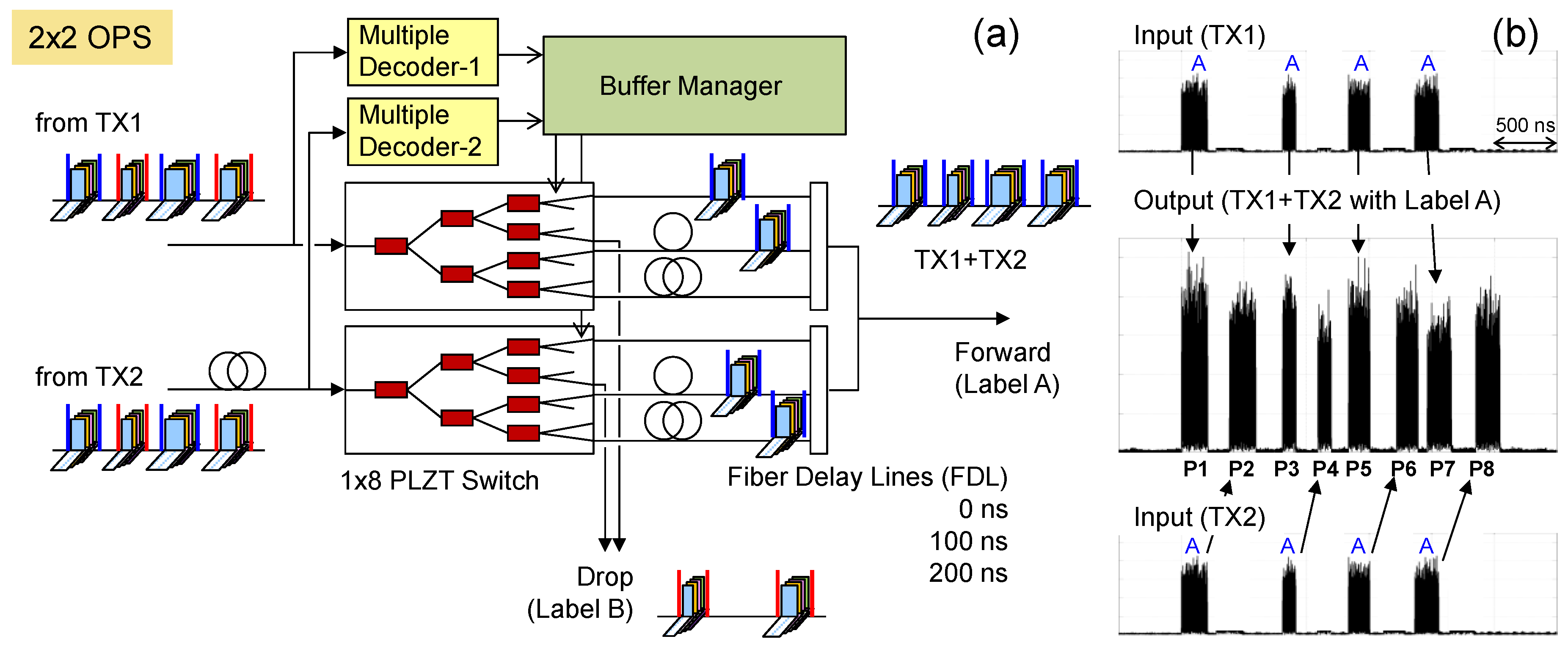
4.1. Switching and Buffering Experimental Setup
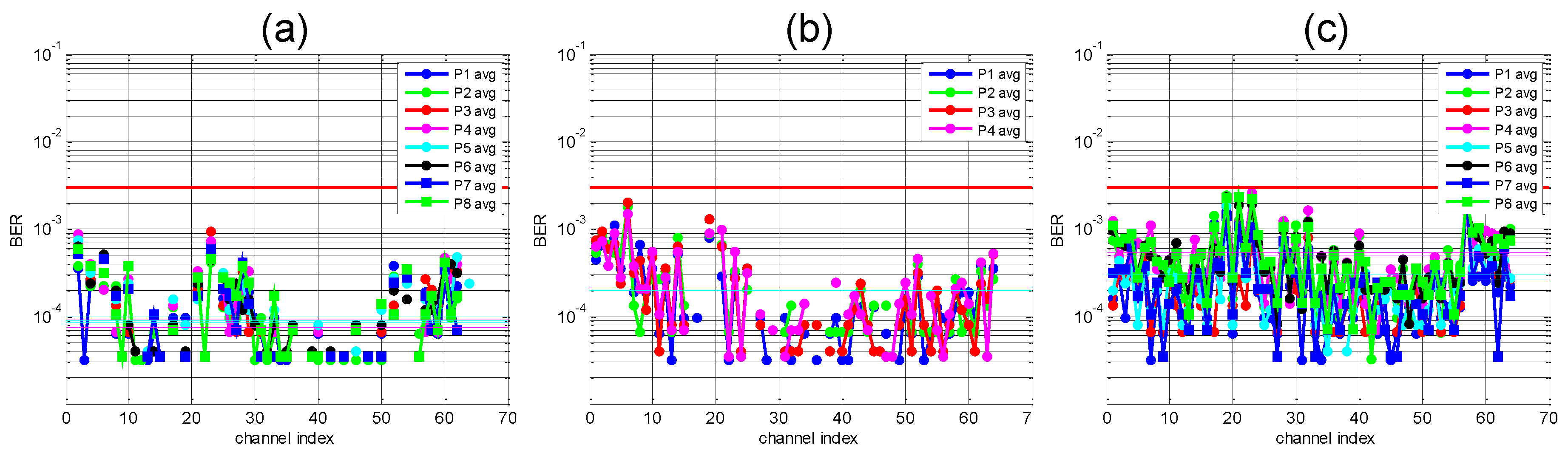
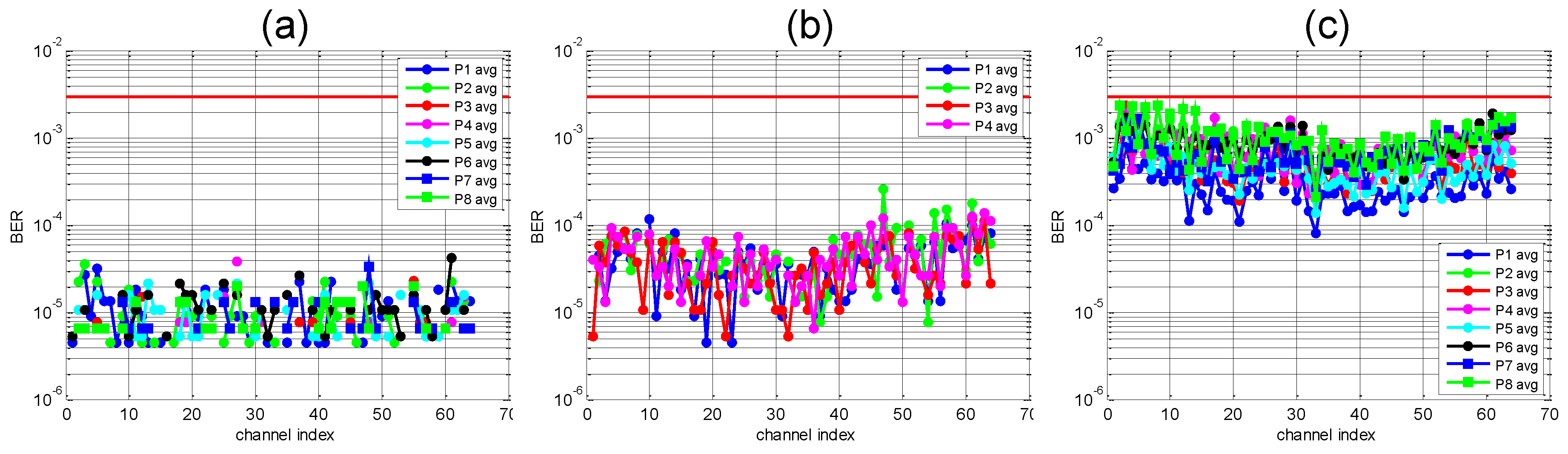
4.2. Experimental Results and Discussion
5. High Capacity 2 × 2 OPS Node with Contention Resolution and Fiber Transmission
5.1. Transmission Experimental Setup
5.2. Packet Switching, Buffering and Transmission Results and Discussion
6. Conclusions
Acknowledgments
Author Contributions
Conflicts of Interest
References
- Ruiz, M.; Lord, A.; Fonseca, D.; Pioro, M.; Wessaly, R.; Fernandez-Palacios, J.P. Planning Fixed to Flexgrid Gradual Migration: Drivers and Open Issues. IEEE Commun. Mag. 2014, 52, 70–76. [Google Scholar] [CrossRef]
- Tomkos, I.; Azodolmolky, S.; Sole-Pareta, J.; Careglio, D.; Palkopoulou, E. A Tutorial on the Flexible Optical Networking Paradigm: State of the Art, Trends, and Research Challenges. Proc. IEEE 2014, 102, 1317–1337. [Google Scholar] [CrossRef]
- Tanenbaum, A.S. Computer Networks, 4rd ed.; Prentice Hall: Upper Saddle River, NJ, USA, 2002. [Google Scholar]
- Furukawa, H.; Miyazawa, T.; Wada, N.; Harai, H. Moving the boundary between wavelength resources in optical packet and circuit integrated ring network. Opt. Express 2014, 22, 47–54. [Google Scholar] [CrossRef] [PubMed]
- Zapata-Beghelli, A.; Bayvel, P. Dynamic versus Static Wavelength-Routed Optical Networks. J. Lightwave Technol. 2008, 26, 3403–3415. [Google Scholar] [CrossRef]
- Cisco Systems, Inc. The Zettabyte Era: Trends and Analysis. In White Paper; Cisco Systems, Inc.: San Jose, CA, USA, 2016. [Google Scholar]
- Jue, J.P.; Yang, W.-H.; Kim, Y.-C.; Zhang, Q. Optical packet and burst switched networks: A review. IET Commun. 2009, 3, 334–352. [Google Scholar] [CrossRef]
- Amaya, N.; Irfan, M.; Zervas, G.; Nejabati, R.; Simeonidou, D.; Sakaguchi, J.; Klaus, W.; Puttnam, B.J.; Miyazawa, T.; Awaji, Y.; et al. Fully-elastic multi-granular network with space/frequency/time switching using multi-core fibres and programmable optical nodes. Opt. Express 2013, 21, 8865–8872. [Google Scholar] [CrossRef] [PubMed]
- Effenberger, F.; El-Bawab, T.S. Passive Optical Networks: Past, present, and future. Opt. Switch. Netw. 2009, 6, 143–150. [Google Scholar] [CrossRef]
- Miao, W.; Yin, X.; Bauwelinck, J.; Dorren, H.; Calabretta, N. Performance Assessment of Optical Packet Switching System with Burst-mode Receivers for Intra-data Center Networks. In Proceedings of the Optical Fiber Communications Conference (OFC), San Francisco, CA, USA, 9–13 March 2014. [Google Scholar]
- Mestre, M.A.; de Valicourt, G.; Jenneve, P.; Mardoyan, H.; Bigo, S.; Pointurier, Y. Optical Slot Switching-Based Datacenters with Elastic Burst-Mode Coherent Transponders. In Proceedings of the European Conference on Optical Communications (ECOC), Cannes, France, 21–25 September 2014. [Google Scholar]
- Nashimoto, K.; Kudzuma, D.; Han, H. Nano-Second Response, Polarization Insensitive and Low-Power Consumption PLZT 4 × 4 Matrix Optical Switch. In Proceedings of the Optical Fiber Communications Conference (OFC), Los Angeles, CA, USA, 6–10 March 2011. [Google Scholar]
- Shinada, S.; Furukawa, H.; Nakamura, M.; Wada, N. Record Switching Throughput of 1.28 Tb/s/port (64-wavelength × 20-Gbit/s) by DWDM/NRZ-DQPSK Optical Packet Switching. In Proceedings of the European Conference on Optical Communications (ECOC), Vienna, Austria, 20–24 September 2009. [Google Scholar]
- Shinada, S.; Furukawa, H.; Wada, N. Over 1-Tbit/s/port Polarization-Multiplexed DWDM/DQPSK Optical Packet Switching and Buffering. In Proceedings of the Optical Fiber Communications Conference (OFC), Los Angeles, CA, USA, 6–10 March 2011. [Google Scholar]
- Shinada, S.; Furukawa, H.; Wada, N. 2.56 Tbit/s/port Dual-Polarization DWDM/NRZ-DQPSK Optical Packet Switching and Buffering. In Proceedings of the European Conference on Optical Communications (ECOC), Geneva, Switzerland, 18–22 September 2011. [Google Scholar]
- Shinada, S.; Furukawa, H.; Wada, N. Huge capacity optical packet switching and buffering. Opt. Express 2011, 26, B406–B414. [Google Scholar] [CrossRef] [PubMed]
- Delgado Mendinueta, J.M.; Puttnam, B.J.; Luis, R.S.; Shinada, S.; Wada, N. Fast Equalizer Kernel Initialization for Coherent PDM-QPSK Burst-Mode Receivers Based on Stokes Estimator. In Proceedings of the OSA Advanced Photonics, Rio Grande, PR, USA, 14–17 July 2013. [Google Scholar]
- Shinada, S.; Delgado Mendinueta, J.M.; Wada, N. Over 10-Tbit/s/port Optical Packet Switching Using Polarization-Multiplexed DWDM/16-QAM Packets. In Proceedings of the Optical Fiber Communications Conference (OFC), San Francisco, CA, USA, 9–13 March 2014. [Google Scholar]
- Xu, J.; Zhang, X.; Mork, J. Investigation of Patterning Effects in Ultrafast SOA-Based Optical Switches. IEEE J. Quantum Electron. 2010, 46, 87–94. [Google Scholar] [CrossRef]
- Kamitani, N.; Yoshida, Y.; Kitayama, K. Experimental study on impact of SOA nonlinear phase noise in 40Gbps coherent 16QAM transmissions. In Proceedings of the European Conference on Optical Communications (ECOC), Amsterdam, The Netherlands, 16–20 September 2012. [Google Scholar]
- Shinada, S.; Delgado Mendinueta, J.M.; Wada, N. Demonstration of a DWDM Polarization-Division Multiplexing 16QAM Optical Packet Switching Node with Packet Buffering. In Proceedings of the Optoelectronics and Communications Conference (OECC), Melbourne, Australia, 6–10 July 2014. [Google Scholar]
- Shinada, S.; Delgado Mendinueta, J.M.; Luis, R.S.; Wada, N. Operation of a 12.8 Tbit/s DWDM Polarization Division Multiplexing 16-QAM Optical Packet Switching Node after 50 km Fiber Transmission. In Proceedings of the European Conference on Optical Communications (ECOC), Cannes, France, 21–25 September 2014. [Google Scholar]
- Ossieur, P.; Ridder, T.D.; Bauwelinck, J.; Mélange, C.; Baekelandt, B.; Qiu, X.-Z.; Vandewege, J.; Talli, G.; Antony, C.; Townsend, P.; et al. A 10 Gb/s Burst-Mode Receiver with Automatic Reset Generation and Burst Detection for Extended Reach PONs. In Proceedings of the Optical Fiber Communications Conference (OFC), San Diego, CA, USA, 22–26 March 2009. [Google Scholar]
- Poehlmann, W.; Schmuck, H.; Bonk, R.; Pfeiffer, T. First 20 Gbit/s Burst-mode OOK Upstream with Direct Modulated Laser over up to 50 km Single Mode Fiber. Proceedings of IEEE Photonics Networks Conference, Waikoloa, HI, USA, 2–6 October 2016. [Google Scholar]
- Savory, S.J. Digital Coherent Optical Receivers: Algorithms and Subsystems. IEEE J. Sel. Top. Quantum Electron. 2016, 16, 1164–1179. [Google Scholar] [CrossRef]
- Vacondio, F.; Simonneau, C.; Voicila, A.; Dutisseuil, E.; Tanguy, J.-M.; Antona, J.-C.; Charlet, G.; Bigo, S. Real time implementation of packet-by-packet polarization demultiplexing in a 28 Gb/s burst mode coherent receiver. In Proceedings of the Optical Fiber Communications Conference (OFC), Los Angeles, CA, USA, 4–8 March 2012. [Google Scholar]
- Kikuchi, K.; Tsukamoto, S. Evaluation of Sensitivity of the Digital Coherent Receiver. J. Lightwave Technol. 2008, 26, 1817–1822. [Google Scholar] [CrossRef]
- Maher, R.; Millar, D.; Savory, S.; Thomsen, B.J. Widely Tunable Burst Mode Digital Coherent Receiver with Fast Reconfiguration Time for 112 Gb/s DP-QPSK WDM Networks. J. Lightwave Technol. 2012, 30, 3924–3930. [Google Scholar] [CrossRef]
- Geyer, J.; Hauske, F.; Fludger, C.; Duthel, T.; Schulien, C.; Kuschnerov, M.; Piyawanno, K.; van den Borne, D.; Schmidt, E.-D.; Spinnler, B.; et al. Channel parameter estimation for polarization diverse coherent receivers. IEEE Photonics Technol. Lett. 2008, 20, 776–778. [Google Scholar] [CrossRef]
- Hauske, F.; Kuschnerov, M.; Spinnler, B.; Lankl, B. Optical performance monitoring in digital coherent receivers. J. Lightwave Technol. 2009, 27, 3623–3631. [Google Scholar] [CrossRef]
- Agrawal, G.P. Lightwave Technology Telecommunication Systems; John Wiley & Sons: Somerset, NJ, USA, 2005. [Google Scholar]
- Szafraniec, B.; Nebendahl, B.; Marshall, T. Polarization demultiplexing in Stokes space. Opt. Express 2010, 18, 17928–17939. [Google Scholar] [CrossRef] [PubMed]
- Szafraniec, B.; Marshall, T.S.; Nebendahl, B. Performance Monitoring and Measurement Techniques for Coherent Optical Systems. J. Lightwave Technol. 2013, 31, 648–663. [Google Scholar] [CrossRef]
- Borkowski, R.; Zibar, D.; Caballero, A.; Arlunno, V.; Tafur Monroy, I. Optical Modulation Format Recognition in Stokes Space for Digital Coherent Receivers. In Proceedings of the Optical Fiber Communications Conference (OFC), Anaheim, CA, USA, 19–21 March 2013. [Google Scholar]
- Roman, S. Advanced Linear Algebra, 3rd ed.; Springer: New York, NY, USA, 2008. [Google Scholar]
- Delgado Mendinueta, J.M.; Furukawa, H.; Shinada, S.; Wada, N. Multi-rate coherent burst-mode PDM-QPSK optical receiver for flexible optical networks. In Proceedings of the Optoelectronics and Communications Conference (OECC), Niigata, Japan, 3–7 July 2016. [Google Scholar]
- Lee, S.J. A new non-data-aided feedforward symbol timing estimator using two samples per symbol. IEEE Commun. Lett. 2002, 6, 205–207. [Google Scholar]
- Oerder, M.; Meyr, H. Digital Filter and Square Timing Recovery. IEEE Trans. Commun. 1998, 36, 605–612. [Google Scholar] [CrossRef]
- Huang, L.; Lau, A.P.T.; Lu, C.; He, S. Performance analysis of blind timing phase estimators for digital coherent receivers. Opt. Express 2014, 22, 6749–6763. [Google Scholar] [CrossRef] [PubMed]
- Viterbi, A.J.; Viterbi, A.M. Nonlinear Estimation of PSK-modulated carrier Phase with Application to Burst Digital Transmission. IEEE Trans. Inf. Theory 1983, 29, 543–551. [Google Scholar] [CrossRef]
- Fatadin, I.; Ives, D.; Savory, S.J. Laser Linewidth Tolerance for 16-QAM Coherent Optical Systems Using QPSK Partitioning. IEEE Photonics Technol. Lett. 2010, 22, 631–633. [Google Scholar] [CrossRef]
- Cincotti, G.; Wada, N.; Kitayama, K. Characterization of a full encoder/decoder in the AWG configuration for code-based photonic routers—Part I: Modeling and Design. J. Lightwave Technol. 2006, 24, 103–112. [Google Scholar] [CrossRef]
- Wada, N.; Cincotti, G.; Yoshima, S.; Kataoka, N.; Kitayama, K. Characterization of a full encoder/decoder in the AWG configuration for code-based photonic routers—Part II: Experiments and applications. J. Lightwave Technol. 2006, 24, 113–121. [Google Scholar] [CrossRef]
- Shinada, S.; Furukawa, H.; Wada, N. Demonstration of Flexible Optical Buffer based on 1 × 32 Optical Switches and Fiber-Sheet Delay Lines. In Proceedings of the Optical Fiber Communications Conference (OFC), Anaheim, CA, USA, 19–21 March 2013. [Google Scholar]
- Shinada, S.; Furukawa, H.; Wada, N. Investigation of Optical Buffer Capacity using Large-scale Fiber Delay Lines for Variable-length Optical Packet Switching. In Proceedings of the European Conference on Optical Communications (ECOC), London, UK, 22–26 September 2013. [Google Scholar]
- Wang, J.; Speidel, J. 16QAM Symbol Timing Recovery in the Upstream Transmission of DOCSIS Standard. IEEE Trans. Broadcast. 2003, 49, 211–216. [Google Scholar] [CrossRef]


© 2017 by the authors. Licensee MDPI, Basel, Switzerland. This article is an open access article distributed under the terms and conditions of the Creative Commons Attribution (CC BY) license (http://creativecommons.org/licenses/by/4.0/).
Share and Cite
Delgado Mendinueta, J.M.; Shinada, S.; Furukawa, H.; Wada, N. Ultra-High-Capacity Optical Packet Switching Networks with Coherent Polarization Division Multiplexing QPSK/16QAM Modulation Formats. Photonics 2017, 4, 27. https://doi.org/10.3390/photonics4020027
Delgado Mendinueta JM, Shinada S, Furukawa H, Wada N. Ultra-High-Capacity Optical Packet Switching Networks with Coherent Polarization Division Multiplexing QPSK/16QAM Modulation Formats. Photonics. 2017; 4(2):27. https://doi.org/10.3390/photonics4020027
Chicago/Turabian StyleDelgado Mendinueta, José Manuel, Satoshi Shinada, Hideaki Furukawa, and Naoya Wada. 2017. "Ultra-High-Capacity Optical Packet Switching Networks with Coherent Polarization Division Multiplexing QPSK/16QAM Modulation Formats" Photonics 4, no. 2: 27. https://doi.org/10.3390/photonics4020027