Design Rules For a Nano-Opto-Mechanical Actuator Based on Suspended Slot Waveguides


Photonics Research Group, Dipartimento di Ingegneria Elettrica e dell’Informazione, Politecnico di Bari, via E. Orabona n. 4, Bari 70125, Italy
*
Author to whom correspondence should be addressed.
Photonics 2017, 4(3), 43; https://doi.org/10.3390/photonics4030043
Submission received: 28 July 2017
/
Revised: 29 August 2017
/
Accepted: 30 August 2017
/
Published: 1 September 2017
Abstract
:In this paper, physical modeling including optical and Casimir forces is adopted in order to analyze a nano-opto-mechanical actuator based on silicon-on-insulator suspended slot waveguides. Numerical simulations based on the finite element method and systematic design rules are presented. Moreover, parametric investigations on slot waveguide sizes and optical properties are presented, and their influence on the actuator’s features are discussed.
1. Introduction
Optical forces can be generally divided into two major categories, i.e., radiation pressure and transverse gradient forces. The former acts along the light propagation direction and can be used for the self-cooling of a micromechanical resonator [1], for measurements of high-power laser emission [2], and for the realization of micro-mechanical oscillators [3] and optical actuators. In 1994, Higurashi et al. [4] experimentally demonstrated the rotative motion of micro-objects driven by radiation pressure, at 22 rpm, with a laser pump of 80 mW.
On the contrary, the gradient optical force acts transversely to the propagation direction of the light and can be used for optical switching [5], nano-opto-mechanical actuators [6], and tunable optical coupling [7]. From simulations on a nano-opto-mechanical actuator in Reference [6], driven by the gradient optical force, a force per unit length of 1.8 pN μm−1 mW−1 was evaluated, which is much higher than the force produced by a typical comb drive actuator. The optically-induced force between coupled high-Q whispering gallery modes of microsphere resonators was theoretically calculated in Reference [8], in which attractive and repulsive forces were found, depending on whether the bi-sphere mode was symmetric or antisymmetric. Moreover, the magnitude of the force was demonstrated to be linearly proportional to the resonator quality factor. The use of microcavity resonances as a general mean of synthesizing optomechanical potentials through the action of optical forces was proposed in Reference [9], showing all-optical functionalities when photonic elements are allowed to freely adapt in response to these optical forces. The result is a new class of self-adaptive photonic devices that facilitate ‘corralling’ and ‘trapping’ of microcavity resonances with light. However, a general analytical formalism capable of handling such complex optical systems is therefore essential in tailoring optical forces at nanoscales. Generally speaking, the knowledge of the full electromagnetic field distribution in such opto-mechanical systems is necessary in order to rigorously evaluate the optical forces by means of the Maxwell stress-tensor (MST). Although the MST method is reliable, it requires large computational efforts, reducing the efficiency in the first stage of the the design for this type of opto-mechanical system. To overcome this bottleneck, several works have been proposed in the literature with the aim of developing a simplified analytical approach [10,11,12]. Despite the different mathematical approach used to evaluate the optical forces, it is typically believed that this gradient force can induce the displacement of integrated nanophotonic structures useful for a number of applications such as nanoactuators, nanotweezers, nanopositioning, and nanosensors as biological, chemical, and physical sensors. In this context, the gradient optical force, through the strong evanescent coupling between two parallel nanophotonic waveguides, was utilized to realize a nano-optical linear actuator [6]. The device performance was theoretically investigated under the condition of optical force uniformly distributed along the waveguide. However, in the nanometer-scale range, the Casimir force is not negligible between uncharged materials, which may cause problems such as stiction [13,14,15], possibly leading to collapse and adhesion between movable parts during the fabrication process. In this sense, the contribution presented by this work is a systematic study to outline the fundamental design rules for a nano-opto-mechanical actuator based on silicon-on-insulator (SOI) suspended slot waveguides, since the work cited in literature [6] only analyzes the actuator performances for a well-defined waveguide cross-section, and neglects the influence of the Casimir force. On the contrary, the goal of this paper is to propose, starting from the device architecture similar to that presented in Reference [6], a number of parametric simulations to determine the design guidelines for a nano-opto-mechanical actuator, in order to predict both the functionality range and the fabrication constrains. The paper is organized as follows. In Section 2, we describe the basic equations to study the mechanical deformation under the influence of both Casimir and optical forces. The proposed equations are numerically solved in order to take into account the load distribution variation along the waveguide length due to its own displacement, representing the main difference from the numerical results proposed in Reference [6], in which only optical force is supposed, acting as a uniform load. In Section 3, a number of numerical results are shown. Moreover, a parametric study to select the fundamental design rules for the opto-mechanical device is carried out. Performances in terms of critical optical power, maximum actuator deflection, and threshold slot gap are evaluated for different SOI suspended slot waveguides. Finally, Section 4 summarizes the conclusions.
2. Design and Theoretical Analysis
In this section, we propose the physical model for the analysis and design of a nano-opto-machanical linear actuator based on SOI technology. The proposed model is based on the Euler-Bernoulli beam equation in which the load is constituted by both optical and Casimir forces. It is worth to noting that, although the device considered in this work is very similar to those proposed in Reference [6], the design rules obtained from our analysis induce specific constraints not evidenced there. The reasons for this difference are essentially related to the previous paper’s assumption that the optical forces act on the waveguide as a uniformly distributed load. Secondly, the analysis proposed in Reference [6] neglects the influence of Casimir forces.
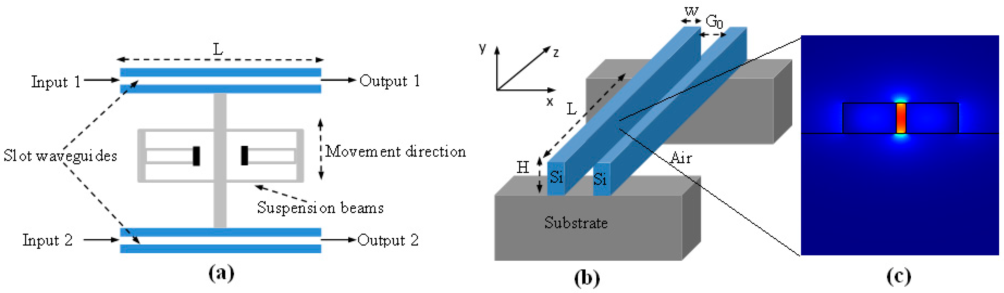
In our analysis, we assume the architecture as sketched in Figure 1a, in which two slot waveguides are suspended in the air for a length of to allow them to bend/deflect as the input optical driving power to the actuator is varied. In Figure 1b, the slot waveguide cross-section is sketched, showing the main geometrical parameters, including the silicon rib width , the slot waveguide height , and the slot width (gap) . Furthermore, in the proposed design procedure, the silicon slot waveguide geometrical dimensions are considered as variable parameters, to be optimized to induce the actuator deflection, according to design rules that will be presented in this work.
In References [8,11], the authors showed that two adjacent waveguides experience forces between them, which are due to the dipole moments induced by the guided light intensity; such forces may be either attractive or repulsive, depending on the phase of the dipoles as induced by the optical properties and the geometrical parameters of the waveguides. Generally speaking, when two optical waveguides are placed close to each other, two kinds of optical eigenmodes can be induced in the overall structure. For lower than a well-determined value (), depending on the refractive index distribution, the two optical waveguides act as a slot structure with the optical mode confined inside the slot region (see Figure 1c). Indeed, as a result of the continuity of the normal component of the electric displacement vector () at the slot interface, a factor proportional to (with being the silicon refractive index) between the values of at both sides of the interface is obtained, inducing an enhancement of the attractive optical force. On the contrary, for , the optical modes are mainly confined in the silicon regions. In this context, the attractive and repulsive optical forces will be generated by the symmetric and anti-symmetric eigenmodes, respectively. Thus, in this sense, a suspended section of a slot waveguide, deprived from the substrate, may induce significant actuator deflection as a result of the strong optical confinement achieved by the high index contrast between Si and air. With reference to Figure 1b, the silicon wires of the slot waveguide are fixed at their ends, forming a movable structure of two parallel double-clamped beams separated by an initial gap of . The deformation distributions , in the direction, along the waveguide direction , can be obtained through the Euler-Bernoulli beam equation for distributed loads:
where is the Young’s Modulus, and is moment of inertia given by .
The terms and represent the optical and the Casimir forces acting in the slot region.
According to References [10,11], the optical force between slot waveguide sides can be calculated directly from its dispersion diagram as:
where is the total power transmitted through the slot waveguide, is the angular frequency of the optical wave, and is the speed of light in vacuum. The term is the effective refractive index of the optical slot mode.
In order to make an estimation, one may express the Casimir force () between two real material plates in terms of the original Casimir force between two perfectly conducting plates separated by a gap distance as [13,14,15]:
where h is the Planck constant, and A is the area of the plates.
It is worth noting that in Equation (1) the load induced by both optical and Casimir forces is distributed non-uniformly. Indeed, starting from an initial static equilibrium, the optical and Casimir forces along the slot waveguide length are constant and assume a value determined by the initial slot width . Under this condition, the slot waveguide deforms according to the boundary conditions for the double-clamped beams: ; , inducing a maximum displacement at the middle of the waveguide. In this context, as the waveguide starts to deform, the forces become non-uniformly distributed, loading the structure with forces that are deformation-dependent by means of the relationship:
Thus, Equations (1)–(4) require a numerical solution based on the finite element method. This aspect represents the main difference from the design rules proposed in Reference [6], in which a uniform optical force is assumed. Under this assumption, the waveguide deformation is given by the theoretical expression:
Equation (5) clearly indicates that the waveguide deformation, at any point, is directly proportional to the optical power, . Thus, no constraint is present on the maximum value that the input optical power can assume. On the contrary, as demonstrated in Reference [15], a critical value for the optical power exists, indicating the limit above which structure collapse occurs.
3. Simulations, Results, and Discussion
The goal of this section is to analyze the features of the waveguide deformation by means of a numerical solution of the equations described in the previous section. By this way, it will be possible to determine the design guidelines for a nano-opto-mechanical actuator based on suspended SOI slot waveguides. In this context, the aim of the optimization procedure is to set the couple ( and the ratio ) for which it is possible to obtain a larger actuator deflection without inducing the collapse of the slot structure. First, the algorithmic procedure for the calculation of optical forces for different slot widths was implemented and investigated in detail using a full-vectorial finite element method (FEM) [16]. With the aim of realizing self-consistent simulations, we implemented an integrated algorithmic procedure based on home-made code and commercial software using a full-vectorial FEM. In particular, for a given value of the ratio , the effective refractive index as a function of the slot width at the operative wavelength was evaluated as a first step, by means of FEM simulations. Thus, the optical and Casimir forces were numerically calculated as a function of the slot width according to Equations (2) and (3), by using the FEM results obtained in the first step. Once the optical and Casimir forces as a function of were evaluated, their dependence from could be found by Equation (4). At this step, Equation (1) was used to calculate the deformation distribution along the slot waveguide length, according to the boundary conditions for the double-clamped beams.
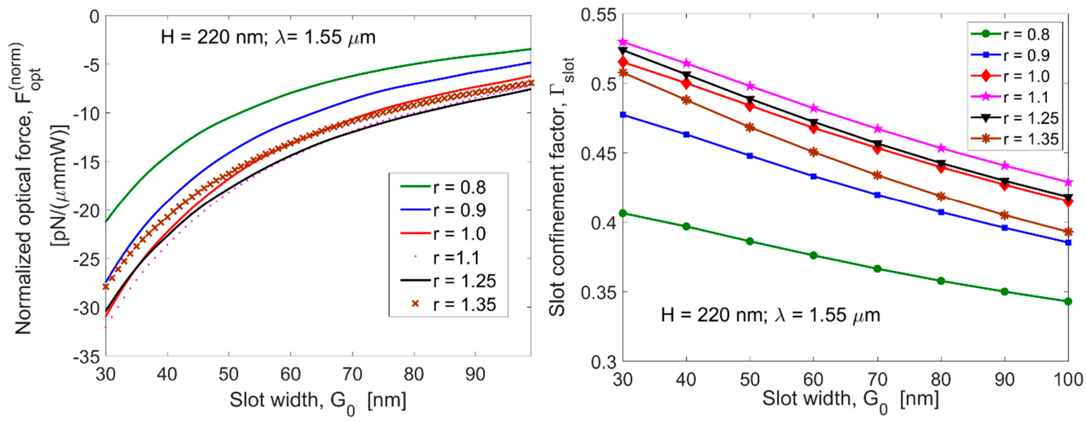
Numerical simulations were performed in order to calculate the E-Field spatial distributions of the quasi-transverse electric (TE) polarized optical mode (see Figure 1c) and the effective refractive index as a function of the slot width and the ratio at the operative wavelength λ = 1.55 μm. According to Equation (2), Figure 2a shows the normalized optical force () as a function of and for different values of , assuming = 220 nm, and = 1.55 µm. For a given value of , the absolute value of the normalized optical force increases by reducing the slot width, as a result of the higher value of the slot confinement factor, (see Figure 2b). Moreover, the plot shows that increases with the ratio up to the value = 1.1. Indeed, for > 1.25, the factor reduces itself, inverting the trend in the optical force.
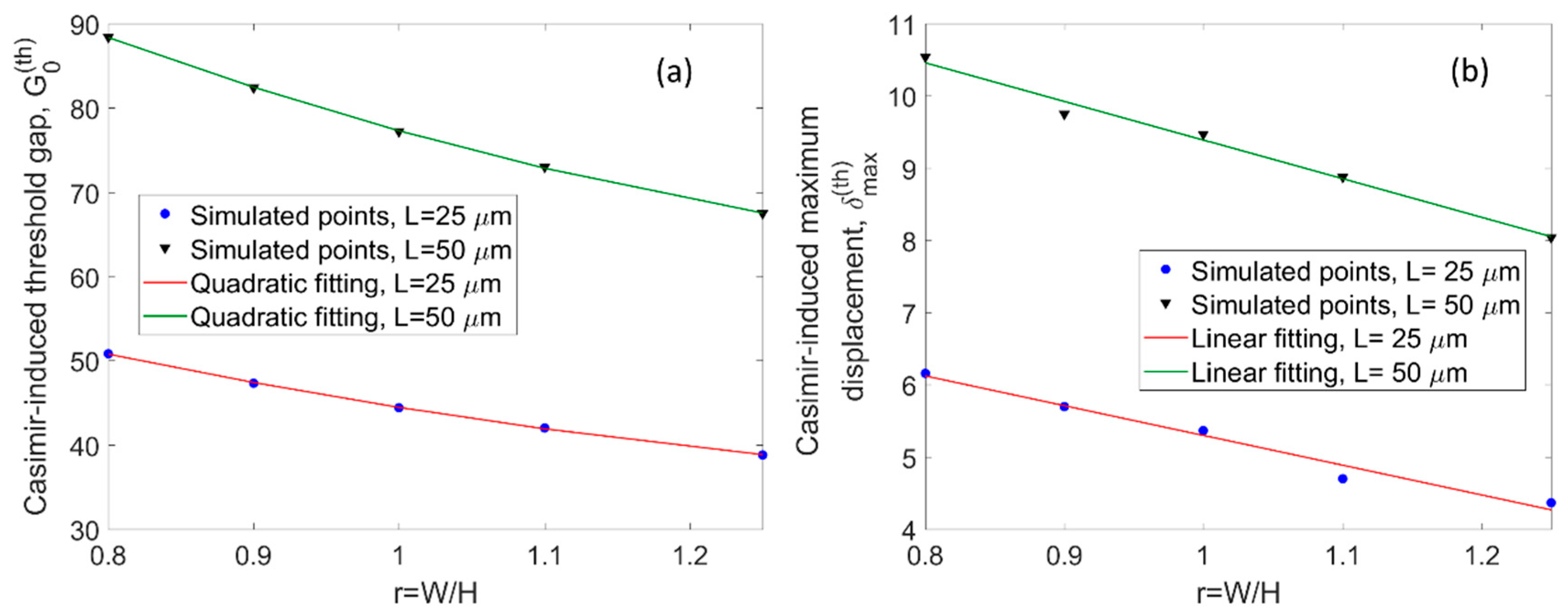
In order to estimate the influence of the Casimir force, we solved Equation (1) with the optical power set at = 0, and considering the non-uniform load as induced by Equation (4). In this context, the numerical solution individuates two different regions separated by a threshold value for the initial slot gap (). Thus for , the structure moves in a stable region. On the contrary, for , the system results unstable, inducing a pre-deformation large enough to cause the structure collapse. In this sense, Figure 3a shows as a function of the ratio , for two different values of the slot waveguide length, . The plot shows that changing the parameter in the range of (0.8–1.25) the gap ranges from 50.8 to 38.8 nm, and from 88.4 to 67.5 nm for length = 25 and µm, respectively. Similarly, in Figure 3b, the maximum displacement relevant to the threshold condition, , is sketched as a function of the ratio , assuming = 25 and µm, respectively.
Since the slot waveguides, as sketched in Figure 1b, can be assimilated to double-clamped beams, the parameter was numerically evaluated to be when . Figure 3b indicates that a not negligible pre-deformation occurs even without optical forces, having in the range from 6.1 to 4.3 nm, and from 10.5 to 8 nm, with changing the parameter in the range of (0.8–1.25), and for = 25 and µm, respectively.
In Figure 3, the markers represent the numerically simulated results, and the solid lines indicate the fitting curves, as obtained by means of the following formulas:
In Table 1, the fitting coefficients of Equation (6) are listed for = 25 and µm, respectively.
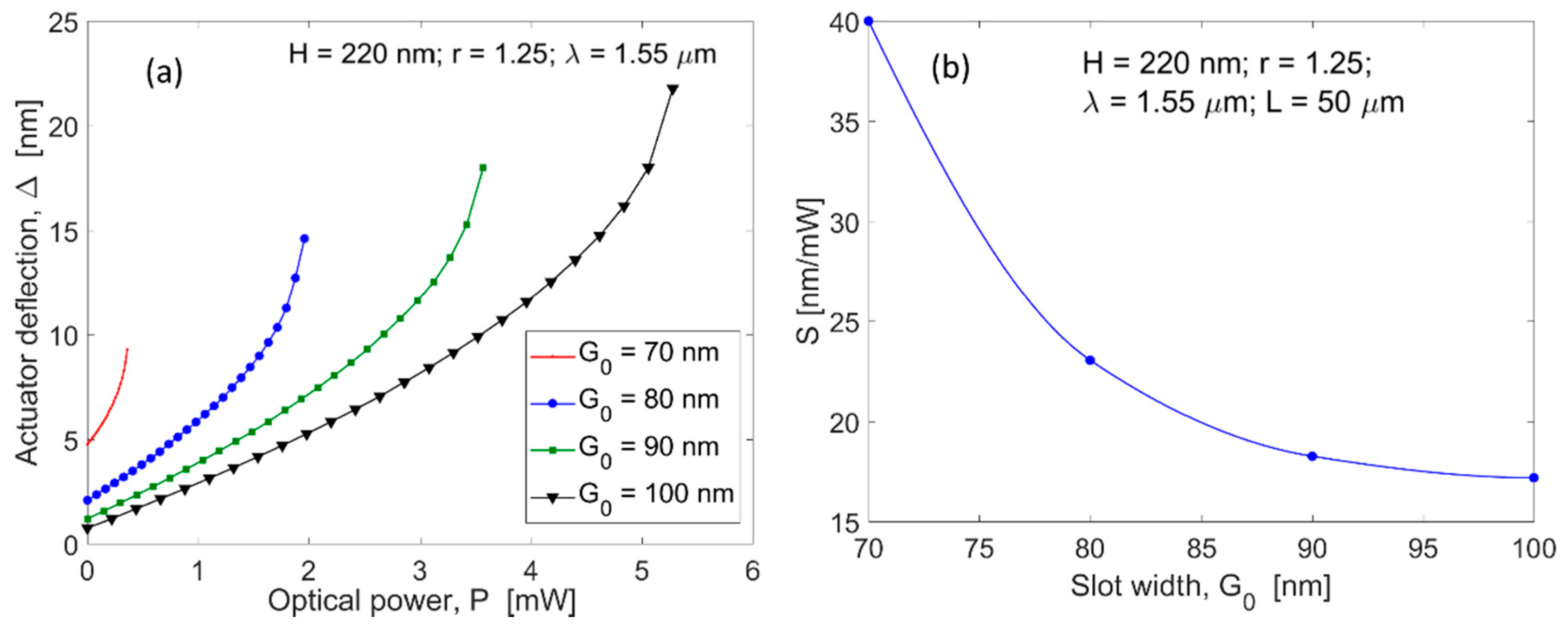
Finally, simulations plotted in Figure 3 with the fitting formulas given by Equation (6) represent a very useful tool to find the design rules for the fabrication of a nano-opto-mechanical actuator. Indeed, this type of analysis allows one to link the definition of the geometry of the suspended slot waveguide directly to the minimum initial slot width () needed to avoid the Casimir-induced structural collapse. At this stage, the actuator deflection, , as induced by the contemporary presence of the Casimir and the optical forces, can be evaluated. Hereafter, the actuator deflection is defined by means of the relationship: . Thus, the interaction between the Casimir and the optical forces with the slot structure is obtained by numerically solving Equations (1)–(4). Moreover, as detailed in Reference [15], increasing the optical power induces the structure to change its equilibrium distribution, according to the increased attractive optical force (see Equation (2)). However, this happens up to a certain maximum value of optical power, named critical power (), where a maximum critical displacement occurs,. Indeed, for , the system becomes unstable, causing the collapse of the suspended slot waveguide sides due to the increasingly stronger attractive optical forces (pull-in effect) [15]. In this context, Figure 4 shows the and as a function of the parameter, assuming = 50 µm, = 100 nm, = 220 nm, and the operative wavelength = 1.55 µm. It is worth noting that the choice of = 100 nm was made due to the need to satisfy the condition for all values of .
The plot evidences that the critical power changes from 1.24 to 5.27 mW, ranging from 0.8 to 1.25. Simultaneously, the displacement ranges from 14.83 to 21.76 nm. Moreover, with the help of Figure 2 and Figure 4, we can conclude that r = 1.25 could represent an efficient choice in order to realize a nano-opto-mechanical actuator based on suspended slot waveguides. In this context, Figure 5a shows the maximum displacement, as a function of the optical power for different values of the initial slot gap , assuming = 50 µm, r = 1.25, = 1.55 µm, and = 220 nm. All curves are plotted up to the relevant critical power value. Thus, only the stable solutions are considered in the plot, indicating that the critical power changes in the range from 0.36 to 5.27 mW, ranging from 70 to 100 nm, and ranging the maximum optical force from 3.6 pN/µm to 81.2 pN/µm. Simultaneously, the actuator deflection ranges from 9.28 to 21.77 nm with a maximum sensitivity changing from 40 to 17.18 nm/mW, as shown in Figure 5b, in which at is plotted as a function of the initial slot gap .
Finally, according to the temperature dependence of the Young’s modulus for silicon given in Reference [17], we estimate that the numerical results presented above suffer from a change of about −1.65%, and 2.3%, ranging the temperature from 25 °C to 150 °C and from −150 °C to 25 °C.
4. Conclusions
The physical model presented in this paper allows the deflection of a nano-opto-mechanical actuator based on SOI technology to be accurately predicted, by taking into account both optical and Casimir forces.
Fitting formulas were derived in order to estimate the minimum slot gap and the related maximum deformation as a function of the ratio between the slot heigth and silicon wire width (H/W), resulting in a very useful tool for the design and fabrication of such opto-mechanical devices, in order to avoid structure collapse. The influence of the suspended slot waveguide sizes and the optical power was rigorously described and evaluated in order to select the stable range for the actuator behavior. Finally, a number of numerical simulations were presented in order to estimate the actuator deflection performance. Although the numerical results based on the non-uniform loads demonstrated the presence of a critical power, above which structure collapse is induced, an actuator deflection of about 21.77 nm at 5.25 mW of optical pump was obtained, indicating the maximum optical force of 81.2 pN/µm.
Author Contributions
F.D.L. applied the opto-mechanical modeling and made the simulations. All the authors wrote the paper and contributed to its discussion and critical reading.
Conflicts of Interest
The authors declare no conflict of interest.
References
- Kippenberg, T.J.; Vahala, K.J. Cavity optomechanics: Back-action at the mesoscale. Science 2008, 321, 1172–1176. [Google Scholar] [CrossRef] [PubMed]
- Williams, P.A.; Hadler, J.A.; Lee, R.; Maring, F.C.; Lehman, J.H. Use of radiation pressure for measurement of high-power laser emission. Opt. Lett. 2013, 38, 4248–4251. [Google Scholar] [CrossRef] [PubMed]
- Rokhsari, H.; Kippenberg, T.J.; Carmon, T.; Vahala, K.J. Radiation-pressure-driven micro-mechanical oscillator. Opt. Express 2005, 13, 5293–5301. [Google Scholar] [CrossRef] [PubMed]
- Higurashi, E.; Ukita, H.; Tanaka, H.; Ohguchi, O. Optically induced rotation of anisotropic micro-objects fabricated by surface micromachining. Appl. Phys. Lett. 1994, 64, 2209. [Google Scholar] [CrossRef]
- Cai, H.; Tao, J.; Ding, L.; Song, J.; Yu, M.; Lo, G.; Kwong, D. Experimental Demonstration of Optical Switch Using Gradient Optical Force. In Proceedings of the OFC/NFOEC, Los Angeles, CA, USA, 4–8 March 2012. [Google Scholar]
- Cai, H.; Xu, K.J.; Tsai, J.M.; Lo, G.Q.; Kwong, D.L.; Liu, A.Q. Nano-Opto-Mechanical Linear Actuator Utilizing Gradient Optical Force. In Proceedings of the 2011 16th International Solid-State Sensors, Actuators and Microsystems Conference, Beijing, China, 5–9 June 2011. [Google Scholar]
- Fong, K.Y.; Pernice, W.H.P.; Li, M.; Tang, H.X. Tunable optical coupler controlled by optical gradient forces. Opt. Express 2011, 19, 15098–15108. [Google Scholar] [CrossRef] [PubMed]
- Povinelli, M.L.; Johnson, S.G.; Lončar, M.; Ibanescu, M.; Smythe, E.J.; Capasso, F.; Joannopoulos, J.D. High-Q enhancement of attractive and repulsive optical forces between coupled whispering gallery-mode resonators. Opt. Express 2005, 13, 8286–8295. [Google Scholar] [CrossRef] [PubMed]
- Rakich, P.T.; Popovic, M.A.; Soljacic, M.; Ippen, E.P. Trapping, corralling and spectral bonding of optical resonances through optically induced potentials. Nat. Photonics 2007, 1, 658–665. [Google Scholar] [CrossRef]
- Ma, J.; Povinelli, M.L. Applications of optomechanical effects for on-chip manipulation of light signals. Solid State Mater. Sci. 2012, 16, 82–90. [Google Scholar] [CrossRef]
- Povinelli, M.L.; Lončar, M.; Ibanescu, M.; Smythe, E.J.; Johnson, S.G.; Capasso, F.; Joannopoulos, J.D. Evanescent-wave bonding between optical waveguides. Opt. Lett. 2005, 30, 3042–3044. [Google Scholar] [CrossRef] [PubMed]
- Rakich, P.T.; Popovic, M.A.; Wang, Z. General Treatment of Optical Forces and Potentials in Mechanically Variable Photonic Systems. Opt. Express 2009, 17, 18116–18135. [Google Scholar] [CrossRef] [PubMed]
- Rodriguez, A.W.; Hui, P.C.; Woolf, D.N.; Johnson, S.G.; Loncar, M.; Capasso, F. Classical and fluctuation-induced electromagnetic interactions in micronscale systems: Designer bonding, antibonding, and Casimir forces. Ann. Phys. 2015, 527, 45–80. [Google Scholar] [CrossRef]
- Dalvit, D.; Milonni, P.; Roberts, D.; Rosa, F.D. Casimir Physics; Springer: Berlin, Germany, 2011; pp. 39–50. [Google Scholar]
- Rodrigues, J.R.; Rosa, F.S.S.; Almeida, V.R. Casimir and Optical Forces Acting on a Silicon NOEMS Device Based on Slot-Waveguide Structure. IEEE Photonics Technol. Lett. 2016, 28, 589–592. [Google Scholar] [CrossRef]
- Comsol Multiphysics, ver. 3.2. Single License; COMSOL Inc.: Stockholm, Sweden, 2005.
- Cho, C.H. Characterization of Young’s modulus of silicon versus temperature using a “beam deflection” method with a four-point bending fixture. Curr. Appl. Phys. 2009, 9, 538–545. [Google Scholar] [CrossRef]
Figure 1.
(a) Schematic architecture of the nano-opto-mechanical actuator; (b) Suspended Si slot waveguide; (c) Slot quasi-transverse electric (TE) mode inducing optical force.
Figure 1.
(a) Schematic architecture of the nano-opto-mechanical actuator; (b) Suspended Si slot waveguide; (c) Slot quasi-transverse electric (TE) mode inducing optical force.

Figure 2.
(a) Slot mode-induced optical force as a function of the slot width, for different values of the parameter; (b) Slot confinement factor as a function of the slot width, for different values of the parameter.
Figure 2.
(a) Slot mode-induced optical force as a function of the slot width, for different values of the parameter; (b) Slot confinement factor as a function of the slot width, for different values of the parameter.

Figure 3.
(a) Casimir-induced threshold gap () as a function of the parameter; (b) Casimir-induced maximum displacement under threshold condition () as a function of the parameter.
Figure 3.
(a) Casimir-induced threshold gap () as a function of the parameter; (b) Casimir-induced maximum displacement under threshold condition () as a function of the parameter.

Figure 4.
Critical power () and maximum critical displacement () as a function of the parameter, assuming = 50 µm, = 100 nm, and = 1.55 µm.
Figure 4.
Critical power () and maximum critical displacement () as a function of the parameter, assuming = 50 µm, = 100 nm, and = 1.55 µm.
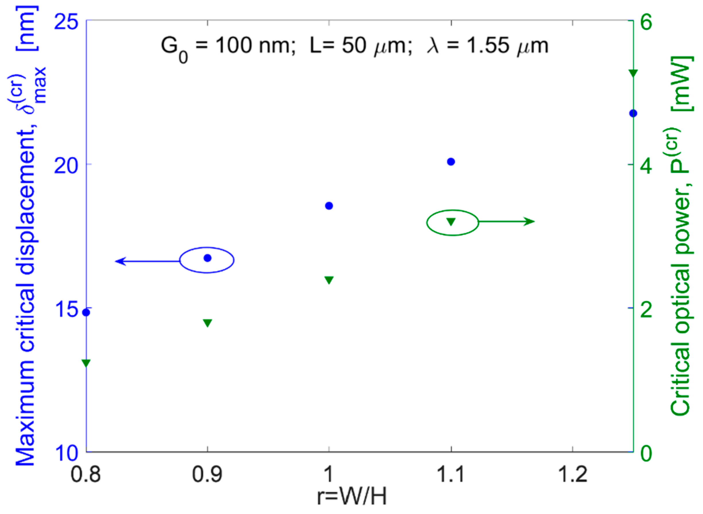
Figure 5.
(a) Actuator deflection as a function of optical power for different values of the initial slot gap; (b) Actuator sensitivity as a function of the initial slot gap.
Figure 5.
(a) Actuator deflection as a function of optical power for different values of the initial slot gap; (b) Actuator sensitivity as a function of the initial slot gap.

Table 1.
Fitting parameters for and .
| (µm) | (nm) | (nm) | (nm) | (nm) | (nm) |
|---|---|---|---|---|---|
| 25 | 20.3546 | −68.1950 | 92.2766 | −4.1165 | 9.4128 |
| 50 | 36.2325 | −120.5132 | 161.5735 | −5.3430 | 14.7322 |
© 2017 by the authors. Licensee MDPI, Basel, Switzerland. This article is an open access article distributed under the terms and conditions of the Creative Commons Attribution (CC BY) license (http://creativecommons.org/licenses/by/4.0/).
Share and Cite
MDPI and ACS Style
De Leonardis, F.; De Carlo, M.; Passaro, V.M.N. Design Rules For a Nano-Opto-Mechanical Actuator Based on Suspended Slot Waveguides. Photonics 2017, 4, 43. https://doi.org/10.3390/photonics4030043
AMA Style
De Leonardis F, De Carlo M, Passaro VMN. Design Rules For a Nano-Opto-Mechanical Actuator Based on Suspended Slot Waveguides. Photonics. 2017; 4(3):43. https://doi.org/10.3390/photonics4030043
Chicago/Turabian StyleDe Leonardis, Francesco, Martino De Carlo, and Vittorio M. N. Passaro. 2017. "Design Rules For a Nano-Opto-Mechanical Actuator Based on Suspended Slot Waveguides" Photonics 4, no. 3: 43. https://doi.org/10.3390/photonics4030043
Note that from the first issue of 2016, this journal uses article numbers instead of page numbers. See further details here.