Aligned Carbon Nanotube Arrays Bonded to Solid Graphite Substrates: Thermal Analysis for Future Device Cooling Applications

1
Air Force Research Laboratory (AFRL), Wright Patterson Air Force Base (AFB), OH 45433, USA
2
Mechanical & Materials Engineering, Wright State University, Dayton, OH 45335, USA
*
Author to whom correspondence should be addressed.
C 2018, 4(2), 28; https://doi.org/10.3390/c4020028
Submission received: 14 February 2018
/
Revised: 3 April 2018
/
Accepted: 10 April 2018
/
Published: 7 May 2018
(This article belongs to the Special Issue Carbon Hybrid Materials)
Abstract
:Carbon nanotubes (CNTs) are known for high thermal conductivity and have potential use as nano-radiators or heat exchangers. This paper focuses on the thermal performance of carpet-like arrays of vertically aligned CNTs on solid graphite substrates with the idea of investigating their behavior as a function of carpet dimensions and predicting their performance as thermal interface material (TIM) for electronic device cooling. Vertically aligned CNTs were grown on highly oriented pyrolytic graphite (HOPG) substrate, which creates a robust and durable all-carbon hierarchical structure. The multi-layer thermal analysis approach using Netzsch laser flash analysis system was used to evaluate their performance as a function of carpet height, from which their thermal properties can be determined. It was seen that the thermal resistance of the CNT array varies linearly with CNT carpet height, providing a unique way of decoupling the properties of the CNT carpet from its interface. This data was used to estimate the thermal conductivity of individual multi-walled nanotube strands in this carpet, which was about 35 W/m-K. The influence of CNT carpet parameters (aerial density, diameter, and length) on thermal resistance of the CNT carpet and its potential advantages and limitations as an integrated TIM are discussed.
1. Introduction
One of the driving forces behind nanotechnology research is its potential to miniaturize electronic devices. As these devices shrink in size and enable more components to be packed into smaller spaces, efficient dissipation of waste heat generated through smaller volumes becomes more challenging to accomplish. Excess heat, if not rapidly dissipated away from the nanoscale electronic components, can lead to signal instabilities and/or premature device degradation. One common issue is failure at the device/substrate interfaces due to thermal expansion mismatch between different interface material compositions. Therefore, optimizing thermal transport through the interface is necessary to ensure stable performance. This calls for new strategies of integrating emerging materials and/or material combinations for future thermal management devices.
Commercially available thermal interface materials (TIM) products, such as solder and thermal grease, have known thermal resistance (R) values of 0.07 × 10⁻⁴ and 0.14 × 10⁻⁴ m2K/W, respectively [1]. However, these materials have limited use in many future aerospace applications due to their high densities, tendency to harden and crack after prolonged usage, and/or environmental degradation [2,3]. Therefore, it is becoming very important to investigate lightweight and robust architectures for TIM that can support the emerging power electronic devices for aerospace use.
Graphene and carbon nanotubes (CNTs) are potential candidates for future microelectronic devices because of their excellent thermal and mechanical properties [4,5,6]. In addition, these carbon materials are tailorable and can be fabricated into highly flexible films that support mechanical compliance in certain electronic packaging materials [7,8]. Carbon materials have lower coefficients of thermal expansion (CTE) values, 1.1 × 10⁻⁶ m/m-K, compared to other commonly used materials for electronics packaging: copper has a CTE value of ~16.6 × 10⁻⁶ m/m-K. It is known that devices or material at the interface layer with CTE mismatch can induce unfavorable condition such as thermomechanical stresses, interface deboning, and microcracking [9]. To avoid such issues, devices should have high thermal conductivity and similar CTEs between all elements composed within the electronic device [10,11,12]. Due to their lower CTE values, carbon materials may address failures due to CTE mismatch while adding mechanical strength and flexibility to the components. In addition, these kinds of components can withstand prolonged thermal cycling and are less prone to failure due to interfacial delamination. Furthermore, carbon materials are chemically inert, which allows these components to operate in more extreme conditions, such as corrosive environments.
Thermal analysis involving carbon materials are very interesting and have many potential advantages. Due to these potential advantages, a variety of carbon containing materials and composite structures has been investigated for thermal applications. Earlier papers have reported thermal analysis of graphene [6,13,14], graphite flakes [10], carbon fillers [15,16], and loose CNTs [15]. However, it must be noted that these types of carbon structures often require additional processing steps such as attachment, assembly, compression bonding, dispersion in a polymer matrix and machining [10]. Moreover, compact solids are prone to CTE mismatch and interfacial mechanics issues. To minimize processing steps, unfavorable defects, and property mismatch concerns, non-compact and compressible three-dimensional structures made of aligned CNT arrays are of particular interest, and the focus of this study. While thermal properties of CNT have been investigated in the past [7,8,9,10,11,12,13,14,15,16,17,18,19,20], the reported data on thermal conductivity can vary over a wide range depending on the test samples and testing conditions. For example, using a dynamic modeling technique, the thermal conductivity (κ) value of a single walled CNT (SWNT) was reported to be 6600 W/m-K [17]. Others have reported κ values with results ranging from 8 to 10,000 W/m-K [18,19,20,21,22,23,24] for SWNTs, and 0.145 to 3000 W/m-K for multi-walled CNTs (MWNTs) [18,22,25,26,27,28,29,30,31]. The wide range of values is a result of differences in the morphology, defects, and testing conditions.
From an electronic packaging standpoint, a detailed understanding of the thermal transport properties of fully assembled CNT carpet on a high-conductivity substrate is more applicable than theoretical properties of individual nanotubes, or clusters of randomly orientated CNTs. Thermal conductivity values of free standing CNTs arrays have been reported to be 1.9 W/m-K for SWNT arrays [18], and 3 to 15 W/m-K for MWNT arrays [28]. These may be a good starting points in terms of the intrinsic thermal behavior, but in a real device, CNT arrays will need to be attached to a substrate. Therefore, a thermal analysis of samples comprised of CNTs arrays attached to their growth substrate is more realistic but also more challenging.
Most studies reporting CNT arrays on substrates have been grown on electronic grade silicon substrates, and reported thermal conductivity (κ) value ranging from 8.3 to 15 W/m-K [27,32]. Others have reported values of 27 W/m-K with the addition of a metallized bonding layer on the CNT array [30]. More recently, studies have reported success with growing CNT arrays on graphite substrates [2,33,34,35]. It has also been suggested that three-dimensional structures consisting of CNTs joined perpendicular to graphite may be suitable as a high-performance TIM [2]. In the latter study, CNT arrays of a fixed length (25 mm) were grown on thin graphite foil, and laser flash analysis (LFA) was used to measure the thermal resistance of the structure. While these studies clearly indicate promise of using these solids as TIM material, there is no scope for separating out the contribution of interfacial thermal resistance from that of the CNT. Properties of the individual CNT must be assumed to estimate the interface, and vice versa. This is a serious limitation because, as mentioned earlier, there is a wide range of reported thermal conductivity values for MWNT spanning over three orders of magnitude (0.145 to 3000 W/m-K). Therefore, any errors on estimating that value can create a very large error in estimates of interfacial property.
The objective of this investigation is to perform thermal measurements on a series of precisely controlled CNT arrays having different carpet heights grown on the same substrate material using a standard set of growth conditions. The advantage of this approach is that the properties of the interface and that CNT carpets can be decoupled to get a better understanding of thermal transport phenomena in these complex geometries. Laser Flash Analysis (LFA) was used to measure the thermal transport properties of such CNT carpet samples in the transverse (through thickness) direction, parallel to CNT arrays. A one-dimensional thermal resistance model was incorporated to investigate the influence of CNT array variables (diameter, array height, and density) on the thermal transport properties of an all carbon system for electronics packaging applications.
2. Experimental
The Substrate used in this study are highly oriented pyrolytic graphite (HOPG) coated with a thin buffer layer of silica film. The HOPG samples were purchased from SPI, Inc. (West Chester, PA, USA), with reported thermal conductivity measurements of 1800 ± 200 W/m-K along the basal plane and 8 ± 2 W/m-K perpendicular to the base plane.
2.1. CNT Growth
Floating catalyst chemical vapor deposition (FCCVD) was used to grow CNT array films on (1 × 1 × 0.1 cm3) HOPG. The details of this growth technique and of its consistent quality has been shown to provide many functional advantages and reported in earlier publications [22,23,24]. The growth parameters were previously established [35]. For this study, the FCCVD growth time was varied to achieve different heights of CNT arrays. The HOPG substrates were first coated with a thin film of SiO2 (<200 nm) as a buffer layer. The SiO2 oxide buffer layer was deposited using microwave plasma CVD, where the silica source was hexamethyldisiloxane, and the procedure was established earlier [36]. The resulting samples were analyzed by scanning electron microscopy (SEM), transmission electron microscopy (TEM), and laser flash analysis (LFA).
2.2. Microscopy
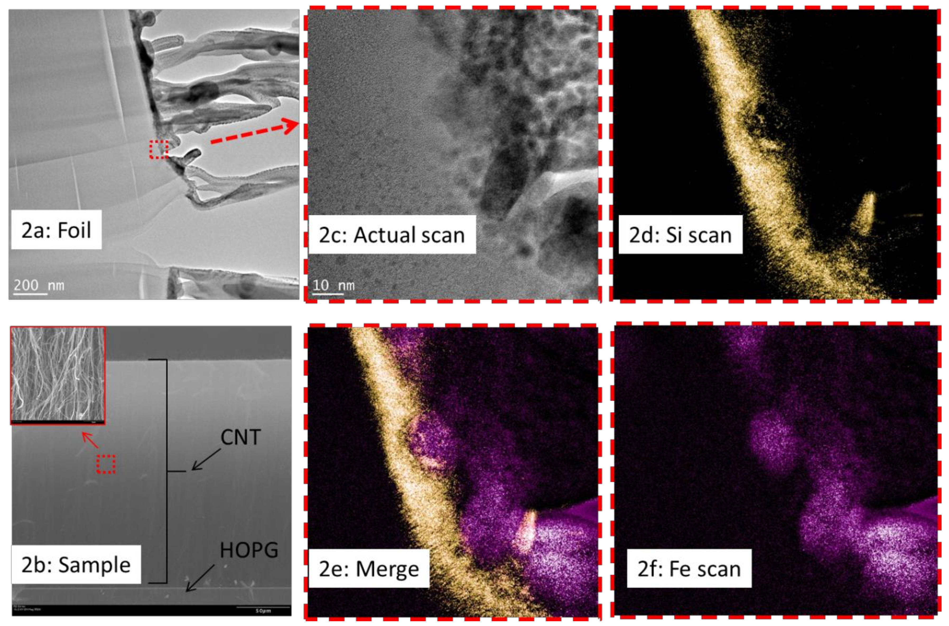
SEM and TEM analysis was performed to characterize the CNTs in relation to morphology, packing density, and interface composition. The TEM foils were prepared using focused ion beam (FIB) extraction and thinning techniques. To make TEM foils, FIB process was used. This technique requires pre-coating the area of interest with sputtered platinum, thereby filling the voids between CNTs and coating the CNT during the process. Once the coating is in place, an ion beam was used to etch away excess material, allowing the area of interest to be lifted for TEM and electron energy loss spectroscopy analyses. The resulting foil was extremely delicate and easily damaged by the high intensity TEM beam. Hence, the images of regions of interest had to be quickly taken after all the focusing adjustments were made on an adjacent area of the specimen. Electron energy loss spectroscopy (EELS) was used for iron and silicon identification at the CNT/HOPG interface.
2.3. Thermal Analysis
A Netzsch LFA 457 laser flash apparatus (Burlington, MA, USA) was used to measure the thermal property of the samples. Samples were loaded into 1 cm2 sample holder and were placed on the testing stage. Essential data values (dimensions, density, weight, specific heat, and testing temperature range) were entered into the system prior to testing of a one-layer sample. The system only measures the diffusivity value of one unknown layer at a time. To measure the diffusivity value of a multi-layer sample, data values mentioned above plus the diffusivity value of the known layers must be entered prior to multi-layer analysis. LFA measures the thermal diffusivity value of the unknown layer as a function of temperature. The thermal diffusivity, α (mm2/s), was first defined by Parker et al. [37] for laser flash analysis as shown in Equation (1).
where Ɩ is the length/thickness of the specimen and t1/2 is the time needed for the rear surface temperature to reach half its maximum value. The equipment can measure the diffusivity of a sample that ranges from 0.01 to 1000 mm2/s with reproducibility of ±3%. The values reported in this study uses one σ standard error.
In this work, single, and two-layer analysis were conducted to analyze the thermal diffusivity values for HOPG substrates, and CNT array films. Such sample is constructed with CNT on HOPG substrate as lamellar composites. The thermal resistance of each layer and each interface was calculated using a 2-step testing procedure, as shown in the results section.
3. Results and Discussion
Figure 1a is a 3-D representation of the 2-lyaer sample. Figure 1b shows the cross-sectional schematic of the 2-layer samples used for thermal analysis. The 2-layer model configuration is indicated where CNT array is labeled as the top layer and the oxide-coated substrate as the bottom layer. Equations that correspond to the thermal resistance contributed from each layer are shown. Rinterface is the thermal resistance resulting from the interface between the CNT and substrate. The physical properties of the HOPG layer and the CNT layer are listed in Table 1. The weights of CNTs were obtained by weighing the HOPG samples before and after CNT growth. These physical property values were entered in the laser flash system for the thermal analysis.
3.1. Microscopy and Characterization
An overall measure of CNT content in the samples can be obtained from the weight, i.e., the difference in weight before and after CNT growth on the solid. To assure that CNT growth was only on the top surface and not on the sides, the sides of the HOPG substrates were masked off prior to deposition of the oxide buffer layer. It has been clearly demonstrated in the past that there is minimal growth of CNT without a buffer oxide layer on the surface [35].
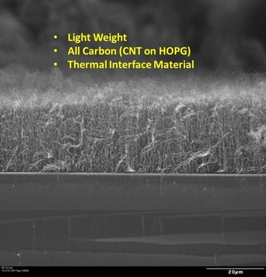
More details of CNT growth, such as number of nanotubes per unit area of substrate, and their length (carpet height) can be obtained from their SEM images. The CNT growth density can be estimated using the SEM image depth of field and count the number of CNTs visible in an image area. In this study, the number of CNTs was measured to be 77 ± 6 CNTs/µm2 or 7.7 × 10⁹ CNTs/cm2. Several studies have attempted to measure CNT density in arrays grown on different types of substrates using different deposition techniques [7,27,28], which show a wide range from about 8 × 10⁹ to 5 × 10¹¹ CNTs/cm2. It must be pointed out that this is an estimate only, and there is a possibility of underestimating the total number of CNT in a given area because a SEM image can only capture objects within the line of sight, and this can lead to some unaccounted CNTs that fall outside of the field of view or are hidden behind a visible CNT. Secondly, it is assumed that the number of CNTs stays the same from the interface of the sample to the CNT tips. This may not be true, since it is possible for new CNTs to grow some distance away from the interface. Therefore, using SEM to estimate the number of CNTs leads to a number that represents minimum numbers of CNTs in an area.
Each component within the thermal interface can affect the thermal pathway, and thereby increase the overall thermal resistance. Therefore, it is important to examine the interface to determine if any obstructions are in the thermal pathway. Figure 2 is a set of TEM images taken from the CNT/HOPG interface. The inset in Figure 2b is an SEM image prior to the TEM alteration and shows that the CNTs used for thermal measurements were uniform and aligned before FIB processing. Figure 2e is a merged image that shows the location of the Fe catalyst particles in relation to the oxide at the interface. In theory, the particles should have some thermal resistance contributions; however due to their size being small in scale (10 nm), it is expected that the contribution would be small as well. Hence, these particles were not treated as a separate component/layer in the thermal analysis portion of this study.
3.2. Thermal Analysis
The LFA system uses a laser pulse to deposit energy on the front face of a sample, and a detector measures the temperature response of the rear face. LFA uses validated models from literature to determine the thermal diffusivity, α, of the sample or layer in question. Once the diffusivity is determined, both the thermal conductivity (κ), and the thermal resistance (R), can be calculated. To calculate the thermal conductivity of the sample, Equation (2) can be used
where ρ (g/cm3) and (J/g °C) are density and specific heat, respectively. The specific heat (cp) for the samples were measured using differential scanning calorimetry (DSC). Small carbon samples were measured against an empty platinum dish to obtain the average Cp values used in the study. To determine the thermal resistance value (R), Equation (3) is used
where is the thickness of the thermal layer within the sample.
3.2.1. Thermal Analysis of the Substrate (HOPG)
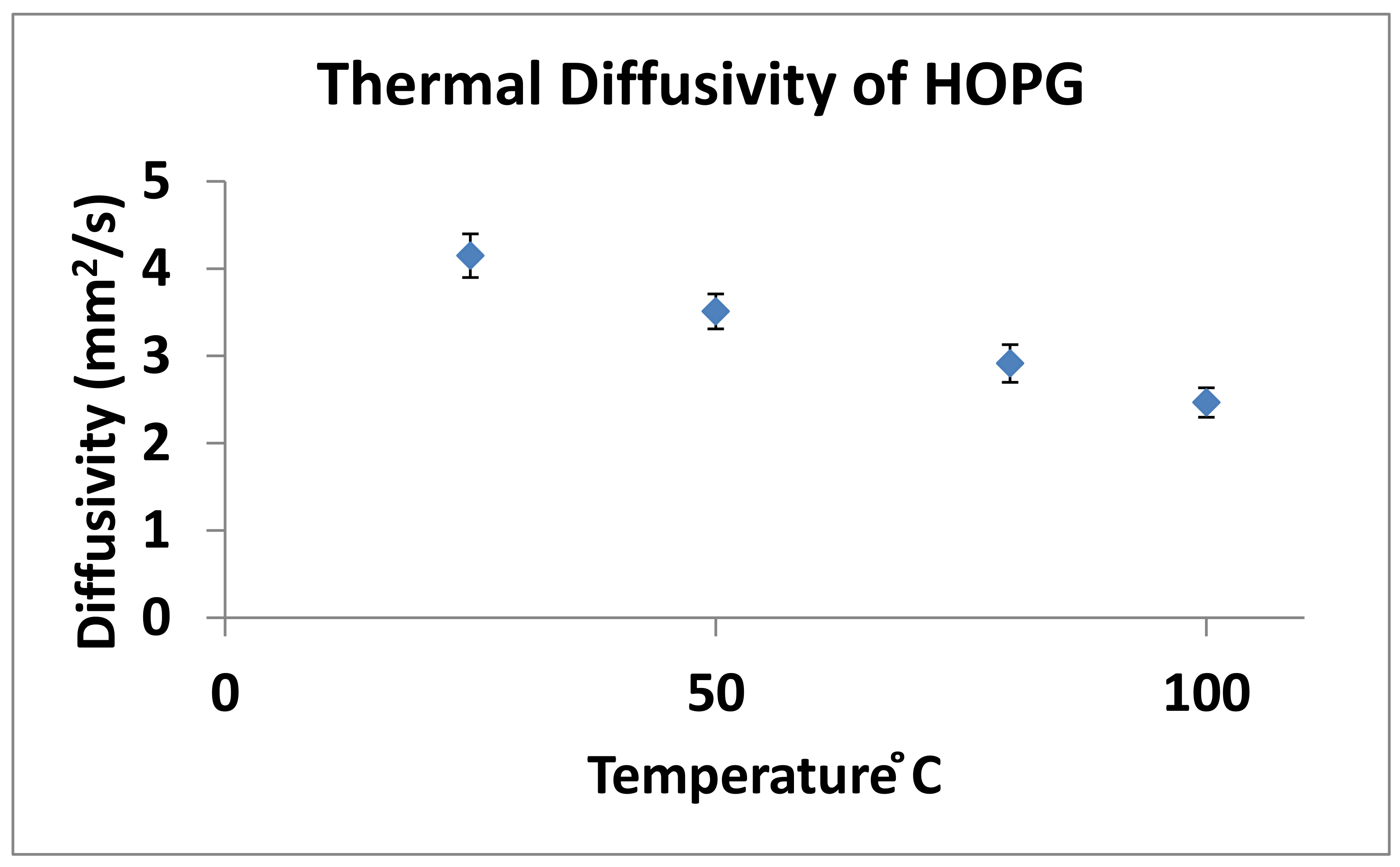
The HOPG sample is an excellent sample to be measured by the LFA system because it is made of graphite and nontransparent to the IR detector. Figure 3 shows the average thermal diffusivity values of HOPG samples measured over the temperature range of (25–100 °C).
3.2.2. Thermal Analysis of Substrates with a Buffer Layer
Diffusivity values were obtained for HOPG samples coated with a SiO2 buffer layer. It was determined that the oxide layer was too thin for the LFA system to measure the diffusivity contributions. Namely, the measured diffusivity value for the SiO2-coated HOPG samples were essentially the same as those measured of the baseline HOPG sample, Figure 3. Using a referenced thermal conductivity value for silica, 1.4 W/m-K, the thermal resistance of the silica oxide layer was estimated. It shows that the thermal resistance value for the silica buffer layer is indeed expected to be several orders of magnitude smaller, 5.21 × 10⁻⁸ m2K/W, than that of the HOPG substrate layer ~2.5 × 10⁻⁴ m2K/W. Therefore, it is safe to assume that the oxide buffer layer has negligible thermal resistance contribution, as indicated in Table 2.
3.2.3. Thermal Analysis of Substrates with a Buffer Layer and CNT Array Film
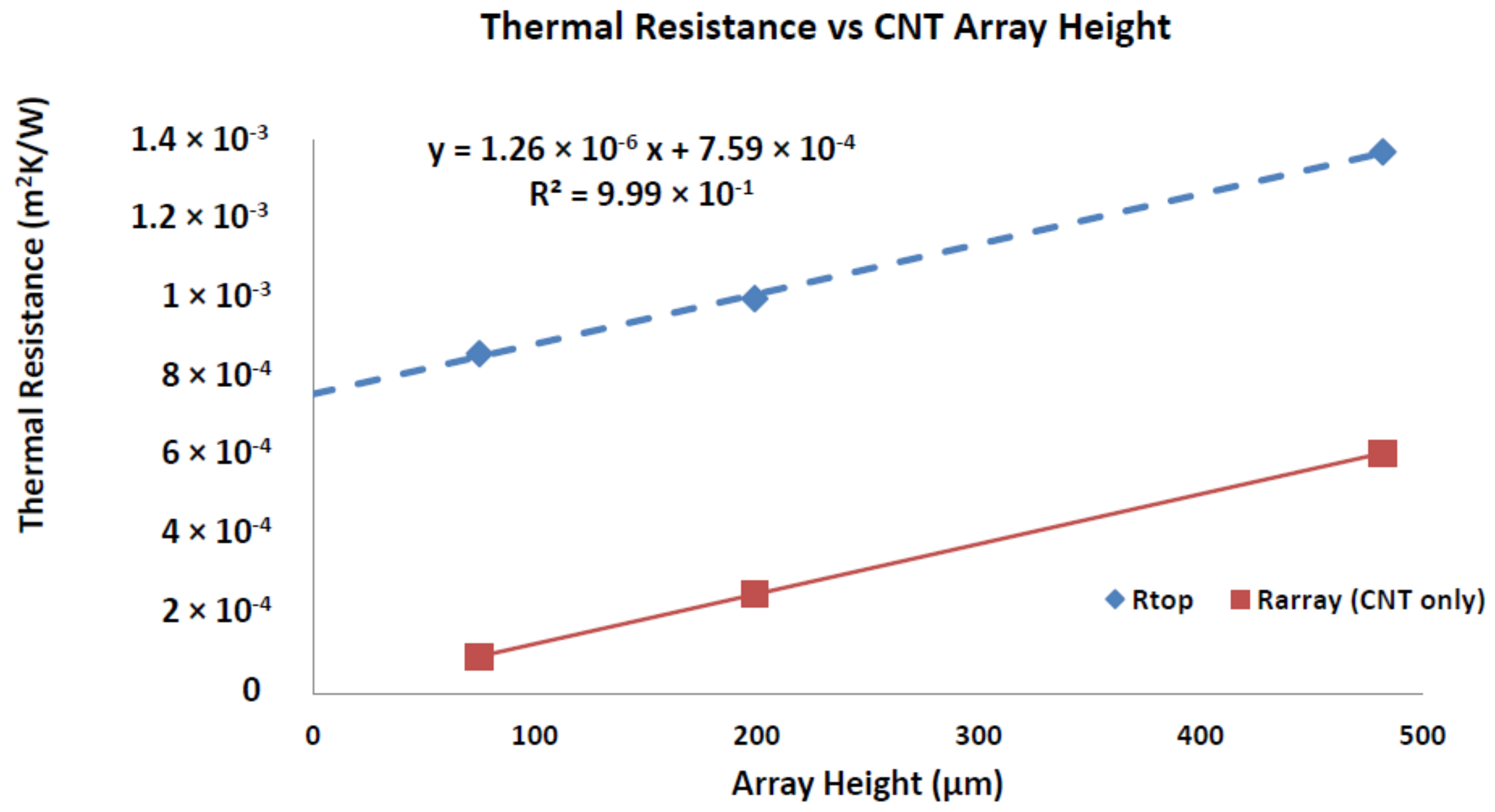
In this investigation, CNT arrays were grown as a uniform film on the oxide-coated HOPG samples. The oxide-coated HOPG substrate was considered the bottom layer of the composite, and the CNT film and the corresponding Rinterface were treated as the top layer. The previously obtained thermal diffusivity value and corresponding physical properties of the bottom layer of each sample (HOPG 1, 2 and 3) was first entered as a known value in the Netzsch LFA two-layer analysis. The resulting average diffusivity values for the top layer of each sample (CNT I (482 µm), II (199 µm), and III (75 µm)) are listed in Table 2. The thermal diffusivity value for the top layer was converted to thermal resistance, using Equations (2) and (3), to compare the thermal resistance contributions from each of the layers.
In Figure 4, Rtop is plotted and it is the value for the sum of CNT array and the Rinterface. It can be seen that there is a linear trend between Rarray and the height of the CNT arrays. Since all the samples use the same growth parameters (other than growth time), it was assumed that the CNT/HOPG interface resistance, Rinterface, for all samples were the same. Therefore, the contribution of Rinterface to the combined resistance of Rtop can be obtained by a linear line extrapolated to the y-axis intercept. Based on this y-intercept, Rinterface is estimated to be 7.59 × 10⁻⁴ m2 K/W. Rarray values for each of the three samples were calculated by subtracting Rinterface from the respective Rtop values. The thermal conductivity value of the CNT array was then calculated to be 7.91 × 10⁻¹ W/m-K, from the inverse of the slope of the trend line.
3.2.4. CNT Thermal Conductivity Analysis
Using the array thermal conductivity calculated above, it is also possible to calculate the thermal conductivity value of a single CNT (κCNT). To accomplish this, an equation was formulated using simplified assumptions about the CNT array. It was assumed that all individual CNTs in the array are solid cylinders and they are all uniform in material composition (morphology, tube diameter, and height). In addition, the CNTs are in parallel with each other and occupy a certain volume fraction, 8.5% in this case. Furthermore, the thermal conductivity values of each CNT in the array are equal and are constant along the length of CNT, Figure 5. If the number of CNTs per area and the diameter of the CNT are known, then the thermal conductivity value of a CNT, κCNT, can be calculated using Equation (4).
where d is the average diameter of the CNTs and N is the number of CNTs per area.
Using the SEM images, the average CNT diameter was measured to be 19 ± 5 nm, and the growth density was measured to be 7.7 ± 0.6 × 10¹³ CNTs/m2. Using Equation (4), the thermal conductivity of a CNT, κCNT, was calculated to be 35.09 W/m-K. Note that this is the average thermal conductivity of the CNT assuming the CNT to be a solid cylinder. While this is not the highest thermal conductivity value reported for carbon nanotubes, it is an excellent value. As discussed in the introduction, the reported thermal conductivity of CNT ranges from 0.145–3000 W/m-K depending on the quality of CNT, sample configuration and testing methods. From the engineering point of view, 35 W/m-K is superior to many commercially available thermal interface materials (thermal grease, or epoxy bond, etc.) used today. Unlike many examples shown previously were the CNT arrays were created on silicon substrates, here the combination of CNTs on HOPG shows promise as a new TIM for certain electronic applications. This value shows the possibility of using samples in such configuration (aligned and attached CNTs on HOPG) as new TIM for certain electronic applications. The region of concern, that is actually showing relatively high thermal resistance in these samples, is actually the interface region (Rinterface estimated to be about 7.59 × 10⁻⁴ m2 K/W as shown in the last section). It is possible that earlier studies that estimate lower values of Rinterface may be doing so because they are assuming lower thermal conductivity of nanotubes. In this study, it was possible to decouple the contribution from the two regions. These results indicate that, when robust durable CNT arrays are attached on graphite, the interfacial zone may be become the bottleneck for thermal transport and will need to be improved or minimized or future improvements in these materials.
3.2.5. Thermal Resistance Analytical Model
Equation (5) (parameter sensitivity analysis) was created, by rearranging Equation (4), to help to predict the effect of CNT morphology and growth density on thermal resistivity of the array.
Figure 6, shows that if the number of CNTs per given area is increased, Rarray would decrease, as expected. However, there is a limitation on how much improvement can be achieved, since Rarray convenes to an asymptote. This suggests that once a critical CNT growth density is reached, any additional increases do not greatly improve the thermal resistance. The result also shows that the effect of CNT length diminishes as the density of CNT increases, suggesting that CNT growth density is the dominant factor affecting the thermal resistance. There will also be a practical limit set by the density at which the individual nanotubes touch each other and cannot be grown any closer together. This simple model underscores that through CNT growth optimization, the thermal resistance of the array can be further reduced. Using the thermal conductivity value of 35 W/m-K, the best possible thermal resistance achievable will be about 2 × 10⁻⁶, if pristine samples of CNT with 100% growth coverage were fabricated. This value places samples in this configuration (CNTs grown on HOPG substrate) on par with many commercially available TIM samples. However, it must be noted that while such all-carbon hierarchical structure shows promise for thermal applications additional research will be needed to finally integrate these materials with specific thermal devices having minimal CTE mismatch, compatible interface, and higher thermal conductivity that can operate in conditions involving different functional requirements and cooling environment.
4. Concluding Remarks
In this investigation, carpet-like arrays of carbon nanotubes (CNT) were attached to oxide-coated HOPG substrates, and direct bonding between CNT and the oxide layer was achieved at the interface. It was shown by high-resolution TEM images that the catalyst particles were imbedded in the oxide layer. Using the height of CNT array as the variable, the thermal properties of all these carbon samples were determined. The result shows that Rarray is linearly related to the CNT array height. It was also calculated that the thermal conductivity value for a CNT was about 35 W/m-K. Furthermore, this investigation provided a simple analytical model to determine the effect of different CNT variables on thermal resistance. The model suggests that if pristine CNT with maximum packing density can be achieved, an optimally low thermal resistance value of about 2 × 10⁻⁶ m2 K/W is obtainable in the array. This value placed the thermal resistance of CNT in such a configuration (CNT on HOPG), on par with current commercially available TIM material, with the added benefit of all carbon systems being that it is strong, durable, compliant and will not suffer from drying out or thermal cycling issues.
Author Contributions
For research articles with several authors, a short paragraph specifying their individual contributions must be provided. B.T.Q. and L.E. conceived and designed the experiments; B.T.Q. performed the experiments; B.T.Q., L.E., J.D.S. and S.M.M. analyzed the data; J.D.S. and S.M.M. provided mentorship and guidance on the experiment; B.T.Q. and S.M.M. wrote the paper, L.E. and J.D.S. provided editorial expertise.
Acknowledgments
Financial support from the National Science Foundation NSF-CBET (1747826) is acknowledged. The facilities used were funded by the NSF-MRI award and Ohio Board of Regents. The authors are grateful to S. Ganguli for useful discussions prior to experimental set-up.
Conflicts of Interest
The authors declare no conflict of interest.
References
- Incropera, F.P.; DeWitt, D.P. Fundamental of Heat and Mass Transfer, 5th ed.; John Wiley & Sons: New York, NY, USA, 2002. [Google Scholar]
- Ganguli, S.; Roy, A.K.; Wheeler, R.; Varshney, V.; Du, F.; Dai, L. Superior thermal interface via vertically aligned carbon nanotubes grown on graphite foils. J. Mater. Res. 2012, 28, 933–939. [Google Scholar] [CrossRef]
- Sarvar, F.; Whalley, D.; Conway, P. Thermal Interface Materials—A Review of the State of the Art. In Proceedings of the 2006 1st Electronic Systemintegration Technology Conference, Dresden, Germany, 5–7 September 2006; Volume 2, pp. 1292–1302. [Google Scholar]
- Balandin, A. Thermal Properties of graphene and nanostructured carbon material. Nat. Mater. 2011, 10, 569–581. [Google Scholar] [CrossRef] [PubMed]
- Renteria, J.D.; Nika, D.L.; Balandin, A.A. Graphene thermal Properties: Applications in Thermal Management and Energy Storage. Appl. Sci. 2014, 4, 525–547. [Google Scholar] [CrossRef]
- Nika, D.L.; Balanddin, A. Phonons and thermal transport in graphene and graphene-based materials. Rep. Prog. Phys. 2017, 80, 036502. [Google Scholar] [CrossRef] [PubMed]
- Sun, D.; Timmermans, M.Y.; Tian, Y.; Nasibulin, A.G.; Kauppinen, E.I.; Kishimoto, S.; Mizutani, T.; Ohno, Y. Flexible high-performance carbon nanotube integrated circuits. Nat. Nanotechnol. 2011, 6, 156–161. [Google Scholar] [CrossRef] [PubMed]
- Cao, Q.; Kim, H.; Pimparkar, N.; Kulkarni, J.P.; Wang, C.; Shim, M.; Roy, K.; Alam, M.A.; Rogers, J.A. Medium-scale carbon nanotube thin-film integrated circuits on flexible plastic substrates. Nature 2008, 454, 495–500. [Google Scholar] [CrossRef] [PubMed]
- Prestes, E.; Souza, T.; Pandolfelli, V.; Gomes, D. Thermal Expansion Mismatch Analysis of Nano-bonded Refractory Castables. Int. J. Appl. Ceram. Technol. 2014, 11, 984–992. [Google Scholar] [CrossRef]
- Prieto, R.; Molina, J.M.; Narciso, J.; Louis, E. Fabrication and properties of graphite flakes/metal composites for thermal management applications. Scr. Mater. 2008, 59, 11–14. [Google Scholar] [CrossRef]
- Molina, J.M.; Narciso, J.; Weber, L.; Mortensen, A.; Louis, E. Thermal conductivity of Al-SiC composites with monomodal and bimodal particle size distribution. Mater. Sci. Eng. A 2008, 480, 483–488. [Google Scholar] [CrossRef]
- Molina, J.M.; Rodríguez-Guerrero, A.; Louis, E.; Rodríguez-Reinoso, F.; Narciso, J. Porosity effect on thermal properties of Al-12 wt % Si/graphite composites. Materials (Basel) 2017, 10, 177. [Google Scholar] [CrossRef] [PubMed]
- Malekpour, H.; Chang, K.H.; Chen, J.C.; Lu, C.Y.; Nika, D.L.; Novoselov, K.S.; Balandin, A.A. Thermal conductivity of graphene laminate. Nano Lett. 2014, 14, 5155–5161. [Google Scholar] [CrossRef] [PubMed]
- Renteria, J.D.; Ramirez, S.; Malekpour, H.; Alonso, B.; Centeno, A.; Zurutuza, A.; Cocemasov, A.I.; Nika, D.L.; Balandin, A.A. Strongly Anisotropic Thermal Conductivity of Free-Standing Reduced Graphene Oxide Films Annealed at High Temperature. Adv. Funct. Mater. 2015, 25, 4664–4672. [Google Scholar] [CrossRef]
- Gulotty, R.; Castellino, M.; Jagdale, P.; Tagliaferro, A.; Balandin, A.A. Effects of functionalization on thermal properties of single-wall and multi-wall carbon nanotube-polymer nanocomposites. ACS Nano 2013, 7, 5114–5121. [Google Scholar] [CrossRef] [PubMed]
- Renteria, J.; Legedza, S.; Salgado, R.; Balandin, M.P.; Ramirez, S.; Saadah, M.; Kargar, F.; Balandin, A.A. Magnetically-functionalized self-aligning graphene fillers for high-efficiency thermal management applications. Mater. Des. 2015, 88, 214–221. [Google Scholar] [CrossRef]
- Berber, S.; Kwon, Y.; Tomanek, D. Unusually high thermal conductivity of carbon nanotubes. Phys. Rev. Lett. 2000, 84, 4613. [Google Scholar] [CrossRef] [PubMed]
- Akoshima, M.; Hata, K.; Futaba, D.N.; Mizuno, K.; Baba, T.; Yumura, M. Thermal diffusivity of single-walled carbon nanotube forest measured by laser flash method. Jpn. J. Appl. Phys. 2009, 48, 05EC07. [Google Scholar] [CrossRef]
- Hone, J.; Whitney, M.; Piskoti, C.; Zettl, A. Thermal conductivity of single-walled carbon nanotubes. Phys. Rev. B 1999, 59, R2514–R2516. [Google Scholar] [CrossRef]
- Hone, J. Carbon Nanotubes: Thermal Properties. In Dekker Encyclopedia of Nanoscience and Nanotechnology; CRC Press: Boca Raton, FL, USA, 2004; pp. 603–611. [Google Scholar]
- Sato, K.; Shiraiwa, T.; Maruyama, T.; Naritsuka, S. Effect of buffer thickness on single-walled Carbon Nanotube Growth Using Aluminum Oxide Buffer Layer with Alcohol Gas Source Method. J. Nanosci. Nanotechnol. 2010, 10, 3929–3933. [Google Scholar] [CrossRef] [PubMed]
- Ma, W.; Miao, T.; Zhang, X.; Yang, L.; Cai, A.; Yong, Z.; Li, Q. Thermal performance of vertically-aligned multi-walled carbon nanotube array grown on platinum film. Carbon 2014, 77, 266–274. [Google Scholar] [CrossRef]
- Fujii, M.; Zhang, X.; Xie, H.; Ago, H.; Takahashi, K.; Ikuta, T.; Abe, H.; Shimizu, T. Measuring the Thermal Conductivity of a Single Carbon Nanotube. Phys. Rev. Lett. 2005, 95, 65502. [Google Scholar] [CrossRef] [PubMed]
- Yu, C.; Shi, L.; Yao, Z.; Li, D.; Majumdar, A. Thermal conductance and thermopower of an individual single-wall carbon nanotube. Nano Lett. 2005, 5, 1842–1846. [Google Scholar] [CrossRef] [PubMed]
- Kim, P.; Shi, L.; Majumdar, A.; McEuen, P.L. Thermal Transport Measurements of Individual Multiwalled Nanotubes. Phys. Rev. Lett. 2001, 87, 215502. [Google Scholar] [CrossRef] [PubMed]
- Li, Q.; Liu, C.; Wang, X.; Fan, S. Measuring the thermal conductivity of individual carbon nanotubes by the Raman shift method. Nanotechnology 2009, 20, 145702. [Google Scholar] [CrossRef] [PubMed]
- Yang, D.J.; Zhang, Q.; Chen, G.; Yoon, S.F.; Ahn, J.; Wang, S.G.; Zhou, Q.; Wang, Q.; Li, J.Q. Thermal conductivity of multiwalled carbon nanotubes. Phys. Rev. B 2002, 66, 165440. [Google Scholar] [CrossRef]
- Ivanov, I.; Puretzky, A.; Eres, G.; Wang, H.; Pan, Z.; Cui, H.; Jin, R.; Howe, J.; Geohegan, D.B. Fast and highly anisotropic thermal transport through vertically aligned carbon nanotube arrays. Appl. Phys. Lett. 2006, 89, 174–177. [Google Scholar] [CrossRef]
- Hu, M.; Keblinski, P.; Wang, J.-S.; Raravikar, N. Interfacial thermal conductance between silicon and a vertical carbon nanotube. J. Appl. Phys. 2008, 104, 83503. [Google Scholar] [CrossRef]
- Lin, W.; Shang, J.; Gu, W.; Wong, C.P. Parametric study of intrinsic thermal transport in vertically aligned multi-walled carbon nanotubes using a laser flash technique. Carbon 2012, 50, 1591–1603. [Google Scholar] [CrossRef]
- Wang, X.; Zhong, Z.; Xu, J. Noncontact thermal characterization of multiwall carbon nanotubes. J. Appl. Phys. 2005, 97, 064302. [Google Scholar] [CrossRef]
- Shaikh, S.; Li, L.; Lafdi, K.; Huie, J. Thermal conductivity of an aligned carbon nanotube array. Carbon 2007, 45, 2608–2613. [Google Scholar] [CrossRef]
- Mukhopadhyay, S.M.; Karumuri, A.; Barney, I.T. Hierarchical nanostructures by nanotube grafting on porous cellular surfaces. J. Phys. D Appl. Phys. 2009, 42, 195503. [Google Scholar] [CrossRef]
- Barney, I.T.; Ganguli, S.; Roy, A.K.; Mukhopadhyay, S.M. Improved Thermal Response in Encapsullated Phase change materials by nanotube Attachment on Encapsulating Solid. J. Nanotechnol. Eng. Med. 2012, 3, 031005. [Google Scholar] [CrossRef]
- Quinton, B.T.; Leedy, K.D.; Lawson, J.W.; Tsao, B.; Scofield, J.D.; Merrett, J.N.; Zhang, Q.; Yost, K.; Mukhopadhyay, S.M. Influence of oxide buffer layers on the growth of carbon nanotube arrays on carbon substrates. Carbon 2015, 87, 175–185. [Google Scholar] [CrossRef]
- Pulikollu, R.V. Nano-Coatings on Carbon Structures for Interfacial Modification. Ph.D. Dissertation, Wright State University, Dayton, OH, USA, 2005. [Google Scholar]
- Parker, W.J.; Jenkins, R.J.; Butler, C.P.; Abbott, G.L. Flash method of determining thermal diffusivity, heat capacity, and thermal conductivity. J. Appl. Phys. 1961, 32, 1679–1684. [Google Scholar] [CrossRef]
Figure 1.
(a) Cartoon representation of the sample for a 2-layer thermal analysis model, (b) is a 3-D cartoon representation of the sample. Note: Figures are not drawn to scale.
Figure 1.
(a) Cartoon representation of the sample for a 2-layer thermal analysis model, (b) is a 3-D cartoon representation of the sample. Note: Figures are not drawn to scale.

Figure 2.
SEM and TEM images of the CNT/HOPG interface, the TEM uses EELS technique to find the oxide layer and the iron catalyst particles. (a) SEM image of the lifted cross-section foil of the sample; (b) cross-section SEM image of the grown sample, with high magnification image as the small insert to the top left; (c) TEM image of the sample taken at the CNT/HOPG interface; (d) EELS scan for elemental Si, over the area shown in figure (c); (e) Merged image from figures (d, f); (f) EELS scan for elemental Fe, over the area shown in figure (c).

Figure 3.
Diffusivity values for uncoated HOPG samples and samples painted with graphite.

Figure 4.
Thermal Resistance of samples with different CNT height.

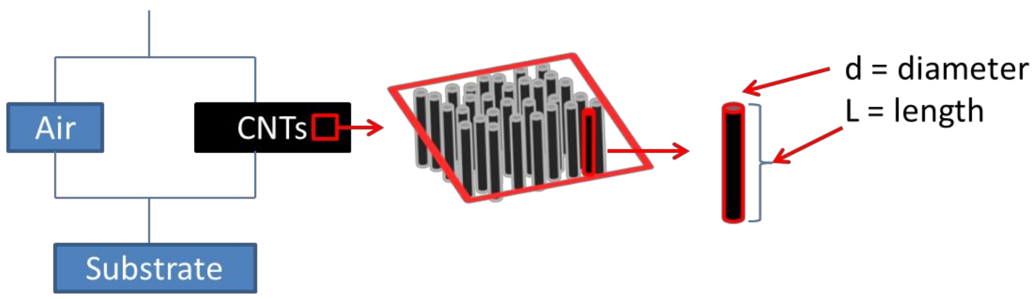
Figure 5.
Modeling CNT array in parallel with air and image of simplified CNT.

Figure 6.
Shows how the variable (Number of CNT/area) would change thermal resistance using the model equation. The experimental values are marked in each of the lines.
Figure 6.
Shows how the variable (Number of CNT/area) would change thermal resistance using the model equation. The experimental values are marked in each of the lines.


Table 1.
Sample properties.
| Bottom Layer Samples | Cap | Top Layer Samples | |||||
|---|---|---|---|---|---|---|---|
| Units | HOPG 1 | HOPG 2 | HOPG 3 | HOPG Cap | CNT I (482 μm) | CNT II (199 μm) | CNT III (75 μm) |
| mm | 10 mm × 10 mm (nominal sample Size) | ||||||
| mm | 1.23 ± 0.01 | 1.37 ± 0.01 | 1.42 ± 0.01 | 1.15 ± 0.01 | 0.482 ± 8 × 10⁻⁴ | 0.199 ± 7 × 10⁻⁴ | 0.075 ± 6 × 10⁻⁴ |
| g | 0.2518 | 0.306 | 0.3148 | 0.2363 | 4.2 × 10⁻³ | 2.1 × 10⁻³ | 1.90 × 10⁻³ |
| g/cm3 | 2.16 ± 0.01 | 0.091 | 0.102 | 0.248 | |||
Table 2.
Thermal Analysis Results.
| Bottom Layer Samples | Top Layer Samples | ||||||
|---|---|---|---|---|---|---|---|
| Units | HOPG 1 | HOPG 2 | HOPG 3 | CNT I (482 μm) | CNT II (199 μm) | CNT III (75 μm) | |
| α | mm2/s | 3.864 ± 0.06 | 4.053 ± 0.08 | 4.177 ± 0.09 | 6.099 ± 0.04 | 3.088 ± 0.04 | 0.558 ± 0.03 |
| Cp | J/(g × K) | 0.63 ± 0.01 | |||||
| κ | W/mK | 5.23 | 5.52 | 5.71 | 0.351 | 0.199 | 0.087 |
| Rbottom = Rsub + Roxide | m2 K/W | 2.35 × 10⁻⁴ | 2.48 × 10⁻⁴ | 2.49 × 10⁻⁴ | - | ||
| Roxide | m2 K/W | 5.21 × 10⁻⁸ | |||||
| Rtop = Rarray + Rinterface | m2 K/W | - | 1.37 × 10⁻³ | 1 × 10⁻³ | 8.61 × 10⁻⁴ | ||
| Rinterface (Figure 5) | m2 K/W | 7.59 × 10⁻⁴ | |||||
| κarray (Figure 5) | m2 K/W | 7.91 × 10⁻¹ | |||||
| Rarray | m2 K/W | 6.09 × 10⁻⁴ | 2.52 × 10⁻⁴ | 9.48 × 10⁻⁵ | |||
© 2018 by the authors. Licensee MDPI, Basel, Switzerland. This article is an open access article distributed under the terms and conditions of the Creative Commons Attribution (CC BY) license (http://creativecommons.org/licenses/by/4.0/).
Share and Cite
MDPI and ACS Style
Quinton, B.T.; Elston, L.; Scofield, J.D.; Mukhopadhyay, S.M. Aligned Carbon Nanotube Arrays Bonded to Solid Graphite Substrates: Thermal Analysis for Future Device Cooling Applications. C 2018, 4, 28. https://doi.org/10.3390/c4020028
AMA Style
Quinton BT, Elston L, Scofield JD, Mukhopadhyay SM. Aligned Carbon Nanotube Arrays Bonded to Solid Graphite Substrates: Thermal Analysis for Future Device Cooling Applications. C. 2018; 4(2):28. https://doi.org/10.3390/c4020028
Chicago/Turabian StyleQuinton, Betty T., Levi Elston, James D. Scofield, and Sharmila M. Mukhopadhyay. 2018. "Aligned Carbon Nanotube Arrays Bonded to Solid Graphite Substrates: Thermal Analysis for Future Device Cooling Applications" C 4, no. 2: 28. https://doi.org/10.3390/c4020028
Note that from the first issue of 2016, this journal uses article numbers instead of page numbers. See further details here.