Article

Raman Study of Polycrystalline Si3N4 Irradiated with Swift Heavy Ions

by
Ainash Zhumazhanova
1,2,
Alisher Mutali
1,2,3,
Anel Ibrayeva
1,2,3,
Vladimir Skuratov
3,4,5,
Alma Dauletbekova
1,*,
Ekaterina Korneeva
3,
Abdirash Akilbekov
1 and
Maxim Zdorovets
1,2,6
1
Department of Technical Physics, L.N. Gumilyov Eurasian National University, Nur-Sultan 010008, Kazakhstan
2
Astana Branch of the Institute of Nuclear Physics, Nur-Sultan 010000, Kazakhstan
3
G.N. Flerov Laboratory of Nuclear Reactions, Joint Institute for Nuclear Research, 141980 Dubna, Russia
4
Institute of Nuclear Physics and Engineering, National Research Nuclear University «MEPhI», 115409 Moscow, Russia
5
Department of Nuclear Physics, University «Dubna», 141982 Dubna, Russia
6
Ural Federal University, 620002 Yekaterinburg, Russia
*
Author to whom correspondence should be addressed.
Crystals 2021, 11(11), 1313; https://doi.org/10.3390/cryst11111313
Submission received: 12 September 2021 / Revised: 25 October 2021 / Accepted: 26 October 2021 / Published: 28 October 2021
(This article belongs to the Section Polycrystalline Ceramics)

Abstract

:
A depth-resolved Raman spectroscopy technique was used to study the residual stress profiles in polycrystalline silicon nitride that was irradiated with Xe (167 MeV, 1 × 1011 cm−2 ÷ 4.87 × 1013 cm−2) and Bi (710 MeV, 1 × 1011 cm−2 ÷ 1 × 1013 cm−2) ions. It was shown that both the compressive and tensile stress fields were formed in the irradiated specimen, separated by a buffer zone that was located at a depth that coincided with the thickness of layer, amorphized due to multiple overlapping track regions. The compressive stresses were registered in a subsurface region, while at a greater depth, the tensile stresses were recorded and their levels reached the maximum value at the end of ion range. The size of the amorphous layer was evaluated from the dose dependence of the full width at half maximum (FWHM) (FWHM of the dominant 204 cm−1 line in the Raman spectra and scanning electron microscopy.

Graphical Abstract

1. Introduction

Irradiation with heavy ions of 1–3 MeV/nucleon energies is characterized by pronounced inhomogeneous ionization and nuclear stopping profiles. As a result, the level of energy losses varies over a very wide range, which, in turn, leads to an inhomogeneous spatial distribution of the radiation damage and the associated mechanical stresses. The range of ions with the above energies, depending on the density of the material, does not exceed several tens of microns. For energies of ~1 MeV/nucleon, which are of the greatest interest from a practical point of view for the simulation of the fission fragments impact, this value is in the range of several microns to ~10 microns. Therefore, to get reliable information about the stress profiles, it is necessary to use experimental methods with a spatial resolution of ~1 micron. Such accuracy can be achieved in techniques that are based on the use of the piezospectroscopic effect (PS), which connects the spectral shift in optical absorption, luminescence, or Raman scattering spectra with the level of mechanical stresses [1,2].
The physical nature of the PS effect is based on the fact that when the lattice of ions that are surrounding an optically active impurity or defect is distorted, for example, under the action of applied stresses, the potential of the crystal field in the luminescent site changes, which changes the energies of electronic transitions (i.e., any applied or residual stress induces changes in the vibrational and electronic levels of the studied material). Although the Raman signal is directly sensitive to strain rather than stress, conversion to stress is easy if the corresponding elastic constants are known. When they are unknown, the problem can be circumvented by performing piezospectroscopic calibration on the same material [1,2]. In the linear approximation, the piezospectroscopic effect (PS) is expressed as a Taylor’s expansion about the unperturbed (i.e., unstressed) center peak position of the frequency ν 0 :
ν σ = ν 0 + ( ν σ i j ) i j σ i j ,
Equation (1) shows that the stress induced shift, Δ ν = ν σ ν 0 , a scalar quantity, is the product of the stress tensor, σ i j , times the tensor of the first derivatives, which is called the piezospectroscopic tensor and is usually denoted as Π i j and is usually represented as:
Δ ν = Π i j σ i j ,
As noted above, the piezospectroscopic coefficients are determined by means of appropriate calibrations, during which a known stress is applied to the material and the corresponding change in the frequency relative to the unstressed state is recorded [1,2].
It should also be emphasized that the PS effect does not depend on the source of the spectral signal: photoluminescence, cathodoluminescence, or Raman scattering. In other words, regardless of whether monochromatic light, electrons, or ions are used as radiation sources to stimulate luminescence, we can track the emission wavelength/frequency shift in spectral lines to obtain voltage information [2]. For example, photoluminescence experiments are characterized by high sensitivity, but their significant drawback is the limited number of transparent materials for which they can be applied, for example, Al2O3:Cr (ruby), borosilicate glasses with Sm3+ impurities. To date, the most studied are the piezospectroscopic properties of fluorescence due to Cr+3 ions in the structure of Al2O3 single crystals [3,4], which is used to measure pressure in diamond anvils [5] and in polycrystalline aluminum oxide [6]. In [7,8,9,10], the registration of the ion and photoluminescence spectra of Cr+3 was used to obtain data on the mechanical stresses in ruby during and after irradiation with high-energy heavy ions.
The PS effect that was based on the analysis of Raman spectra is characterized by a lower intensity of spectral lines and, therefore, lower sensitivity compared to luminescence, but it can provide information on the structure and mechanical stresses, and also allows one to study radiation-resistant insulators, including ceramics, such as the object of this work—polycrystalline silicon nitride Si3N4 [11].
It is known that Si3N4 is the only nitride ceramic in which latent tracks of fast heavy ions have been found [12,13,14,15,16,17,18,19,20,21]. They are extended structural defects that are formed due to high-density ionization that cannot be reproduced under other types of radiation exposure. One of the consequences of the formation of latent tracks are local mechanical stresses in the region of the ion trajectory. Therefore, the parameters of the stress field, the level, and the spatial distribution will be determined by the density of such regions and their interference during overlap (especially multiple), which occurs already at fluences ~1 × 1013 cm−2. At present, such processes remain practically unexplored. The aim of this work is to study the structural state and profiles of mechanical stresses over the depth of a layer of polycrystalline silicon nitride β-Si3N4 that has been irradiated with high-energy xenon (Xe) and bismuth (Bi) ions by Raman spectroscopy methods.

2. Experimental Details

Materials and Methods

The objects of study of this work were polycrystalline samples of silicon nitride β-Si3N4, manufactured by MTI Corporation, with grain sizes that range from several hundred nanometers to several microns. According to the data of energy-dispersive analysis, an aluminum impurity was detected in the composition of Si3N4 in an amount of ~3 at. %, At the same time, the aluminum concentration in some grains was at an undetectable level.
The samples were irradiated with 167 MeV 132Xe and with 710 MeV 209Bi ions with at room temperature at the IC-100 and U-400 FLNR JINR cyclotrons (Dubna, Russia), respectively. The irradiation parameters of energy, fluence and electronic stopping power at the target surface (Se), and the projective range (Rp) were calculated using SRIM code [22] are given in Table 1.
The Raman spectra from irradiated samples were measured a using Solver Specrtum, NT-MDT laser confocal scanning microscope. The spectra were excited at a wavelength λ = 473 nm and were recorded by scanning both the surface and the polishing edge of the sample across the ion trajectory. The size of the laser spot and scanning step were 1 μm and 0.25 μm, respectively. The measurement time that was optimized for maximum intensity and was 30 s. Usually, we began scanning at a distance of approximately 1 µm from the surface. Scanning electron microscopy (SEM) analysis of samples was carried out using Hitachi S-3400N SEM in secondary electrons at an accelerating voltage of 10 kV.

3. Results and Discussion
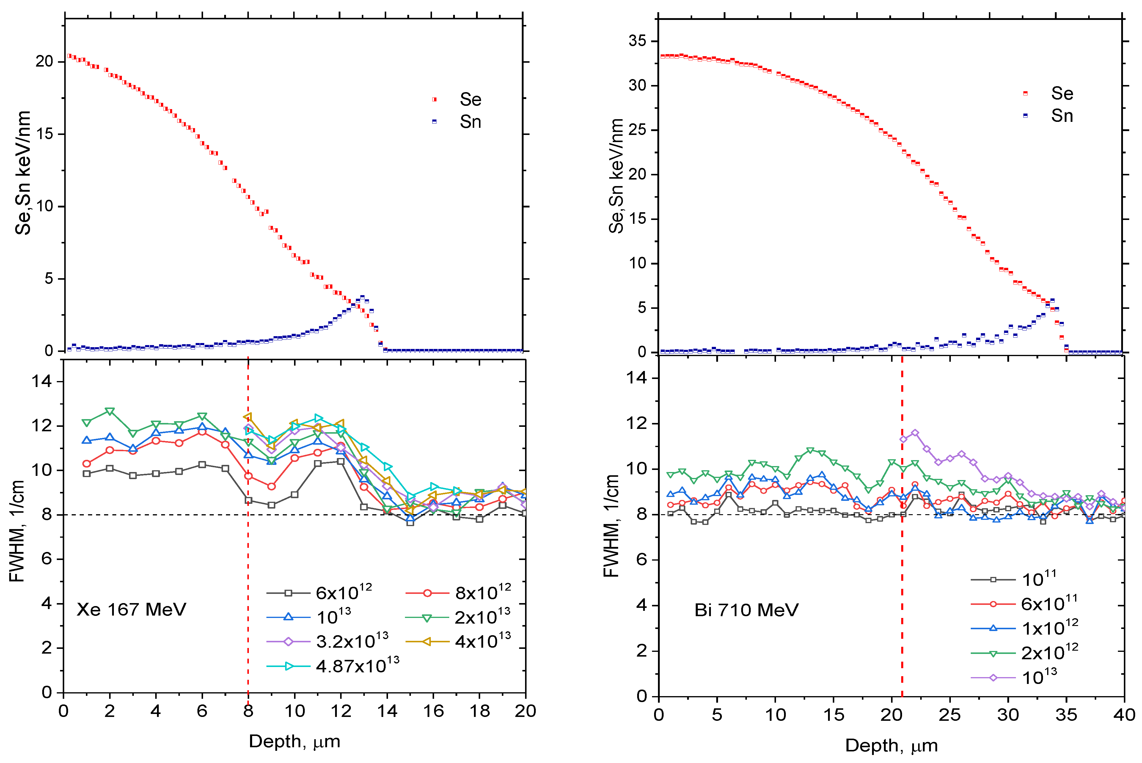
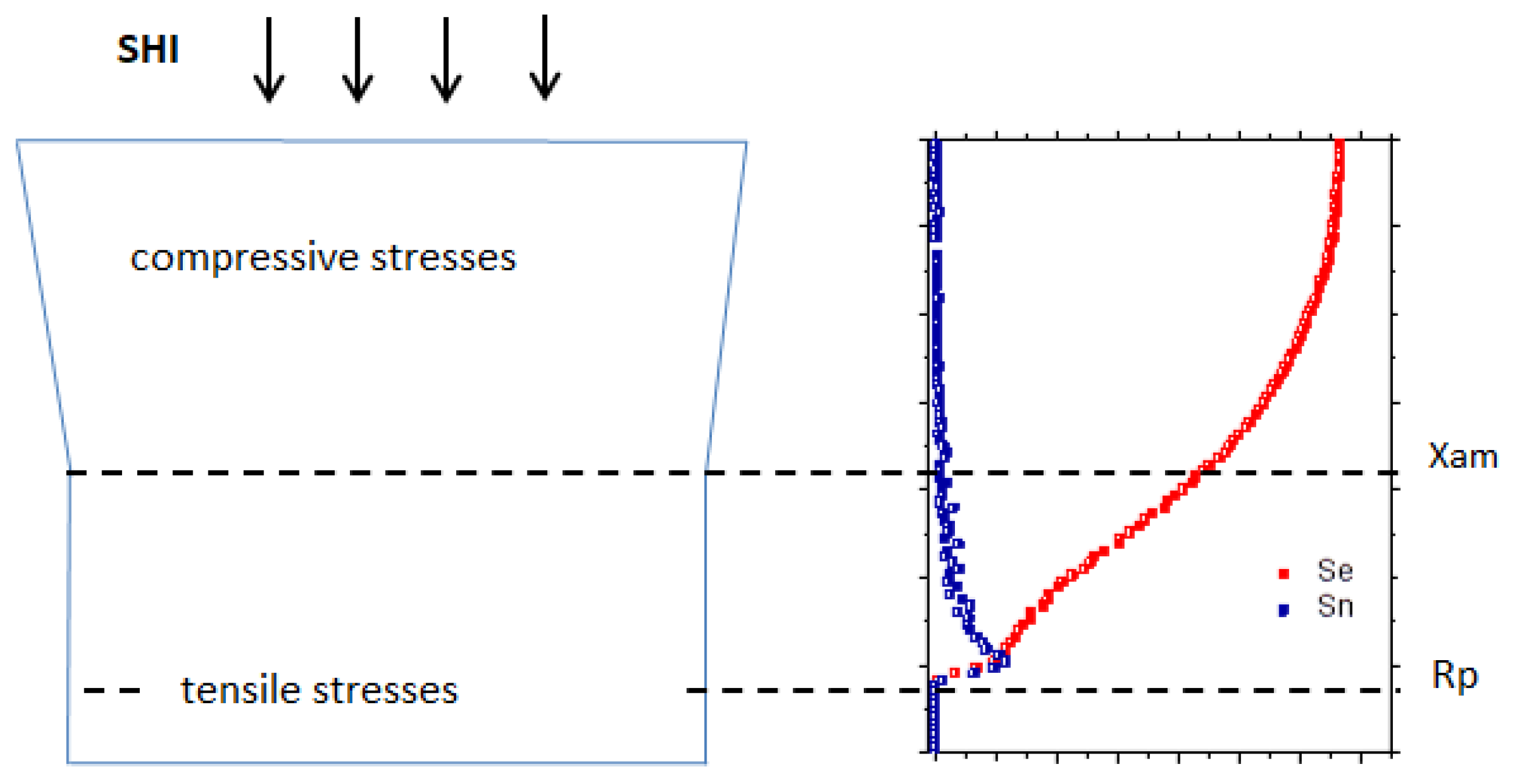
3.1. Amorphization

Before discussing the experimental results, let us briefly consider the literature data on the Raman spectra in silicon nitride. Currently, there are 12 peaks that are associated with β-Si3N4: five of them are Ag, two are E1g, and five are E2g symmetry. The authors of [23] observed 11 peaks in their work, 10 of which confirmed the previous experimental data and agree well with theoretical calculations [24]. They predict the unobservable Ag mode at 457 cm−1 and estimate its cross section to be many times smaller than that of the E2g mode at 444 cm−1, thus explaining why this peak remained unrecorded in this region. In their study, the authors of [25] also observed 11 peaks for β-Si3N4, including a peak at 144 cm−1. Sergo V. et al. [11] gives 10 peaks for β-Si3N4, excluding the lines at 144 and 457 cm−1. The Raman spectra of β-Si3N4 were also studied by Honda et al. [26], who recorded vibrational modes by analyzing polarized spectra that was performed with a change in the direction of incidence of the laser beam and the angle of reflected scattered light. The most intense Raman bands at 183, 204, and 227 cm−1 were attributed to the vibrational modes of the lattice, and the remaining bands in the region from 300 to 1200 cm−1 assigned to internal modes were attributed to the internal modes [25,27].
In this work, the Raman spectra of the initial silicon nitride sample has 10 peaks, as can be seen from Table 2, which also presents the literature data [11,23,24,25,26,28].
Figure 1 shows the dose dependence of the Raman spectra that was measured from the surface of Si3N4 samples that were irradiated with xenon and bismuth ions. As can be seen from the figure, with increasing ion fluence, a broadening of the lines of all of the crystalline vibrational modes is detected, as well as a reduction in their intensity to an undetectable level. This was registered at fluences of 4 × 1013 cm−2 for Xe ions and 1 × 1013 cm−2 for Bi ions. Such behavior was observed in many swift heavy ion (SHI) bombarded solids, particularly in oxides and was attributed to lattice disorder up to the transition to amorphous state, and the strain-induced distortion of the bonds that were associated with the corresponding radiation damage formation (for example, [29,30,31]).
As was found earlier, 167 MeV xenon ion irradiation results in the formation of discontinuous tracks in polycrystalline silicon nitride [14] and a complete loss of crystallinity can be ascribed to multiple overlapping of ion track regions. The process of amorphization starts from the sub-surface layer, where the ionization energy losses are maximal for the given irradiation conditions, with a gradual propagation in depth as the fluence of the bombarding ions increases. Such evolution of defect structure was revealed in single crystalline Al2O3 that was irradiated by Xe ions with energies from 70 to 160 MeV [32]. At 710 MeV bismuth ions induce continuous amorphous tracks and the amorphous fraction increases with irradiation fluence as is predicted by a direct impact model [33].
Since the Raman signal intensity is highly dependent on the surface roughness, the FWHM of dominant 204 cm−1 Raman line was chosen as a possible parameter for comparing the spectra across the irradiated layer as a function of ion fluence. As already mentioned, an increase in the ion fluence leads to broadening of all of the spectral lines and, consequently, leads to an increase in the FWHM values. It should be noted that FWHM is not used as a quantitative measure of general lattice disorder. Figure 2 shows the change in the FWHM of 204 cm−1 Raman line over the thickness of the Si3N4 layer that was irradiated with xenon and bismuth ions.
As can be seen from the figure, the FWHM values are maximal near the surface for both types of ions, which also confirms the relationship between the structural changes and the electronic stopping power. The increase of FWHM for xenon ions at depths above 9 μm is most likely associated with the increasing contribution of defects that are formed via elastic collisions. As known, their concentration has maximum in the end of ion range.
Considering the data that are presented in Figure 2, one can see that FWHM was not determined in the layers with a thickness ~8 μm for Xe ion fluences that were higher than 2 × 1013 cm−2 and ~21 μm for Bi ion fluence 1013 cm−2 due to the low level of Raman signal. Referring to the TEM data [14,16,17] it is seems reasonable to suggest that the irradiated samples were amorphized to corresponding depth (marked by red dashed lines in Figure 2). Depths of 8 and 21 μm correspond to 10.6 keV/nm and 20 keV/nm in energy loss profiles for Xe and Bi ions, respectively. It should be noted that these electronic stopping powers cannot be taken as the threshold values that are needed for amorphization of the material. It is reasonable to suggest that reason for such differences is the different track size and morphology. The production of continuous amorphous tracks by Bi ions, as mentioned above, leads to conclusion that the amorphization process obeys direct impact mechanisms and that the thickness of the amorphized layer is defined by the track radius and fluence, when single tracks start to overlap. Since the track size is Se dependent, there is a direct connection between the track radius and thickness of the amorphized layer, in which the complete loss of crystallinity starts from the surface where the track radius is maximal.
Amorphization by Xe ions requires multiple overlapping of track regions, that is, the passage of at least several ions through the same area. Therefore, the total energy deposition per unit length is summarized from the energy loss of single ions. This can explain why the Se value that designates the amorphization depth for Xe ions is less than that for Bi ions.
Another estimate of size of the amorphized layer was done using SEM imaging of the edge of silicon nitride specimens that were irradiated with Xe ions. An example of the images for the initial and irradiated samples to a fluence of 3.2 × 1013 cm−2 is shown in Figure 3. As can be seen, the thickness of the possibly amorphized layer is ~8 µm (ion projected range Rp = 13.4 µm), which practically coincides with the data that were deduced from the Raman spectra by measuring the depth profiles of FWHM of the 204 cm−1 line. At the same time, we note that both the Raman spectroscopy as well as SEM technique cannot be used for quantitative evaluation of amorphized layer thickness.

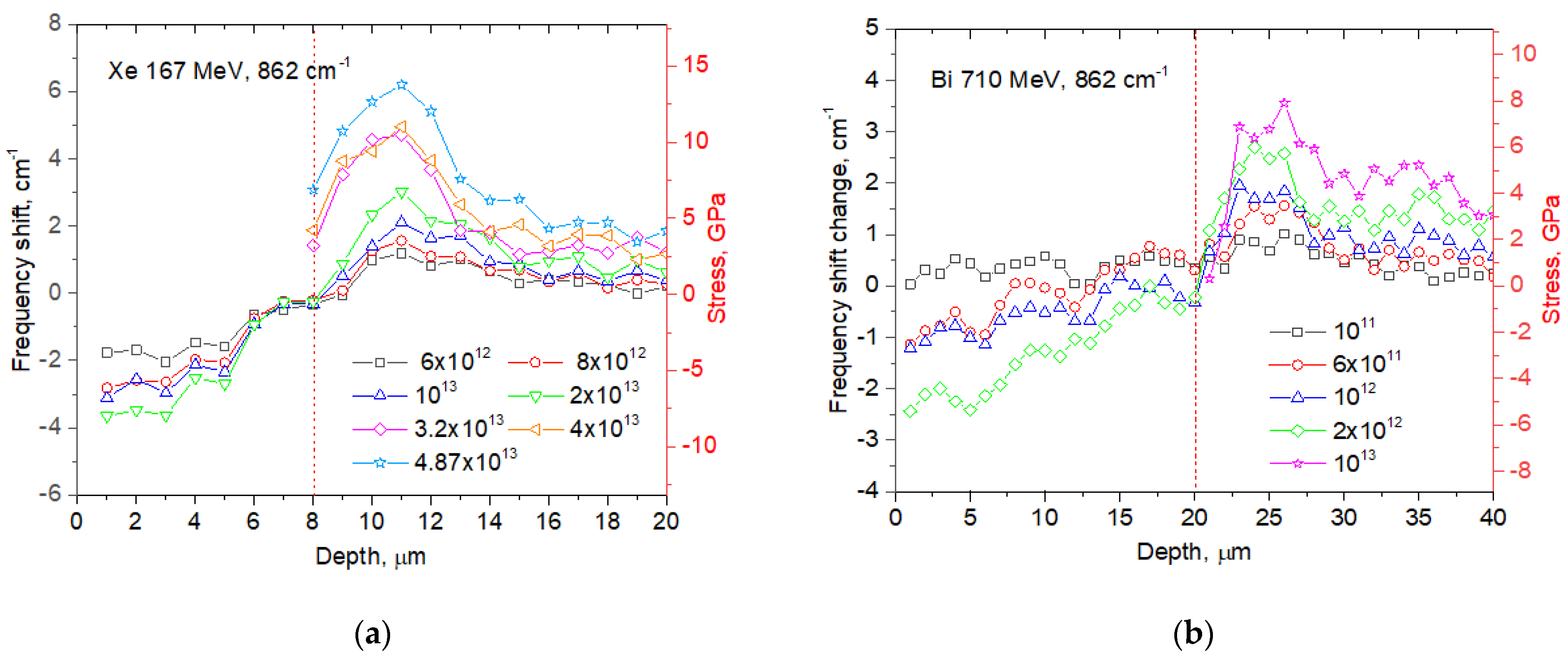
3.2. Mechanical Stress

The registration of shifts in the position of peaks in the Raman spectra at different depths of ion penetration make it possible to find the profiles of mechanical stresses that are caused by irradiation with high-energy xenon and bismuth ions. This is done using the known relationships between frequency shifts in the Raman spectra and the level of applied or residual mechanical stresses (for example, [1,34]). It should be noted that the parameters of stress fields in silicon nitride that have been irradiated with heavy ions with fission fragment energies have not been studied previously.
Figure 4 shows the changes in the spectral position of the 862 cm−1 line over the depth of the irradiated layer. This line was chosen to estimate the stress level, since it is characterized by the highest piezospectroscopic coefficient, 2.22 GPa/cm−1 [34].
Another advantage of using this line is that it is separated from the other lines (see Figure 1), which greatly simplifies the procedure for accurately determining the position of the peak. Honda et al. [26] in their study showed that the E1g mode, corresponding to the Raman band at about 866 cm−1, is relatively sensitive to stress, which justifies its use in the stress level estimates. In [11], the band shifts of 183, 205, 226, 862, 925, and 937 cm−1 were analyzed. It was found that the corresponding PS coefficients for β-Si3N4 were positive for the triplet mode at approximately 200 cm−1, which additionally confirms the hypothesis that these bands are due to external vibrational modes [25,27]. Unfortunately, despite the high signal–noise ratio, these three peaks show a rather weak dependence on the stresses [11,34], which reduces the measurement accuracy.
The data that are presented in Figure 4, demonstrate the mechanical stress profiles in the irradiated silicon nitride samples. The scheme, illustrating the structure of the layer that is affected by SHI is given in Figure 5 together with the energy loss profiles. Due to the that fact that the density of the amorphous phase is less than the density of the crystalline phase, the formation of amorphous tracks results in volume expansion (swelling) that induces the hydrostatic compressive stresses that were detected. This was evidenced by the shift to lower frequencies, starting from the surface to a depth that determines the size of the layer that was amorphized at high fluences. At higher depths, the sign of the stresses changes to the opposite (tensile) to compensate for compressive stresses. The stress level gradually decreases to the initial level, at a depth that significantly exceeds the ion projected range Rp. Since the Raman tensorial formalism of stress analysis is irrelevant in polycrystalline or amorphous materials, no information about the strain anisotropy can be deduced and we detect strain that was averaged for x-, y-, and z-directions.
The maximum positive shifts of the 862 cm−1 line were approximately 6 cm−1 for xenon ions and 4 cm−1 for bismuth ions, that, taking into account the above PS coefficient, corresponds to 13.2 GPa and 8.8 GPa, respectively. This significantly exceeds the maximum tensile strength values that are known from the literature, 2.5 GPa. We have noted that the maximal tensile stresses are registered at depth that is less than maximum of the nuclear stopping power and that role of the defects that are formed in elastic collisions in this effect remains unclear.
The accumulation of compressive mechanical stresses that are due to the formation of latent tracks was observed in a number of ceramics that were irradiated with swift heavy ions, in particular in Al2O3 [10] and ZrO2:Y2O3 [35,36,37]. Therefore, the compressive stress that was detected in silicon nitride can be considered as a universal phenomenon that is typical for SHI amorphizable solids. In our case, it can be argued that the compressive mechanical stresses are accumulated in the zone of formation of latent tracks, regardless of their morphology, whether that be amorphous continuous (Bi), or amorphous discontinuous (Xe). At the same time, the amplitude of the tensile stresses that were beyond the boundary of this region can exceed the amplitude of the compressive stresses in the subsurface region (Figure 4), which is a peculiarity that is found so far only for silicon nitride. For example, the measurements of the stress profiles in Al2O3 single crystals that were irradiated with Xe and Bi ions with the same energies as in this work also showed a correlation between the electronic stopping power and the level of stresses in the region of latent track formation [10]. However, the amplitude of the compressive stresses at a higher depth was within the accuracy of the measurements, in contrast to Si3N4. The reason for the observed differences could be both the different morphology of the tracks (ion track regions in Al2O3 remain crystalline) and the properties of the materials themselves, which requires further research.

4. Conclusions

The depth profiles of the residual mechanical stresses that were induced by high-energy xenon and bismuth ions in polycrystalline silicon nitride were measured using Raman spectroscopy. The stresses were determined from the shift of the 862 cm−1 line in the Raman spectra using the known piezospectroscopic coefficient. It was found that both the compressive and tensile mechanical stresses are accumulated in the irradiated layer. It is assumed that the compressive stresses are registered in the region where the latent tracks are produced. Beyond this zone, the tensile stresses are detected up to depths that exceed the projective range of xenon and bismuth ions.
The dose dependence of the FWHM of the main line at 204 cm−1 was used for rough estimates of the size of the region that was amorphized due to multiple ion tracks overlapping. The data that were obtained are consistent with those that were deduced from scanning electron microscopy.

Author Contributions

Conceptualization, A.Z., A.I., A.D., V.S.; methodology, A.M., E.K., A.Z.; validation, A.A., M.Z., A.D.; formal analysis, A.Z., A.M., V.S., A.D., investigation, A.Z., A.I., A.M., E.K.; resources: A.A., M.Z., V.S., A.D.; data curation: A.Z., A.M.; writing—original draft preparation: A.Z., A.M.; writing—review and editing, A.Z., V.S.; visualization: A.M., V.S., E.K.; supervision, A.D., A.A., V.S., M.Z.; project administration, A.D., A.A.; funding acquisition, A.D., A.A. All authors have read and agreed to the published version of the manuscript.

Funding

The work was funded by Ministry of Education and Science of the Republic of Kazakhstan, grant No AP 08856368.

Acknowledgments

The authors thank the staff of the IC-100 and U-400 FLNR JINR cyclotrons.

Conflicts of Interest

The authors declare no conflict of interest.

References

  1. Murari, N.; Sergo, V.; Pezzotti, G.; Katagiri, G.; Meriani, S.; Nishida, T. Raman Piezo-Spectroscopic Behavior of Aluminum Nitride. Appl. Spectrosc. 1997, 51, 1761–1765. [Google Scholar] [CrossRef]
  2. Pezzotti, G. Measurements of microscopic stresses in si-based polycrystalline ceramics. Key Eng. Mater. 2005, 287, 438–448. [Google Scholar] [CrossRef]
  3. Ma, Q.; Clarke, D.R. Stress Measurement in Single-Crystal and Polycrystalline Ceramics Using Their Optical Fluorescence. J. Am. Ceram. Soc. 1993, 76, 1433–1440. [Google Scholar] [CrossRef]
  4. Molis, S.E.; Clarke, D.R. Measurement of Stresses Using Fluorescence in an Optical Microprobe: Stresses around Indentations in a Chromium-Doped Sapphire. J. Am. Ceram. Soc. 1990, 73, 3189–3194. [Google Scholar] [CrossRef]
  5. Forman, R.A.; Piermarini, G.J.; Barnett, J.D.; Block, S. Pressure Measurement Made by the Utilization of Ruby Sharp-Line Luminescence. Science 1972, 176, 284–285. [Google Scholar] [CrossRef]
  6. Sergo, V.; Clarke, D.R.; Pompe, W. Deformation Bands in Ceria-Stabilized Tetragonal Zirconia/Alumina: I, Measurement of Internal Stresses. J. Am. Ceram. Soc. 1995, 78, 633–640. [Google Scholar] [CrossRef]
  7. Skuratov, V.A.; Bujnarowski, G.; Kovalev, Y.S.; Havanscak, K. Piezospectroscopic study of mechanical stress in Al2O3:Cr under swift heavy ion irradiation. Vacuum 2009, 83, 65–68. [Google Scholar] [CrossRef]
  8. Bujnarowski, G.; Skuratov, V.A.; Havancsak, K.; Kovalev, Y.S. Accumulation of mechanical stress in Al2O3: Cr under swift heavy ion irradiation. Radiat. Eff. Defects Solids 2009, 164, 409–416. [Google Scholar] [CrossRef]
  9. Skuratov, V.A.; Bujnarowski, G.; Kovalev, Y.S.; O’Connell, J.; Havanscak, K. In situ and postradiation analysis of mechanical stress in Al2O3:Cr induced by swift heavy-ion irradiation. Nucl. Instrum. Methods Phys. Res. B 2010, 268, 3023–3026. [Google Scholar] [CrossRef]
  10. Skuratov, V.A.; Kirilkin, N.S.; Kovalev, Y.S.; Strukova, T.S.; Havanscak, K. Depth-resolved photo- and ionoluminescence of LiF and Al2O3. Nucl. Instrum. Methods Phys. Res. B 2012, 286, 61–66. [Google Scholar] [CrossRef]
  11. Sergo, V.; Pezzotti, G.; Katagiri, G.; Muraki, N.; Nishida, T. Stress Dependence of the Raman Spectrum of β-Silicon Nitride. J. Am. Ceram. Soc. 1996, 79, 781–784. [Google Scholar] [CrossRef]
  12. Zinkle, S.J.; Skuratov, V.A.; Hoelzer, D.T. On the conflicting roles of ionizing radiation in ceramics. Nucl. Instrum. Methods Phys. Res. Sect. B Beam Interact. Mater. At. 2002, 191, 758–766. [Google Scholar] [CrossRef]
  13. Janse van Vuuren, A.; Ibrayeva, A.; Skuratov, V.; Zdorovets, M. Analysis of the microstructural evolution of silicon nitride irradiated with swift Xe ions. Ceram. Int. 2020, 46, 7155–7160. [Google Scholar] [CrossRef]
  14. Janse van Vuuren, A.; Skuratov, V.; Ibrayeva, A.; Zdorovets, M. Microstructural Effects of Al Doping on Si3N4 Irradiated with Swift Heavy Ions. Acta Phys. Pol. A 2019, 136, 241–244. [Google Scholar] [CrossRef]
  15. Kitayama, T.; Morita, Y.; Nakajima, K.; Narumi, K.; Saitoh, Y.; Matsuda, M.; Sataka, M.; Tsujimoto, M.; Isoda, S.; Toulemonde, M.; et al. Formation of ion tracks in amorphous silicon nitride films with MeV C60 ions. Nucl. Instrum. Methods Phys. Res. Sect. B Beam Interact. Mater. At. 2015, 356, 22–27. [Google Scholar] [CrossRef]
  16. Janse Van Vuuren, A.; Ibrayeva, A.; Rymzhanov, R.A.; Zhalmagambetova, A.; O’Connell, J.H.; Skuratov, V.A.; Uglov, V.V.; Zlotski, S.V.; Volkov, A.E.; Zdorovets, M. Latent tracks of swift Bi ions in Si3N4. Mater. Res. Express 2020, 7, 025512. [Google Scholar] [CrossRef]
  17. Janse van Vuuren, A.; Ibrayeva, A.D.; O’Connell, J.H.; Skuratov, V.A.; Mutali, A.; Zdorovets, M.V. Latent ion tracks in amorphous and radiation amorphized silicon nitride. Nucl. Instrum. Methods Phys. Res. Sect. B 2020, 473, 16–23. [Google Scholar] [CrossRef]
  18. Canut, B.; Ayari, A.; Kaja, K.; Deman, A.L.; Lemiti, M.; Fave, A.; Souifi, A.; Ramos, S. Ion-induced tracks in amorphous Si3N4 films. Nucl. Instrum. Methods Phys. Res. Sect. B Beam Interact. Mater. At. 2008, 266, 2819–2823. [Google Scholar] [CrossRef]
  19. Morita, Y.; Nakajima, K.; Suzuki, M.; Narumi, K.; Saitoh, Y.; Ishikawa, N.; Hojou, K.; Tsujimoto, M.; Isoda, S.; Kimura, K. Surface effect on ion track formation in amorphous Si3N4 films. Nucl. Instrum. Methods Phys. Res. Sect. B Beam Interact. Mater. At. 2013, 315, 142–145. [Google Scholar] [CrossRef]
  20. Ibrayeva, A.; Janse van Vuuren, A.; Skuratov, V.A.; Zdorovets, M.V.; O’Connell, J.H. Applicability of the i-TS Model to Evaluation of Latent Track Parameters in Silicon Nitride. In Proceedings of the 20th International Conference «Radiation Effects in Insulators», Nur-Sultan (Astana), Kazakhstan, 19–23 August 2019; p. 157. [Google Scholar]
  21. Janse van Vuuren, A.; Ibrayeva, A.; Skuratov, V.A.; Zdorovets, M.V. iTS Model-Based Analysis of Track Formation in Crystalline and Amorphous Silicon Nitride. In Proceedings of the 13th International Conference of the Interaction of Radiation with Solids, Minsk, Belarus, 30 September–3 October 2019; pp. 97–99. [Google Scholar]
  22. Ziegler, J.F.; Ziegler, M.D.; Biersack, J.P. SRIM—The stopping and range of ions in matter. Nucl. Instrum. Methods Phys. Res. Sect. B Beam Interact. Mater. At. 2010, 268, 1818–1823. [Google Scholar] [CrossRef] [Green Version]
  23. Vogelgesang, R.; Grimsditch, M.; Wallace, J.S. Polarized ultraviolet Raman spectroscopy of β-Si3N4. J. Appl. Phys. 2002, 92, 3103–3106. [Google Scholar] [CrossRef]
  24. Dong, J.; Sankey, O.F. Assignment of the Raman active vibration modes of β-Si3N4 using micro-Raman scattering. J. Appl. Phys. 2000, 87, 958–959. [Google Scholar] [CrossRef]
  25. Wada, N.; Solin, S.A.; Wong, J.; Prochazk, S. Raman and IR absorption spectroscopic studies on α, β, and amorphous Si3N4. J. Non-Cryst. Solids 1981, 43, 7–15. [Google Scholar] [CrossRef]
  26. Honda, K.; Yokoyama, S.; Tanaka, S. Assignment of the Raman active vibration modes of β-Si3N4 using micro-Raman scattering. J. Appl. Phys. 1999, 85, 7380. [Google Scholar] [CrossRef]
  27. Takase, E.; Tani, E. Low-frequency Raman spectra of sintered Si3N4 under gas pressure. J. Mater. Sci. Lett. 1987, 6, 607. [Google Scholar] [CrossRef]
  28. Cai, Y.; Zeng, Q.; Zhang, L.; Cheng, L.; Xu, Y. First-principles study of vibrational and dielectric properties of β-Si3N4. J. Phys. Rev. B 2006, 74, 174301. [Google Scholar] [CrossRef] [Green Version]
  29. Park, S.; Lang, M.; Tracy, C.L.; Zhang, J.; Zhang, F.; Trautmann, C.; Patrick, K.; Rodriguez, M.D.; Ewing, R.C. Swift heavy ion irradiation-induced amorphization of La2Ti2O7. Nucl. Instrum. Methods Phys. Res. Sect. B Beam Interact. Mater. At. 2014, 326, 145–149. [Google Scholar] [CrossRef]
  30. Tracy, C.L.; Pray, J.M.; Lang, M.; Popov, D.L.; Park, C.; Trautmann, C.; Ewing, R.C. Defect accumulation in ThO2 irradiated with swift heavy ions. Nucl. Instrum. Methods Phys. Res. Sect. B Beam Interact. Mater. At. 2014, 326, 169–173. [Google Scholar] [CrossRef]
  31. Park, S.; Tracy, C.L.; Zhang, F.; Park, C.; Trautmann, C.; Tkachev, S.N.; Lang, M.; Mao, M.L.; Ewing, R.C. Radiation-induced disorder in compressed lanthanide zirconates. Phys. Chem. Chem. Phys. 2018, 20, 6187–6197. [Google Scholar] [CrossRef]
  32. Okubo, N.; Ishikawa, N.; Sataka, M.; Jitsukawa, S. Surface amorphization in Al2O3 induced by swift heavy ion irradiation. Nucl. Instrum. Methods Phys. Res. B 2013, 314, 208–210. [Google Scholar] [CrossRef]
  33. Weber, W. Models and mechanisms of irradiation-induced amorphization in ceramics. Nucl. Instrum. Methods Phys. Res. Sect. B Beam Interact. Mater. At. 2000, 166–167, 98–106. [Google Scholar] [CrossRef]
  34. Muraki, N.; Katagiri, G.; Sergo, V.; Pezzotti, G.; Nishida, T. Mapping of residual stresses around an indentation in β-Si3N4 using Raman spectroscopy. J. Mater. Sci. 1997, 32, 5419–5423. [Google Scholar] [CrossRef]
  35. Sattonnay, G.; Moll, S.; Herbst-Ghysel, M.; Legros, C.; Costantini, J.M.; Thomé, L. Mechanical stresses induced in ceramic oxides by ion irradiation. Nucl. Instrum. Methods Phys. Res. Sect. B 2008, 266, 3052–3056. [Google Scholar] [CrossRef]
  36. Sattonnay, G.; Lahrichi, M.; Herbst-Ghysel, M.; Garrido, F.; Thomé, L. Stress field induced by swift heavy ion irradiation in cubic yttria stabilized zirconia. J. Appl. Phys. 2007, 101, 103516. [Google Scholar] [CrossRef]
  37. Sattonnay, G.; Lahrichi, M.; Benyagoub, A.; Costantini, J.M.; Garrido, F.; Thome, L.; Trautmann, C. Structural modifications induced by swift heavy ions in cubic stabilized zirconia: An X-ray diffraction investigation. Nucl. Instrum. Methods Phys. Res. B 2007, 257, 476–479. [Google Scholar] [CrossRef]
Figure 1. The dose dependence of Raman spectra of Si3N4 irradiated with (a) Xe (167 MeV) and (b) Bi (710 MeV) ions. The dashed lines indicate positions of 862 cm−1 and 1045 cm−1 lines.
Crystals 11 01313 g001
Figure 2. Nuclear (Sn) and ionization (Se) energy loss profiles and variation of the FWHM of 204 cm−1 line depth profiles with Xe and Bi ion fluence.
Crystals 11 01313 g002
Figure 3. SEM images of the edge of (a) initial and (b) 167 MeV Xe ion irradiated (3.2 × 1013 cm−2) silicon nitride samples. The direction of the ion beam incidence is indicated by an arrow. The border of the amorphized layer is marked with a dashed line.
Crystals 11 01313 g003
Figure 4. Variation of the spectral position of the 862 cm−1 line over the depth of the irradiated layer for different (a) Xe and (b) Bi ion fluences.
Crystals 11 01313 g004
Figure 5. Schematic drawing of SHI irradiated target and energy loss profiles.
Crystals 11 01313 g005
Table 1. The ion irradiation parameters.
IonEnergy,
MeV
Se,
keV/nm
Rp,
μm
Fluence,
cm−2
132Xe16720.813.46 × 1012, 8 × 10¹², 1 × 10¹³,
2 × 10¹³, 3.2 × 10¹³, 4 × 10¹³,
4.87 × 10¹³
209Bi71033.629.81 × 1011, 6 × 10¹¹, 1 × 10¹², 2 × 10¹², 1 × 10¹³
Table 2. Theoretical and experimental parameters of the Raman spectra in β-Si3N4.
TheoryExperiment
[24][25][28][11][26][23]This work
144 (145)Ag Ag
183E2g186181183185E2g182E2g183.33E2g
201Ag210200206208Ag204Ag203.61Ag
228E1g229225227230E1g225E1g226.71E1g
444E2g451444449452E2g447E2g449.38E2g
457Ag 456 Ag457Ag/E2g(?)
603E2g619610617620E2g613E2g614.24E2g
715Ag732725730733Ag727Ag729.82Ag
836E1g865859863866E1g856E1g862.70E1g
897E2g928921927730E2g921E2g927.22E2g
908Ag939930937940Ag932Ag938.78Ag
1012E2g1047102110451048E2g1039E2g1045.47E2g
Publisher’s Note: MDPI stays neutral with regard to jurisdictional claims in published maps and institutional affiliations.

