
Gated Silicon Drift Detector Fabricated from a Low-Cost Silicon Wafer

Abstract
: Inexpensive high-resolution silicon (Si) X-ray detectors are required for on-site surveys of traces of hazardous elements in food and soil by measuring the energies and counts of X-ray fluorescence photons radially emitted from these elements. Gated silicon drift detectors (GSDDs) are much cheaper to fabricate than commercial silicon drift detectors (SDDs). However, previous GSDDs were fabricated from 10-kΩ·cm Si wafers, which are more expensive than 2-kΩ·cm Si wafers used in commercial SDDs. To fabricate cheaper portable X-ray fluorescence instruments, we investigate GSDDs formed from 2-kΩ·cm Si wafers. The thicknesses of commercial SDDs are up to 0.5 mm, which can detect photons with energies up to 27 keV, whereas we describe GSDDs that can detect photons with energies of up to 35 keV. We simulate the electric potential distributions in GSDDs with Si thicknesses of 0.5 and 1 mm at a single high reverse bias. GSDDs with one gate pattern using any resistivity Si wafer can work well for changing the reverse bias that is inversely proportional to the resistivity of the Si wafer.1. Introduction
Various types of X-ray detectors, such as silicon (Si) pin detectors and silicon drift detectors (SDDs) [1–29], are used to measure the energy and photon count of X-ray fluorescence photons. Si X-ray detectors with a thick Si substrate, a large active area, and small capacitance are desirable [29–32].
A pin structure is used to collect charge carriers, the number of which are proportional to the energy of an X-ray photon. In X-ray fluorescence spectroscopy, the capacitance of a pin detector increases with the active area of the detector because the anode (n-type layer) and the cathode (p-type layer) have equal areas. The increase in the capacitance degrades its performance. However, SDDs have a much smaller capacitance than pin detectors [1]. This is because the anode, which is on one surface of the n− Si substrate (n− or i-layer), is much smaller than the pin detector, whereas the entrance window layer, which is the cathode on the opposite surface, is kept large [1]. The anode is surrounded by multiple p-type rings (p-rings), to which a different bias voltage is applied. The resulting electric field makes the electrons flow smoothly toward the anode. To form a sufficiently strong electric field toward the anode in the SDD, the p-rings are electrically coupled with expensive built-in metal-oxide-semiconductor field-effect transistors (MOSFETs) or implanted resistors.
To fabricate low-cost X-ray detectors, we have designed several simple-structure SDDs without MOSFETs or implanted resistors [33–43], one of which is a gated silicon drift detector (GSDD) [37,38,40–43]. In GSDDs fabricated by using a 0.625-mm-thick n− Si substrate with a resistivity (ρSi) of 10 kΩ·cm, an energy resolution of 145 eV at 5.9 keV was obtained from a 55Fe source at −38 °C [41]. The effective active area of the detector was approximately 18 mm2 by irradiating X-ray photons through a 0.1-mm-diameter pinhole [40].
The 10-kΩ·cm Si wafers are more expensive than the 2-kΩ·cm Si wafers used in commercial SDDs. In the present study, to fabricate much cheaper X-ray detectors, we used a device simulation to design adequate gate patterns for GSDDs formed from 2-kΩ·cm Si wafers.
2. Structure and Advantages of Gated Silicon Drift Detectors
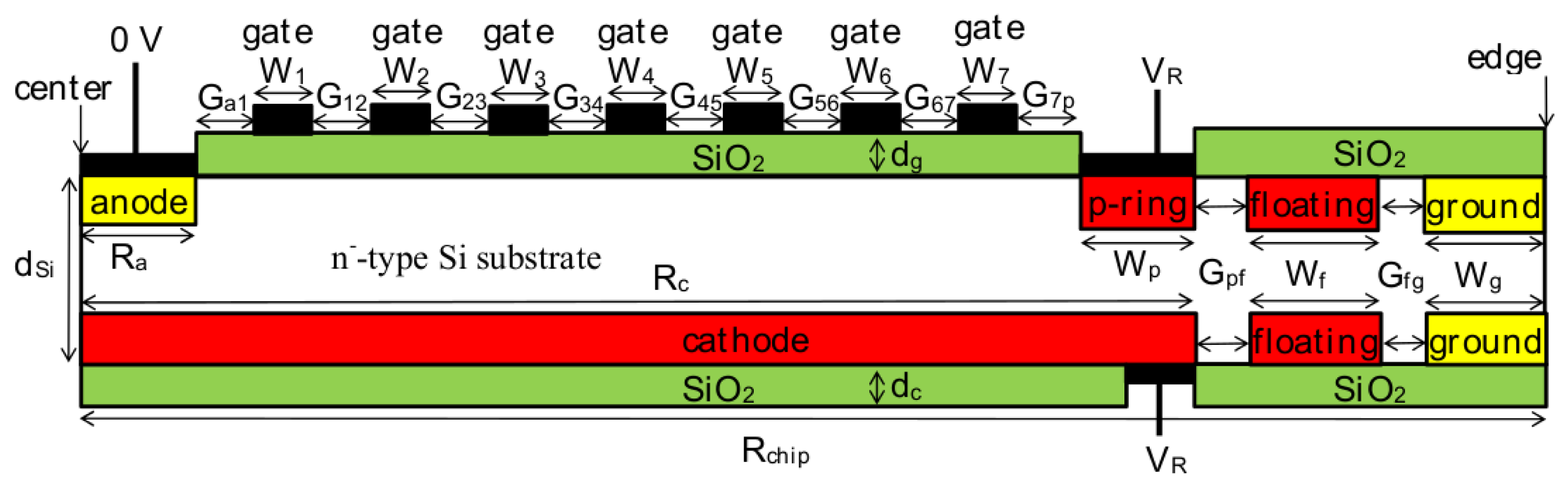
GSDDs have a cathode and only one p-ring, and to which the same reverse bias can be applied. Figure 1 shows half of a schematic cross section of a cylindrical GSDD with seven ring-shaped gates and one p-ring that does not contain MOSFETs or implanted resistors [37,38,40–43].
In SDDs and GSDDs, n-type layers (anode and ground rings) and p-type layers (cathode, p-ring, and floating rings) are fabricated by the same processes. In SDDs, multiple inner p-rings located between the anode and the p-ring are formed. Compared with GSDDs, the extra fabrication processes in SDDs are for creating the built-in MOSFETs or implanted resistors to couple the p-rings together electrically, which lowers the yield rate of detectors. The passivating oxide layers (SiO2) are formed, and the anode, p-ring, ground rings, and cathode are metallized. During metallization, the innermost p-ring is also metallized in SDDs, whereas gates are formed in GSDDs.
In GSDDs, no extra fabrication processes are required to form the gates because the metal gates are formed on the SiO2 during metallization of the anode and the p-ring. As a result, the fabrication of GSDDs is much simpler than that of commercial SDDs. Moreover, the same high reverse bias can be applied to the cathode, the p-ring, and all the gates, which means that GSDDs require only one high-voltage source. Therefore, GSDDs greatly reduce the cost of the X-ray detection system.
3. Device Simulation Processes
The device simulations were carried out by using the ATLAS Device Simulator (Silvaco International). All the simulations were performed by solving Poisson's equation and the carrier continuity equations. This provides a complete description of the system in terms of electrical quantities, such as electric potential and electric field distributions, carrier densities, and current densities.
The thicknesses of the n− Si substrate (dSi) were 0.5 and 1 mm, and the values of ρSi were 2 and 10 k Ω·cm. The radius of the anode (Ra) at the center of the cylindrical GSDD was fixed as 0.055 mm, which kept the capacitance of all GSDDs small. The widths of the p-ring (Wp), p-type floating rings (Wf), and n-type ground rings (Wg) were 0.545, 0.03 and 0.39 mm, respectively. The gap between the p-ring and the floating ring (Gpf) and the gap between the floating and ground rings (Gfg) were all 0.04 mm. The thickness of SiO2 on the cathode (dc) was 0.75 μm. The thickness of SiO2 on the other side (dg) was changed to constrain the electric field in the SiO2 between the gates and the Si substrate at ≤ 2.5 MV/cm, which is less than the SiO2 breakdown electric field of 10 MV/cm [44]. The sheet density of positive fixed charges in SiO2 near the SiO2/Si interface (QF) was fixed as 3 × 1010 cm−2, which has been reported for the present fabrication process [45]. The acceptor densities of the cathode, p-ring, and floating rings were 1 × 1018 cm−3, and the donor densities of the anode and ground rings were 1 × 1019 cm−3. The depths of the cathode, p-ring, anode, ground rings, and floating rings were all 1 μm.
Seven gates were considered in this study. Figure 1 shows that Ga1 was the gap between the anode and the innermost gate, and G12, G23, G34, G45, G56 and G67 were the gaps between the gates, from the innermost to outermost. G7p was the gap between the outermost gate and the p-ring. W1, W2, W3, W4, W5, W6 and W7 were the widths of the seven gates, from the innermost to outermost, respectively. The radii of the cathode (Rc = 3 mm) and the GSDD chip (Rchip = 3.5 mm) were fixed. As a result, the area inside the inner edge of the p-ring (Sarea) was 18.9 mm2, which is nearly equal to that of commercial small-area SDDs. The same reverse bias voltage(VR) was applied to the cathode, the p-ring, and all the gates.
4. Simulation Results and Discussion
4.1. 0.5-mm-Thick GSDD Formed from a 10-kΩ·cm Si Wafer
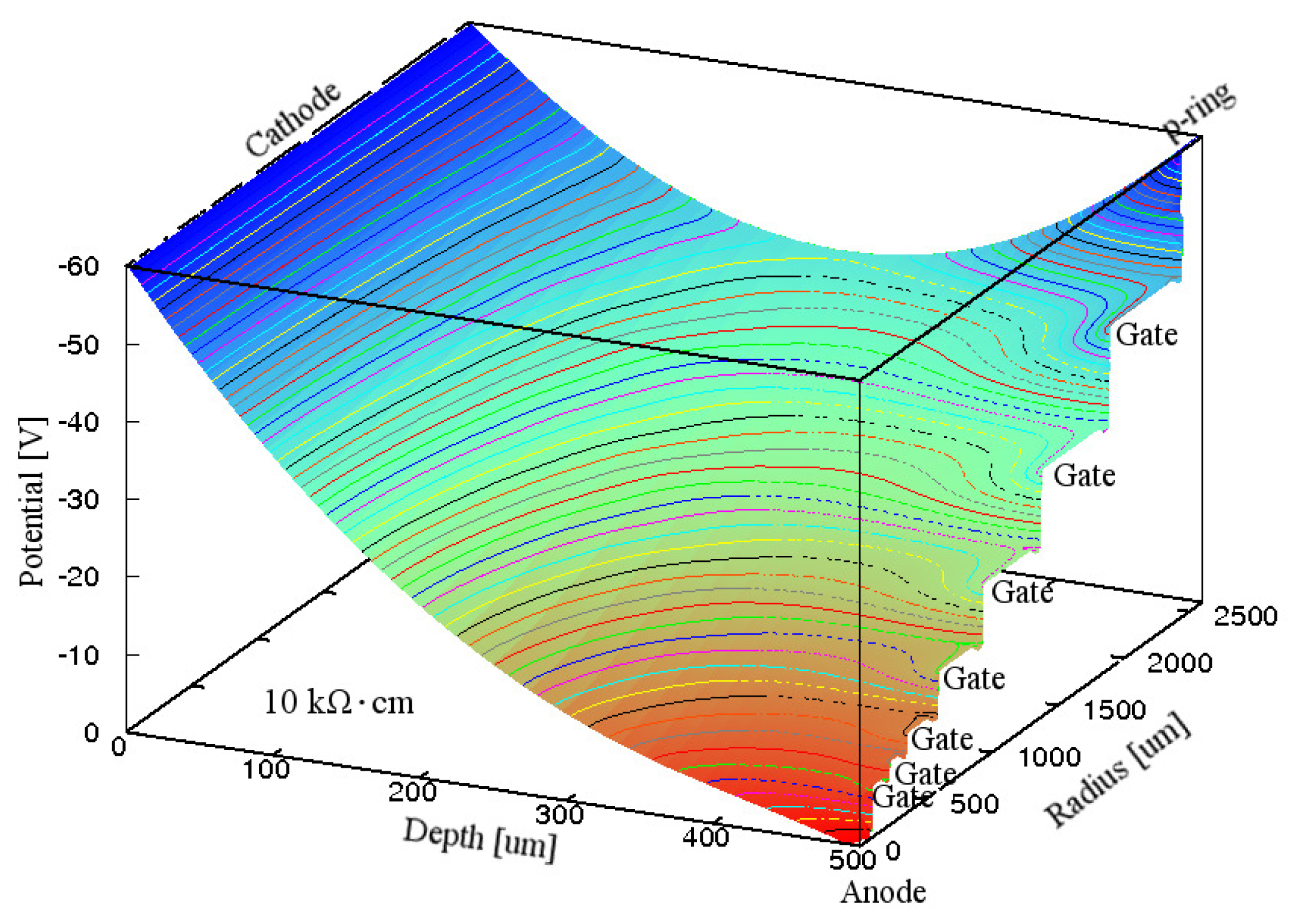
The dSi and ρSi of the n− Si substrate were 0.5 mm and 10 kΩ·cm, respectively, and dg was 0.75 μm. In Gate A, the values of W1, W2, W3, W4, W5, W6, and W7 were 0.1, 0.1, 0.19, 0.29, 0.39, 0.47 and 0.51 mm, respectively. Ga1 was 0.04 mm and G12 and G23 were both 0.03 mm. G34, G45, G56, G67 and G7p were all 0.05 mm.
Figure 2 shows the simulated electric potential distribution in the Si substrate inside the p-ring of the GSDD at VR of −60 V for Gate A. The voltage midway between the p-ring and the cathode was −37 V, and the electric field along the electric potential valley was strong enough to make all the electrons produced by an X-ray photon flow smoothly to the anode. Therefore, the electrons produced within the radius of the inner edge of the p-ring can be directed to the anode, indicating that the effective active area is approximately 18 mm2.
We fabricated GSDDs using the design of Gate A. In the GSDD, an energy resolution of 145 eV at 5.9 keV was obtained from a 55Fe source at −38 °C [41]. The effective active area of the detector was found to be approximately 18 mm2 by irradiating X-ray photons through a pinhole with diameter 0.1 mm [40], which is in good agreement with our simulation. These experimental results indicate that GSDDs with the design from which the simulated electric potential distribution similar to that in Figure 2 is obtained can work well.
4.2. 0.5-mm-Thick GSDD Formed from a 2-kΩ·cm Si Wafer
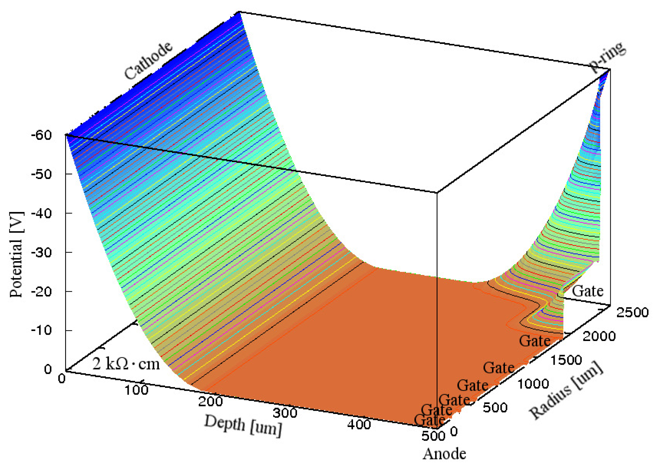
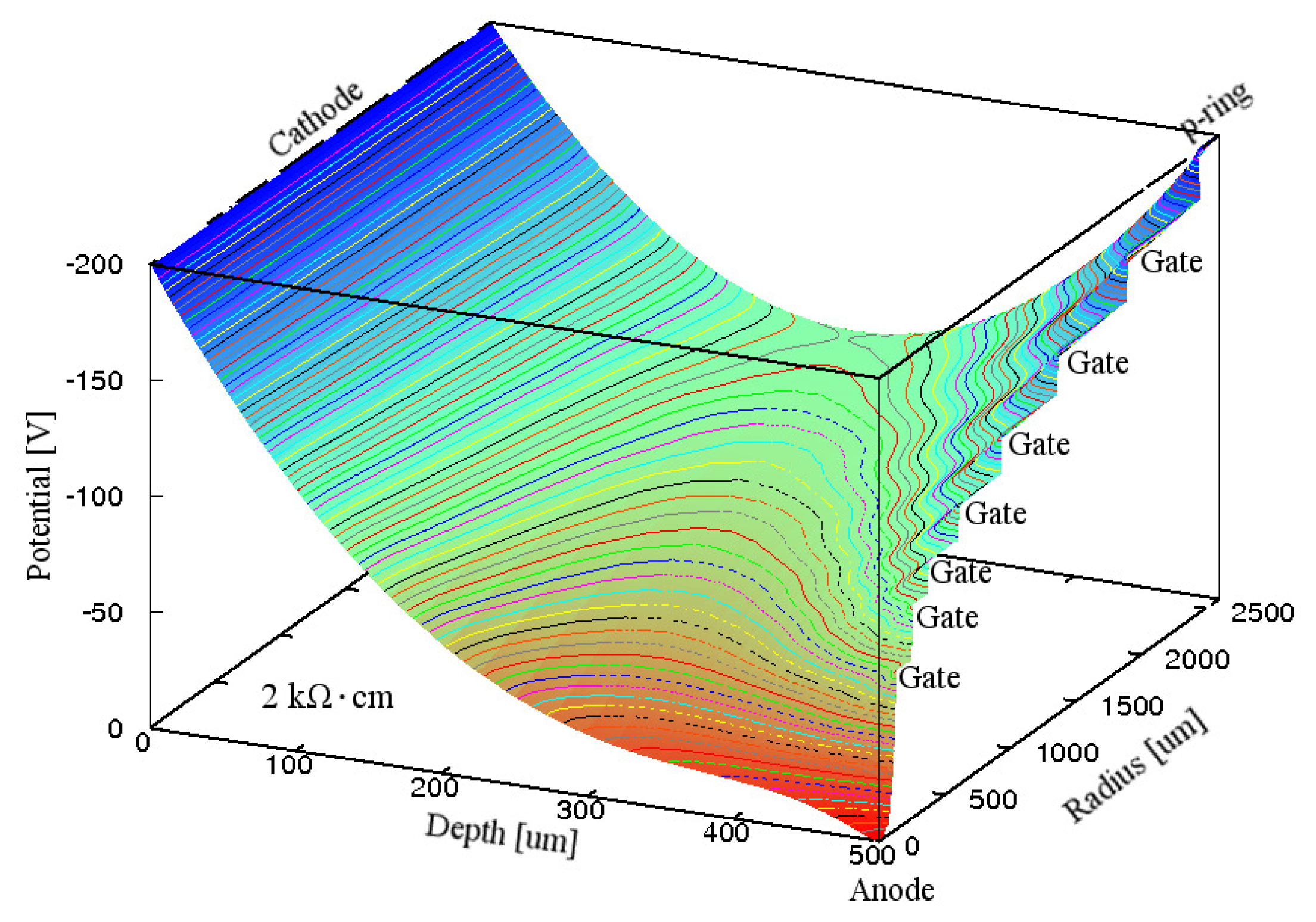
The value of ρSi was decreased from 10 kΩ·cm to 2 kΩ·cm. Figure 3 shows the simulated electric potential distribution in the Si substrate inside the p-ring of the GSDD with Gate A at VR of −60 V. Because the voltage drops at G67 and G7p were too large, the electric potential was almost zero between the anode and the outermost gate, and also over approximately 60% of the n− Si substrate, where the electrons produced by an X-ray photon are recombined with the holes produced by the X-ray photon.
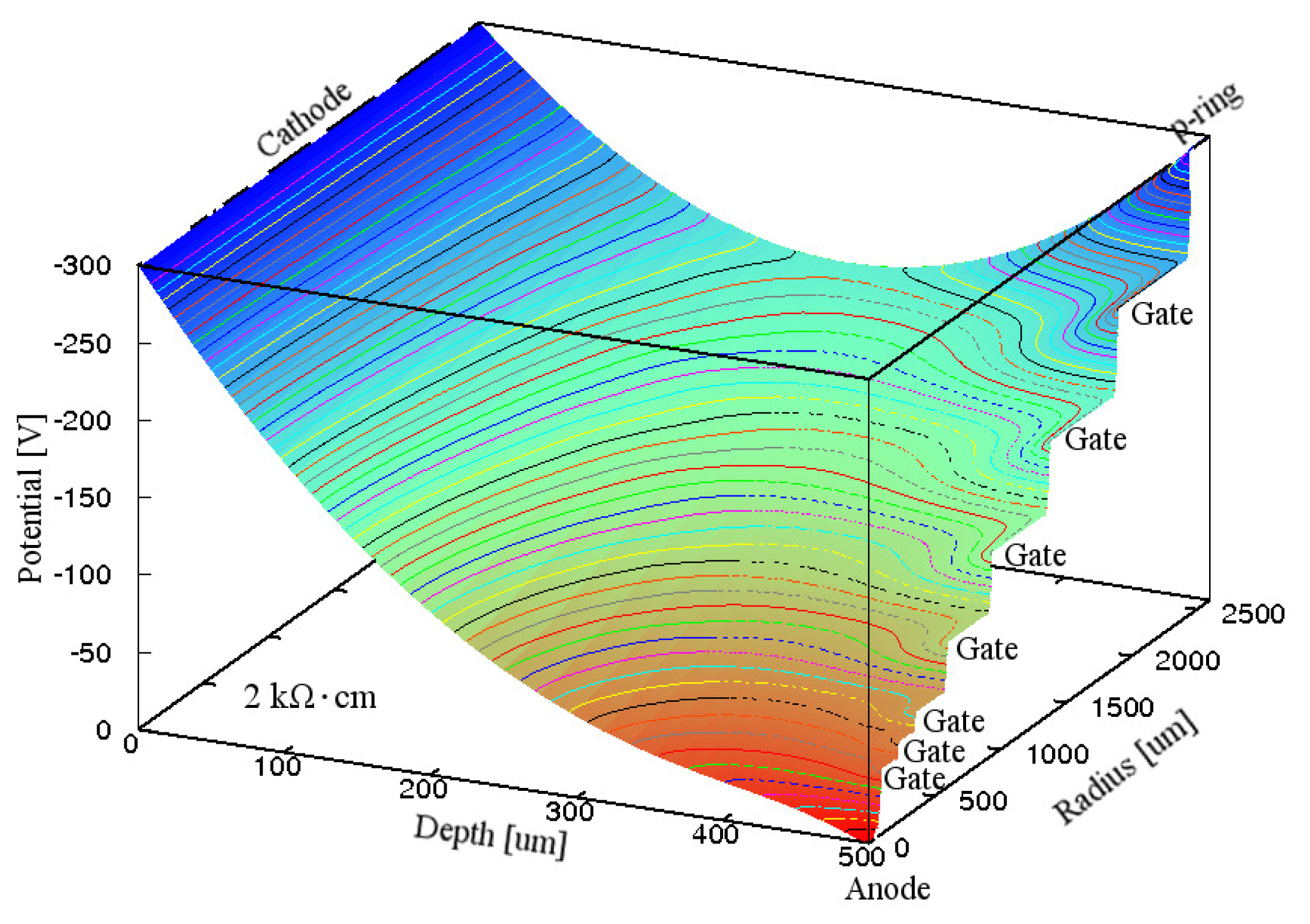
To deplete the whole n− Si substrate,VR was increased from −60 to −300 V, following the relation
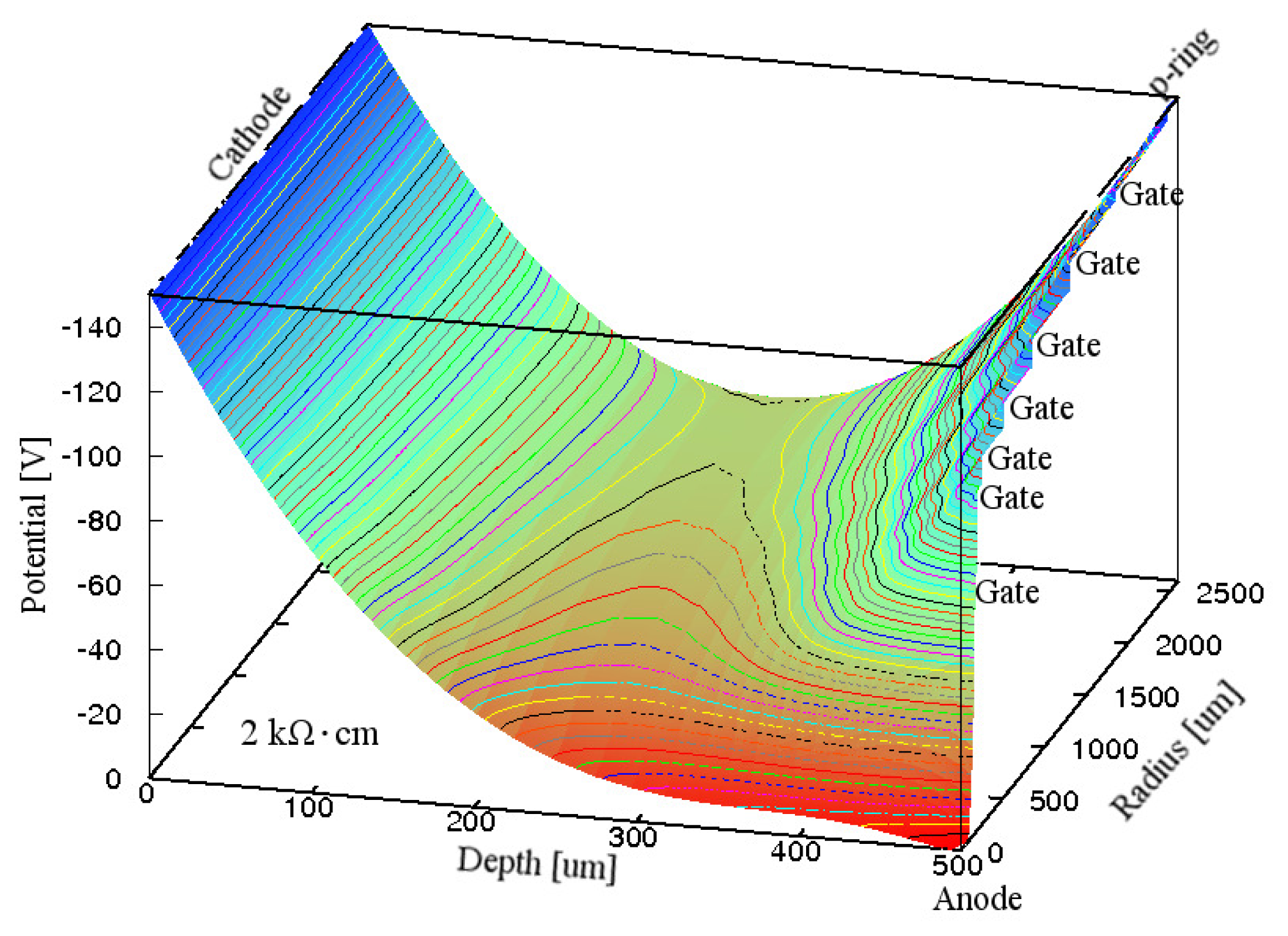
Figure 4 shows the simulated electric potential distribution in the Si substrate inside the p-ring of the GSDD with Gate A at VR of −300 V. It is clear from Figure 4 that the whole Si substrate was depleted, and all the electrons produced by an X-ray photon flowed smoothly to the anode. This finding indicates that GSDDs with Gate A can work well for any Si resistivity if VR follows Equation (1).
VR of −300 V was twice that of a commercial 0.5-mm-thick SDD using a 2-kΩ·cm Si wafer. Therefore, a gate pattern that can reduce VR was investigated. Because in Figure 3 the voltage decreases at G67 and G7p is too large, G67 and G7p in Gate B were decreased from 0.05 to 0.02 mm. The G34, G45 and G56 values were also decreased from 0.05 to 0.02 mm, and G23 was decreased from 0.03 to 0.02 mm. The value of Ga1 was increased from 0.04 to 0.07 mm, so that the potential at the innermost gate could be increased and the potential around the anode would not be zero. To keep Rc in Gate B the same as Rc in Gate A, the values of W3, W4, W5, W6 and W7 were changed to 0.21, 0.31, 0.41, 0.51 and 0.54 mm, respectively.
Figure 5 shows the simulated electric potential distribution in the Si substrate inside the p-ring of the GSDD with Gate B at VR of −200 V. Because the voltage midway between the p-ring and the cathode was −92 V, the electric field along the electric potential valley was strong enough to make all the electrons produced by the X-ray photons flow smoothly to the anode.
To reduce VR from 200 to 150 V, which is VR of commercial 0.5-mm-thick SDDs using 2-kΩ·cm Si wafers, in Gate C the values of Ga1, G12, G23, G34, G45, G56, G67 and G7p were changed to 0.11, 0.02, 0.01, 0.01, 0.01, 0.01, 0.005 and 0.005 mm, respectively. To keep Rc in Gate C the same as Rc in Gate A, the values of W1, W2, W3, W4, W5, W6 and W7 were 0.01, 0.05, 0.24, 0.34, 0.44, 0.54 and 0.60 mm, respectively.
Figure 6 shows the simulated electric potential distribution in the Si substrate inside the p-ring of the GSDD for Gate C at VR of −150 V. In the electric potential distribution, the voltage midway between the p-ring and the cathode was approximately −78 V, and consequently the electric field along the electric potential valley strong enough to make all the electrons produced by the X-ray photons flow smoothly to the anode.
4.3. 1-mm-Thick GSDD Formed from a 2-kΩ·cm Si Wafer
To detect traces of hazardous or radioactive elements in food, soil, and the human body effectively, the absorption of X-ray fluorescence photons of these elements, such as Cd (23.1 keV) and Cs (30.8 keV), by GSDDs must be increased. However, the thickness of the Si substrates in commercial SDDs is approximately 0.5 mm; thus, the absorbed fractions of Cd and Cs X-ray fluorescence photons are 29.1% and 14.4%, respectively. In contrast, for a 1-mm-thick Si substrate, the absorbed fractions increase to 49.7% and 26.8%, respectively. In other words, the commercial SSDs up to 0.5 mm thick can detect photons with energies up to 27 keV for X-ray absorbance higher than 20%, whereas our gate pattern for the GSDD can detect photons with energies up to 35 keV. Here, we simulate the electric potential distribution in the GSDD with a Si thickness of 1 mm.
In the 1-mm-thick GSDDs, dg was changed from 0.75 to 3 µm to avoid SiO2 breakdown caused by the high electric field. In Gate D, the values of Ga1, G12, G23, G34, G45, G56, G67 and G7p were changed to 0.33, 0.06, 0.02, 0.02, 0.02, 0.02, 0.01 and 0.01 mm, respectively. To keep Rc in Gate D the same as Rc in Gate A, the values of W1, W2, W3, W4, W5, W6 and W7 were changed to 0.02, 0.07, 0.18, 0.28, 0.38, 0.47 and 0.51 mm, respectively.
To deplete the whole n− Si substrate, the value of VR was increased from 150 to 600 V, following the relation
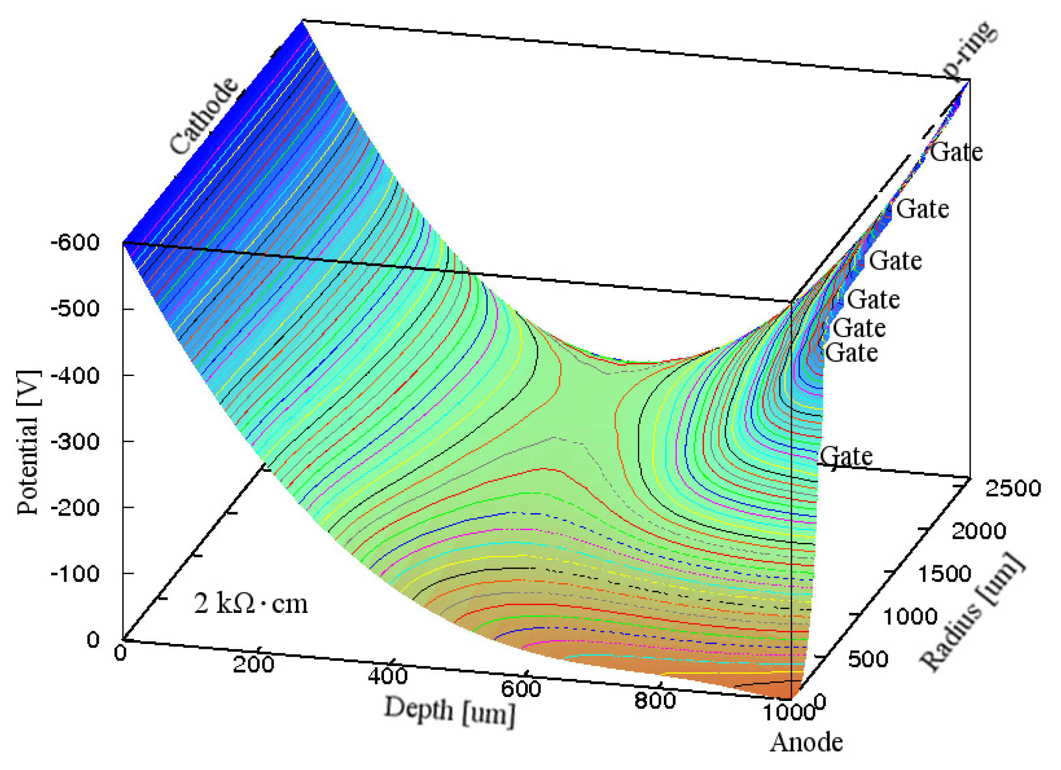
Figure 7 shows the simulated electric potential distribution for Gate D in the Si substrate inside the p-ring of the GSDD at VR of −600 V. The voltage at the saddleback was approximately −175 V. Because the average electric field toward the anode along the electric potential valley was approximately 950 V/cm, the average electron drift velocity was higher than 1 × 106 cm/s at the operating temperature (≤0 °C). This was caused by the electron mobility of 1450 cm2- V−1·s−1 in the Si substrate at room temperature [44]. This indicates that the electric field along the electric potential valley was strong enough to make all the electrons produced by the X-ray photons flow smoothly to the anode.
For a Si pin diode with dSi of 1 mm and ρSi of 2 kΩ·cm, a reverse bias of approximately −1500 V is required to deplete the whole Si layer. However, for the GSDD, a reverse bias of only −600 V was required, which is an advantage of GSDDs.
5. Conclusions
GSDDs are inexpensive Si X-ray detectors because of their simple structure. Although we have investigated GSDDs with 10-kΩ·cm Si because we have designed thicker GSDDs to detect X-ray photons with high energies, 10-kΩ·cm Si wafers are much more expensive than 2-kΩ·cm Si wafers, from which commercial SDDs are fabricated. Therefore, GSDDs with 2-kΩ·cm Si were investigated to develop low-cost X-ray detectors that can accurately detect photon counts and energies of X-ray fluorescence photons with energies of up to 35 keV. Device simulations of GSDDs with 0.5- and 1-mm-thick, 2-kΩ·cm Si substrates indicated that the X-ray detectors should work well when they are produced by using current fabrication processes. GSDDs with one gate pattern can work well for any resistivity Si substrate if the reverse bias is inversely proportional to the resistivity of the Si substrate. These findings indicate that the cost of portable X-ray fluorescence instruments can be reduced considerably.
Acknowledgements
This study was partially supported by the program “Development of System and Technology for Advanced Measurement and Analysis” of Japan Science and Technology Agency (JST).
Author Contributions
H.M. conceived and designed the device simulation; S.S performed the device simulation; Y.O. wrote the program for creating the files of input data for the device simulation; S.F., S.I., A.T. and A.H. contributed to the discussion; H.M. wrote the paper.
Conflicts of Interest
The authors declare no conflict of interest.
References
- Gatti, E.; Rehak, P. Semiconductor drift chamber—An application of a novel charge transport scheme. Nucl. Instrum. Methods 1984, 225, 608–614. [Google Scholar]
- Rehak, P.; Gatti, E.; Longoni, A.; Sampietro, M.; Holl, P.; Lutz, G.; Kemmer, J.; Prechtel, U.; Ziemann, T. Spiral silicon drift detectors. IEEE Trans. Nucl. Sci. 1989, 36, 203–209. [Google Scholar]
- Chen, W.; Kraner, H.; Li, Z.; Rehak, P.; Gatti, E.; Longoni, A.; Sampietro, M.; Holl, P.; Kemmer, J.; Faschingbauer, U. Large area cylindrical silicn drift detector. IEEE Trans. Nucl. Sci. 1992, 39, 619–628. [Google Scholar]
- Hijzen, E.A.; Schooneveld, E.M.; van Eijk, C.W.E.; Hollander, R.W. New silicon drift detector design fot diminishing lateral diffusion. Nucl. Instrum. Methods Phys. Res. 1993, 335, 271–275. [Google Scholar]
- Bertuccio, G.; Pullia, A. Room temperature X-ray spectroscopy with a silicon diode detector and an ultra low noise preamplifier. IEEE Trans. Nucl. Sci. 1994, 41, 1704–1709. [Google Scholar]
- Pinotti, E.; Longoni, A.; Gambelli, M.; Strüder, L.; Lechner, P.; Zanthier, C.V.; Kraner, C.; Kraner, H. Room temperature, high-resolution X-ray spectroscopy with silicon drift chambers. IEEE Trans. Nucl. Sci. 1995, 42, 12–16. [Google Scholar]
- Gramegna, G.; Corsi, F.; Venuto, D.; de Marzocca, C.; Vacchi, A.; Manzari, V.; Navach, F.; Beolé, S.; Casse, G.; Giubellino, P. Designing a linear silicon drift detector. IEEE Trans. Nucl. Sci. 1995, 42, 1497–1504. [Google Scholar]
- Lechner, P.; Eckbauer, S.; Hartmann, R.; Krisch, S.; Hauff, D.; Richter, R.; Soltau, H.; Strüder, L.; Fiorini, C.; Gatti, E.; et al. Silicon drift detectors for high resolution room temperature X-ray spectroscopy. Nucl. Instrum. Methods Phys. Res. 1996, 377, 346–351. [Google Scholar]
- Castoldi, A.; Rehak, P.; Holl, P. A new silicon drift detector with reduced lateral diffusion. Nucl. Instrum. Methods Phys. Res. 1996, 377, 375–380. [Google Scholar]
- Iwanczyk, J.S.; Patt, B.E.; Segal, J.; Plummer, J.; Vilkelis, G.; Hedman, B.; Hodgson, K.O.; Cox, A.D.; Rehn, L.; Metz, J. Simulation and modeling of a new silicon X-ray drift detector design for synchrotron radiation aplications. Nucl. Instrum. Methods Phys. Res. 1996, 380, 288–294. [Google Scholar]
- Gauthier, Ch.; Goulon, J.; Moguiline, E.; Rogalev, A.; Lechner, P.; Strüder, L.; Fiorini, C.; Longoni, A.; Sampietro, M.; Besch, H. A high resolution, 6 channel, silicon drift detector array with integrated JFET's designed for XAFS spectroscopy: First X-ray fluorescence excitation spectra recorded at the ESRF. Nucl. Instrum. Methods Phys. Res. 1996, 382, 524–532. [Google Scholar]
- Hartmann, R.; Strüder, L.; Kemmer, J.; Lechner, P.; Fries, O.; Lorenz, E.; Mirzoyan, R. Ultrathin entrance windows for silicon drift detectors. Nucl. Instrum. Methods Phys. Res. 1997, 387, 250–254. [Google Scholar]
- Fiorini, C.; Kemmer, J.; Lechner, P.; Kromer, K.; Rohde, M.; Schülein, T. A new detection system for X-ray microanalysis based on a silicon drift detector with Peltier cooling. Rev. Sci. Instrum. 1997, 68, 2461–2465. [Google Scholar]
- Matsuura, H.; Nishida, K. A new structure of an n-channel junction field-effect transistor embedded in a pin diode for an X-ray detector. Jpn. J. Appl. Phys. 1998, 37, L115–L118. [Google Scholar]
- Rashevsky, A.; Bonvicini, V.; Vacchi, A.; Zampa, N.; Burger, P.; Beole, S.; Idzik, M.; Petta, C.; Randazzo, N. Silicon drift detector with a continuous implanted resisitor as divider-drift electrode. Nucl. Instrum. Methods Phys. Res. 1998, 409, 210–215. [Google Scholar]
- Šonský, J.; Valk, H.; Allier, C.P.; Hollander, R.W.; van Eijk, C.W.E.; Sarro, P.M. Diminished electron cloud broadening in a silicon drift detector by sawtooth p+ strips. IEEE Trans. Nucl. Sci. 1999, 46, 53–58. [Google Scholar]
- Iwanczyk, J.S.; Patt, B.E.; Tull, C.R.; Segal, J.D.; Kenney, C.J.; Bradley, J.; Hedman, B.; Hodgson, K.O. Large area silicon drift detectors for X-rays-new results. IEEE Trans. Nucl. Sci. 1999, 46, 284–288. [Google Scholar]
- Matsuura, H.; Akatani, K.; Ueda, M.; Segawa, K.; Tomozawa, H.; Nishida, K.; Taniguchi, K. A new n-channel junction field-effect transistor embedded in the i layer of a pin diode. Jpn. J. Appl. Phys. 1999, 38, L1015–L1017. [Google Scholar]
- Strüder, L.; Meidinger, N.; Stotter, D.; Kemmer, J.; Lechner, P.; Leutenegger, P.; Soltau, H.; Eggert, F.; Rohde, M.; Schulein, T. High-resolution X-ray spectrosopy close to room temperature. Microsc. Microanal. 1999, 4, 622–631. [Google Scholar]
- Bonvicini, V.; Busso, L.; Giubellino, P.; Gregorio, A.; Idzik, M.; Kolojvari, A.; Montano, L.M.; Nouais, D.; Petta, C.; Rashevsky, A. Laboratory and test beam results from a large-area silicon drift detector. Nucl. Instrum. Methods Phys. Res. 2000, 439, 476–482. [Google Scholar]
- Hansen, K.; Tröger, L. A novel multicell silicon drift detector module for X-ray spectroscopy and imaging applications. IEEE Trans. Nucl. Sci. 2000, 47, 2748–2757. [Google Scholar]
- Fiorini, C.; Longoni, A.; Perotti, F.; Labanti, C.; Rossi, E.; Lechner, P.; Soltau, H.; Strüder, L. A monolithic array of silicon drift detectors for high-resolution gamma-ray imaging. IEEE Trans. Nucl. Sci. 2002, 49, 995–1000. [Google Scholar]
- Eggert, T.; Boslau, O.; Goldstrass, P.; Kemmer, J. Silicon drift detectors with enlarged sensitive areas. X-Ray Spectrom. 2004, 33, 246–252. [Google Scholar]
- Lechner, P.; Pahlke, A.; Soltau, H. Novel high-resolution silicon drift detectors. X-Ray Spectrom. 2004, 33, 256–261. [Google Scholar]
- Metzger, W.; Engdahl, J.; Rossner, W.; Boslau, O.; Kemmer, J. Large-area silicon drift detecotrs for new applications in nuclear medicine imaging. IEEE Trans. Nucl. Sci. 2004, 51, 1631–1635. [Google Scholar]
- Kemmer, J.; Wiest, F.; Pahlke, A.; Boslau, O.; Goldstrass, P.; Eggert, T.; Schindler, M.; Eisele, I. Epitaxy—A new technology for fabrication of advanced silicon radiatin detectors. Nucl. Instrum. Methods Phys. Res. 2005, 544, 612–619. [Google Scholar]
- Zampa, G.; Rashevsky, A.; Vacchi, A. The X-ray spectroscopic performance of a very large area silicon drift detector. IEEE Trans. Nucl. Sci. 2009, 56, 832–835. [Google Scholar]
- Carini, G.A.; Chen, W.; Geronimo, G.; de Gaskin, J.A.; Keister, J.W.; Li, Z.; Ramsey, B.D.; Rehak, P.; Siddons, D.P. Performance of a thin-window silicon drift detector X-ray fluorescence spectrometer. IEEE Trans. Nucl. Sci. 2009, 56, 2843–2849. [Google Scholar]
- Zampa, G.; Campana, R.; Feroci, M.; Vacchi, A.; Bonvicini, V.; Monte, E.D.; Evangelista, Y.; Fuschino, F.; Labanti, C.; Marisaldi, M. Room-temperature spectroscopic performance of a very-large area silicon drift detector. Nucl. Instrum. Methods Phys. Res. 2011, 633, 15–21. [Google Scholar]
- Tull, C.R.; Iwanczyk, J.S.; Patt, B.E.; Barkan, S.; Feng, L. High effeciency silicon X-ray detectors. IEEE Trans. Nucl. Sci. 2004, 51, 1803–1807. [Google Scholar]
- Parker, S.; Kenney, C.; Segal, J. 3D—A proposed new architecture for solid-state radiation detectors. Nucl. Instrum. Methods Phys. Res. 1997, 395, 328–343. [Google Scholar]
- Christophersen, M.; Phlips, B.F. Thick silicon detector. Proceedings of the IEEE Nuclear Science Symposium Conference Record, Washington, WA, USA, 19–25 October 2008; pp. 2727–2730.
- Matsuura, H.; Taniguchi, K.; Utaka, T. Radiation Detection Device. U.S. Patent Application Serial 61/185,679, 10 June 2009. [Google Scholar]
- Matsuura, H.; Taniguchi, K.; Utaka, T. Radiation Detection Device. U.S. Patent Application Serial 61/185,754, 10 June 2009. [Google Scholar]
- Matsuura, H. Silicon Carbide for Radiation Detection Devices and Radiation Detection Methods. In PCT/JP2007/65727; Japan Patent Publication 2009-022377: 19; February; 2009. [Google Scholar]
- Matsuura, H. Radiation Detection Apparatus. PCT/JP2007/65728 U.S. Patent Application 2010-0163740, 1 July 2010. [Google Scholar]
- Matsuura, H. Radiation Detection Device. U.S. Patent Application Serial 12/575,939, 8 October 2009. [Google Scholar]
- Matsuura, H.; Hullinger, D.; Taniguchi, K.; Utaka, T. Variable Ring Width SDD. U.S. Patent 8,314,468B2, 20 November 2012. [Google Scholar]
- Matsuura, H.; Takahashi, M.; Kohara, K.; Yamamoto, K.; Maeda, T.; Kagawa, Y. Simplification of structures and impruvement of sensitivity of high-energy X-rays for Si X-ray detectors (Silicon drift detetor). Denshi Joho Tsushin Gakkai Ronbunshi 2010, J93-C, 303–310. [Google Scholar]
- Matsuura, H.; Hullinger, D.; Okada, R.; Kitanoya, S.; Nishikawa, S.; Decker, K. Possibilities for thick, simple-structure silicon X-ray detectors operated by Peltier cooling. Key Eng. Mater. 2012, 495, 294–297. [Google Scholar]
- Matsuura, H.; Hullinger, D.; Decker, K.W. Simulation and fabrication of gated silicon drift X-ray detector operated by Peltier cooling. Open Electr. Electron. Eng. J. 2013, 7, 1–8. [Google Scholar]
- Matsuura, H. Simulation of thick gated silicon drift X-ray detector operated by a single high-valtage source. Jpn. J. Appl. Phys. 2013, 52. [Google Scholar] [CrossRef]
- Matsuura, H. Simulation of 1.5-mm-thick and 15-cm-diameter gated silicon drift X-ray detector operated with a single high-voltage source. Jpn. J. Appl. Phys. 2015. [Google Scholar] [CrossRef]
- Sze, S.M.; Ng, K.K. Physics of Semiconductor Devices, 3rd ed; Wiley: New York, NY, USA, 2007; pp. 790–791. [Google Scholar]
- Anderson, B.L.; Anderson, R.L. Fundamentals of Semiconductor Devices; McGraw-Hill: New York NY, USA, 2005; p. 497. [Google Scholar]


© 2015 by the authors; licensee MDPI, Basel, Switzerland. This article is an open access article distributed under the terms and conditions of the Creative Commons Attribution license ( http://creativecommons.org/licenses/by/4.0/).
Share and Cite
Matsuura, H.; Sakurai, S.; Oda, Y.; Fukushima, S.; Ishikawa, S.; Takeshita, A.; Hidaka, A. Gated Silicon Drift Detector Fabricated from a Low-Cost Silicon Wafer. Sensors 2015, 15, 12022-12033. https://doi.org/10.3390/s150512022
Matsuura H, Sakurai S, Oda Y, Fukushima S, Ishikawa S, Takeshita A, Hidaka A. Gated Silicon Drift Detector Fabricated from a Low-Cost Silicon Wafer. Sensors. 2015; 15(5):12022-12033. https://doi.org/10.3390/s150512022
Chicago/Turabian StyleMatsuura, Hideharu, Shungo Sakurai, Yuya Oda, Shinya Fukushima, Shohei Ishikawa, Akinobu Takeshita, and Atsuki Hidaka. 2015. "Gated Silicon Drift Detector Fabricated from a Low-Cost Silicon Wafer" Sensors 15, no. 5: 12022-12033. https://doi.org/10.3390/s150512022
APA StyleMatsuura, H., Sakurai, S., Oda, Y., Fukushima, S., Ishikawa, S., Takeshita, A., & Hidaka, A. (2015). Gated Silicon Drift Detector Fabricated from a Low-Cost Silicon Wafer. Sensors, 15(5), 12022-12033. https://doi.org/10.3390/s150512022