4.1. Experiment Process and Results
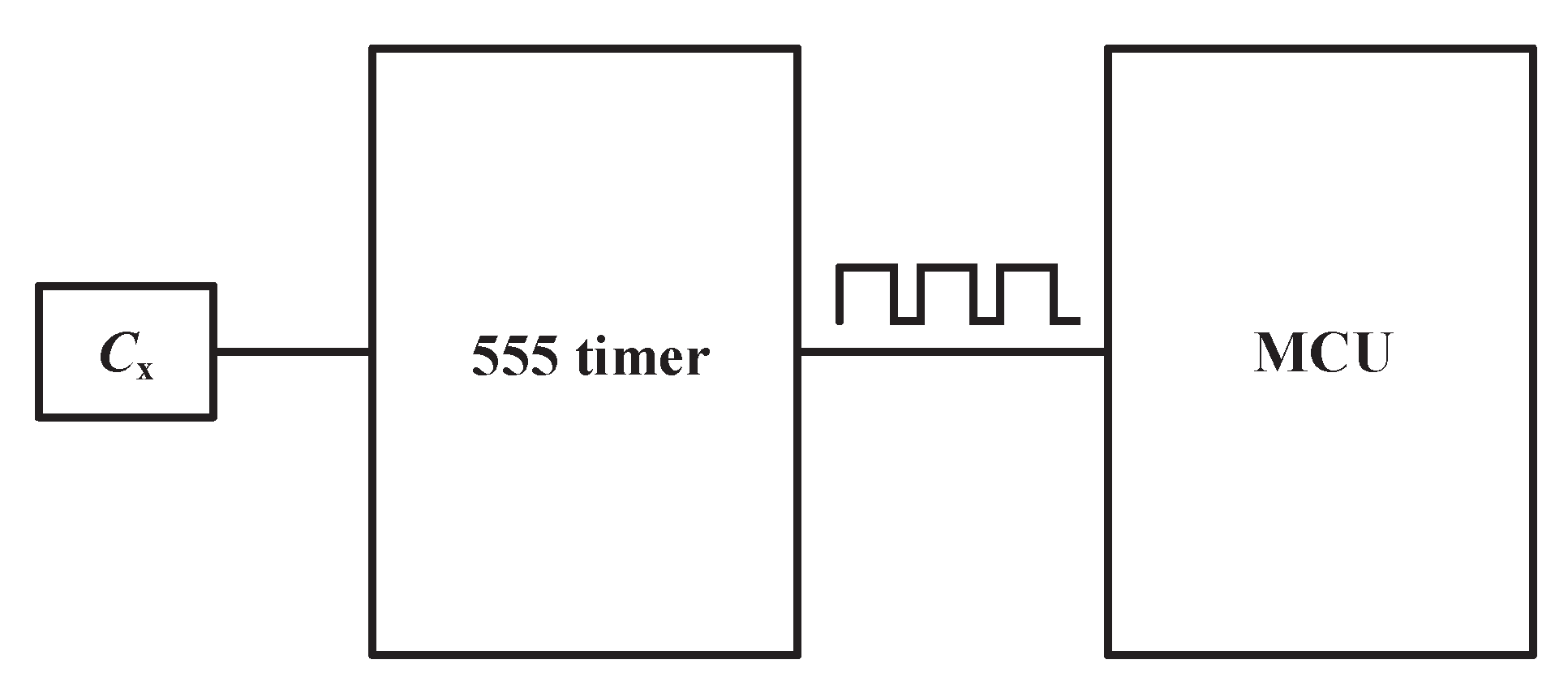
A low-cost method that can fulfill the requirements of the application and detection accuracy was adopted. The measurement circuit is showed in
Figure 9. The system consists of two major chips, 555 timer and Microcontroller Unit (MCU).
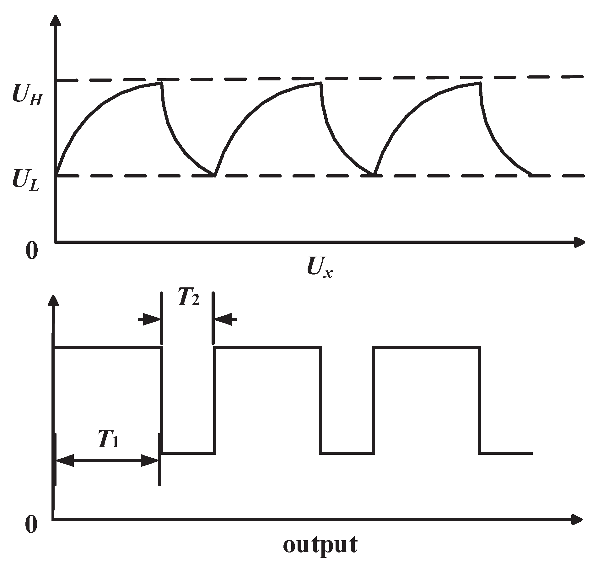
C is the capacitance to be measured. When power is on, the output of 555 timer is a square-wave signal. The period of the square-wave signal
T is in proportion to
C. The working process of the circuit can be divided into two parts: (a) first, when the circuit is powered, the capacitor
C has not been charged. The voltage of the capacitor
U is lower than reference low voltage
U, the output is high. Then,
U is charged by power supply through
R and
R, so
U increases exponentially. When
U rises to reference high voltage
U, the output is low, and the capacitor starts to discharge. The time of
U rising from
U to
U is
T:
(b) Second, Capacitor
C discharges by
R, so
U declines. When
U drops to
U, the output is high. The time of
U droping from
U to
U is
T:
Then, the circuit repeats process (a) and (b). Output of the 555 timer will generate a square wave, and the period of output is
T:
The output of the 555 timer is directly connected to a microcontroller’s T0 port and microcontroller’s timer0 counts for T0. By counting for a T0 port in a known fixed time and checking the count value, the period
T can be computed. As the value of
T,
R and
R is known, and the capacitance to be measured is easy to work out according to Equation (
4).
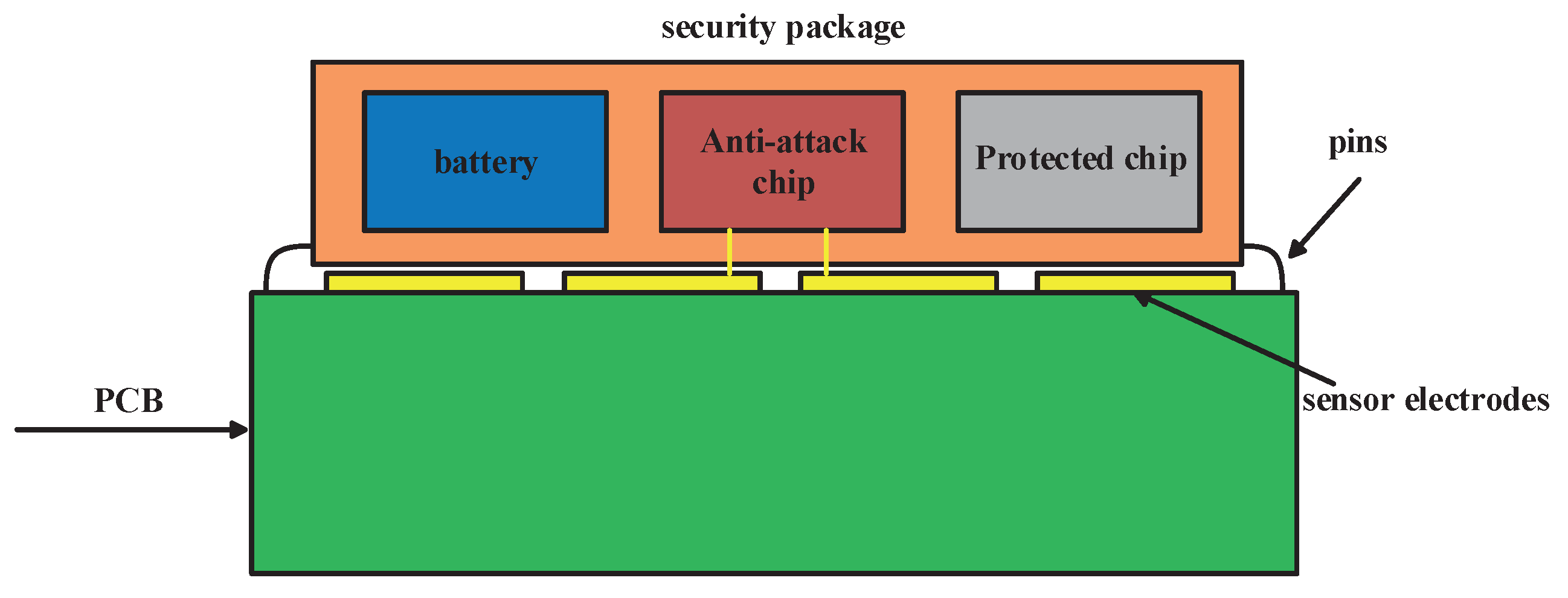
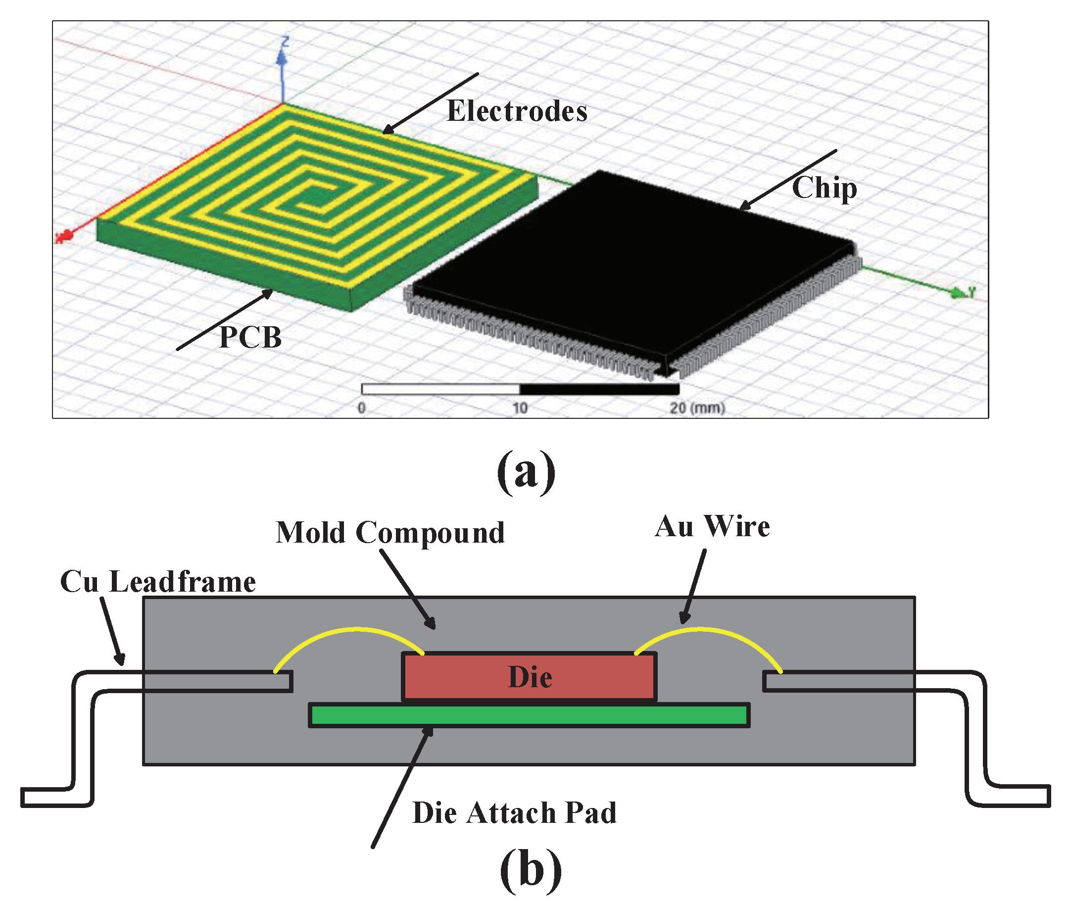
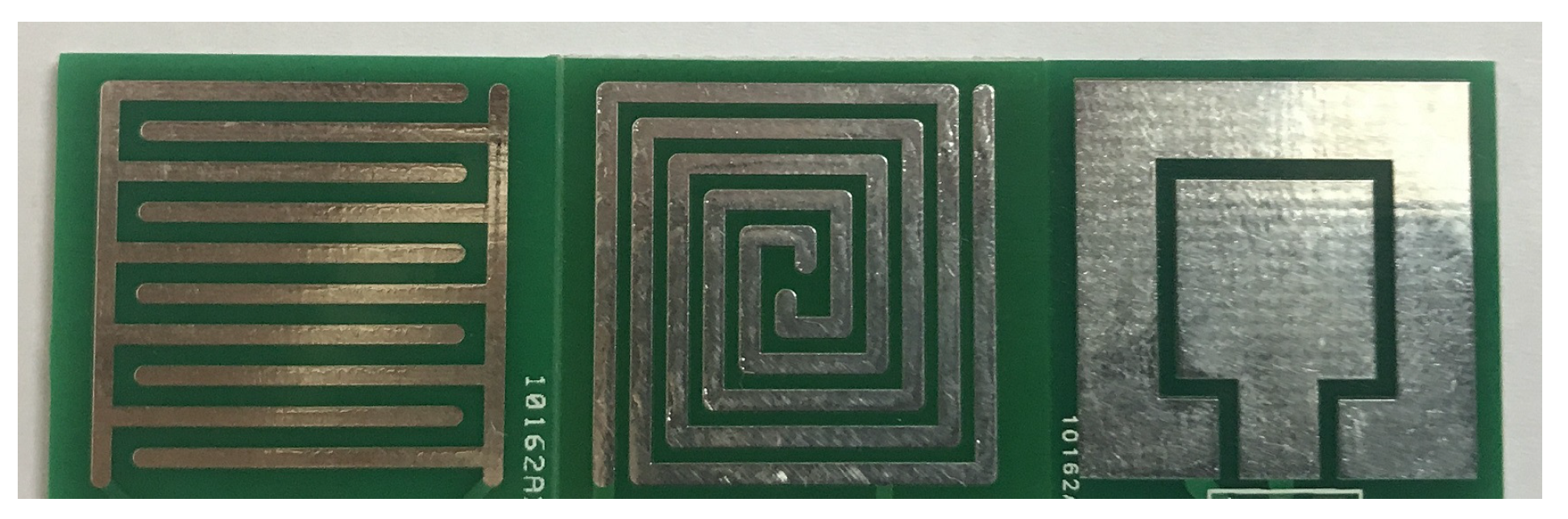
In order to verify the conclusions from simulation, fringing electric field sensors were fabricated. A photograph of prototype sensors is shown in
Figure 11. All of these capacitive sensors were manufactured using a two-layer PCB process. The capacitive sensors’ pattern, electrodes’ width and spacing were consistent with simulation to ensure its credibility. Firstly, FEF sensor was connected to a 555 timer and the chip to be protected was placed on the FEF sensor. The output of a 555 timer generated square wave and a microcontroller counted for it in a fixed time. The count value was displayed by a microcontroller’s output pins. According to Equation (
4), FEF sensor’s capacitance when the chip was on the sensor was computed. Then, the chip to be protected was taken off of the FEF sensor and the sensor’s capacitance was computed in the same way. Finally, a sensor’s capacitance change can be easily obtained.
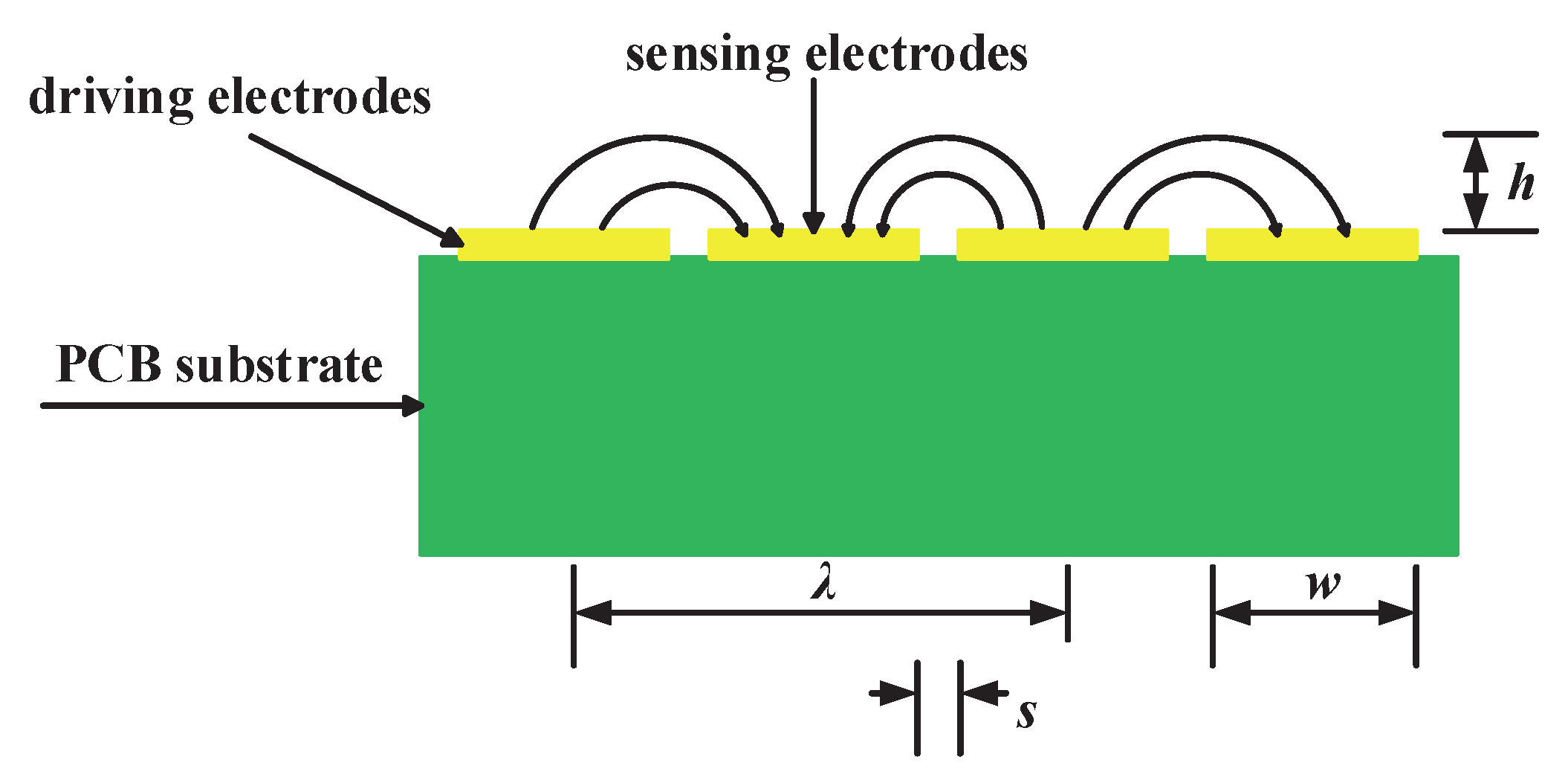
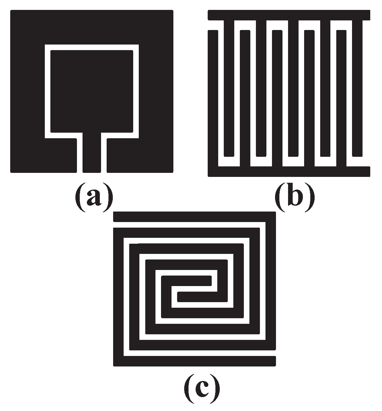
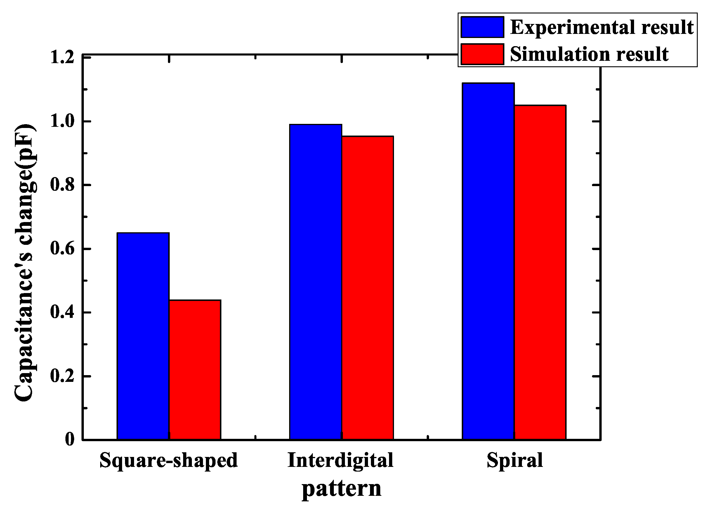
So as to ensure the consistency between simulation and experiment, all parameters of the sensors were equal to models of simulation. Firstly, three fringing electric field sensors of different patterns in
Figure 5 were manufactured and the capacitance was measured using the circuit of
Figure 9. The result of measurement is shown in
Figure 12. The parameters of FEF sensors in
Figure 12 are shown in
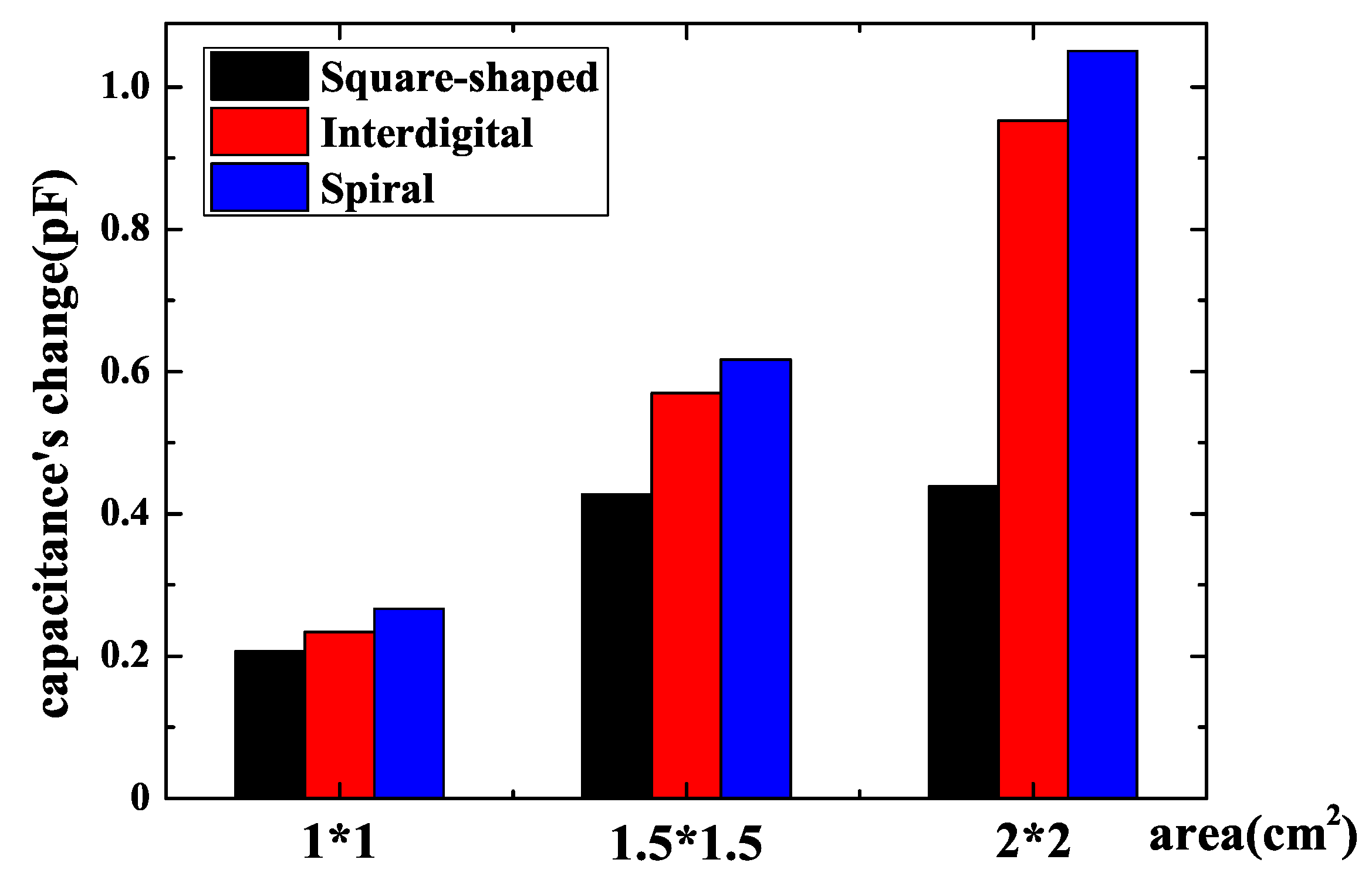
Table 3. The capacitance’s change of a square-shaped pattern, interdigital pattern and spiral pattern in experiments are 0.65 pF, 0.99 pF and 1.12 pF. It can be seen that the results corresponded to simulation. The spiral pattern is the best structure among three patterns, while the interdigital pattern are better than a square-shaped pattern. Experimental results show that the spiral pattern is the most suitable sensor pattern for protecting the chip at system-level protection.
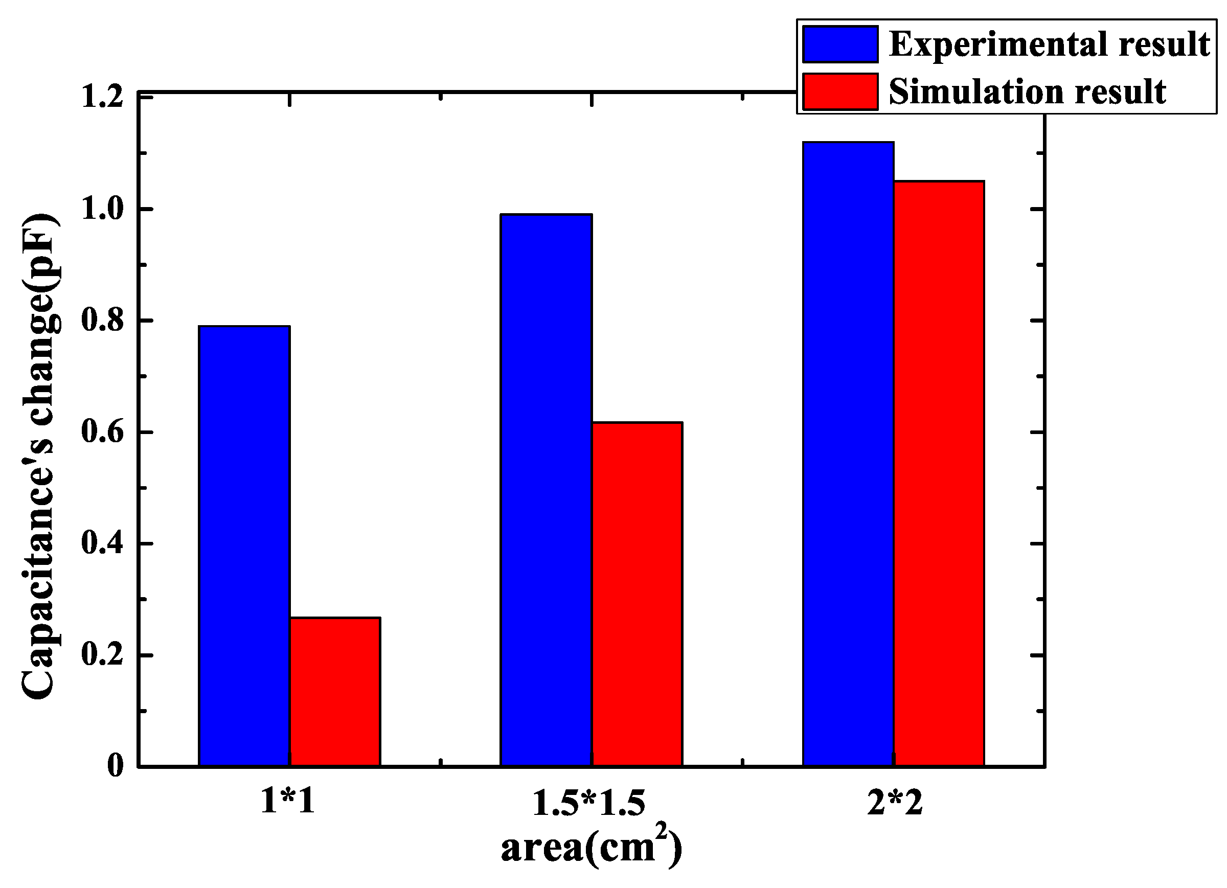
As the best pattern for sensors was determined, experiments with different sensors’ areas were carried out. Measurement of a spiral pattern fringing electric field sensor with an area of 2 cm × 2 cm, 1.5 cm × 1.5 cm and 1 cm × 1 cm consistent with simulation was done and the results are presented in
Figure 13. The parameters of FEF sensors in
Figure 13 are shown in
Table 4. The capacitance’s change of these sensors with three different areas in experiments are respectively 0.79 pF, 0.99 pF and 1.12 pF. It is shown that the capacitance’s change gets larger when a sensor’s area gets larger. Consequently, in order to maximize capacitance’s change, the area of a sensor should be equal to the chip’s area. However, as what has been discussed, a large sensor means area for routing is reduced. If area for routing is essential, a small sensor can be made as long as capacitance change of a small sensor can be distinguished by a subsequent circuit.
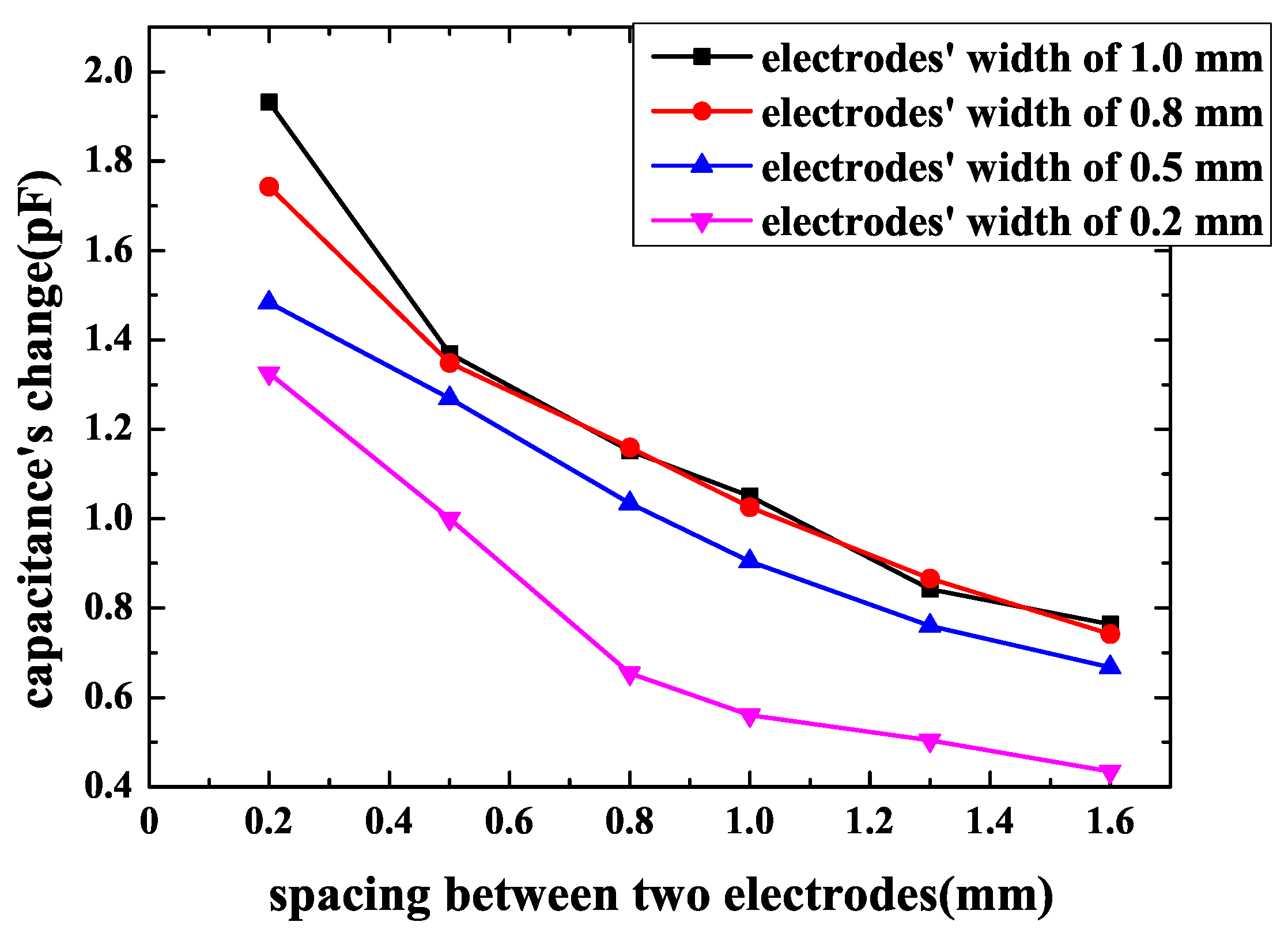
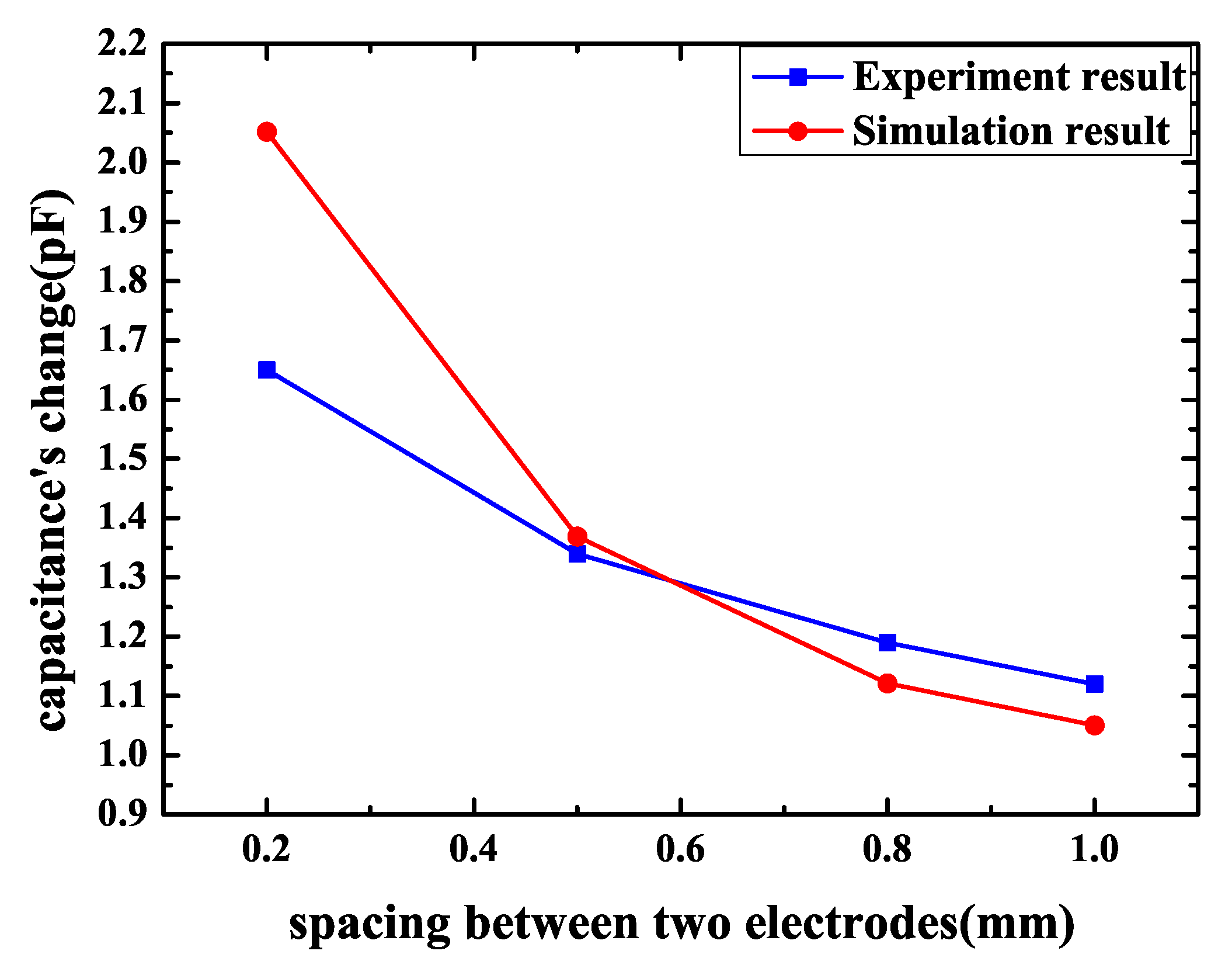
As what has been discussed before, the best pattern and area were determined. Geometrical parameters’ influence should also be confirmed. Firstly, the influence of spacing between two electrodes was measured. The parameters were equal to simulation that the electrodes’ width was 1 mm and the spacing between two electrodes ranged from 0.2–1.0 mm. The sensor’s pattern was spiral and the area was equal to the chip of 2 cm × 2 cm. The result is shown in
Figure 14. The parameters of FEF sensors in
Figure 14 are shown in
Table 5. When spacing becomes smaller, capacitance’s change increases. This phenomenon is consistent with simulation. When spacing changes from 0.2–1.0 mm, capacitance’s change increases by 0.53 pF. Thus, small spacing between two electrodes should be a better choice for bigger capacitance’s change.
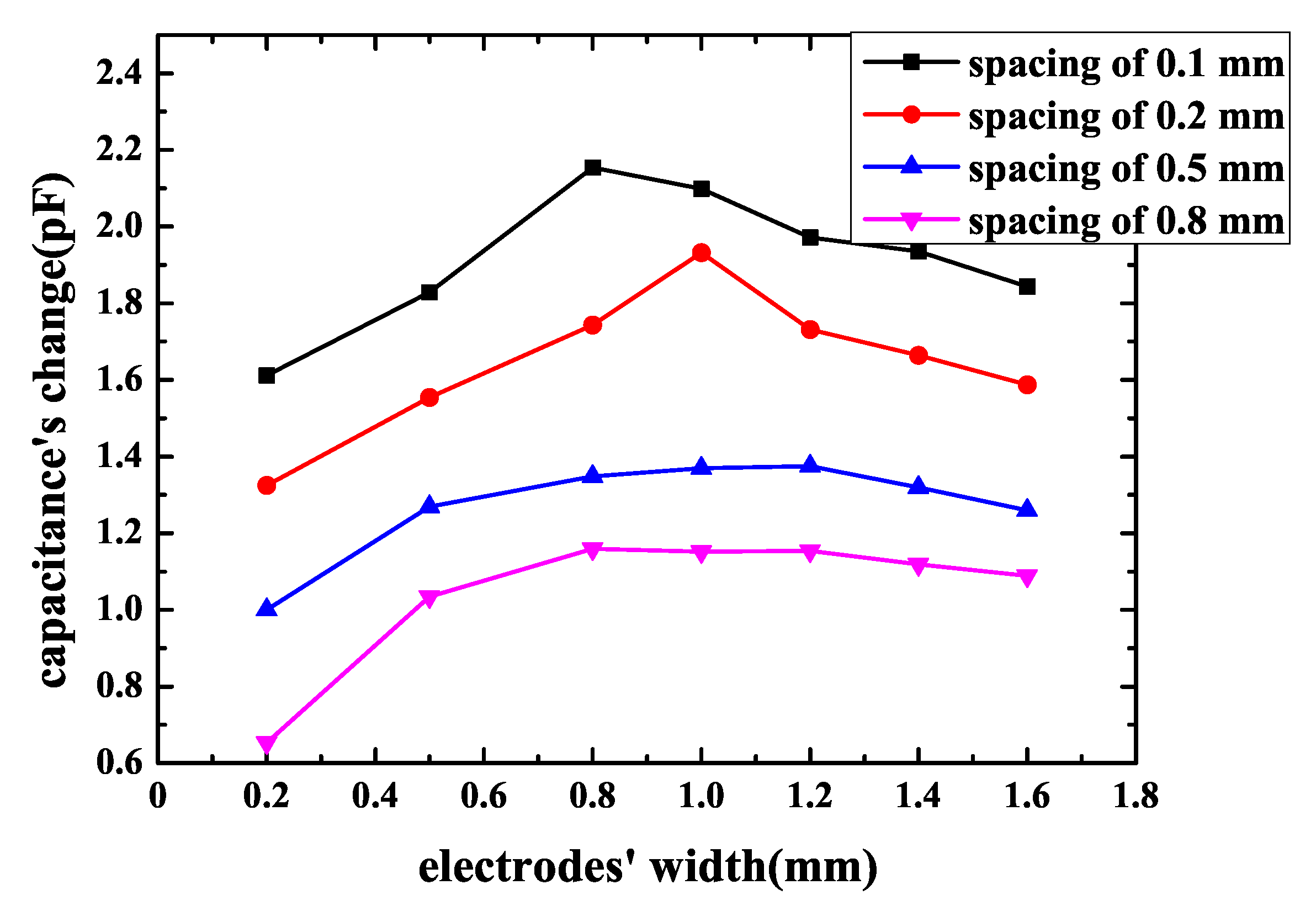
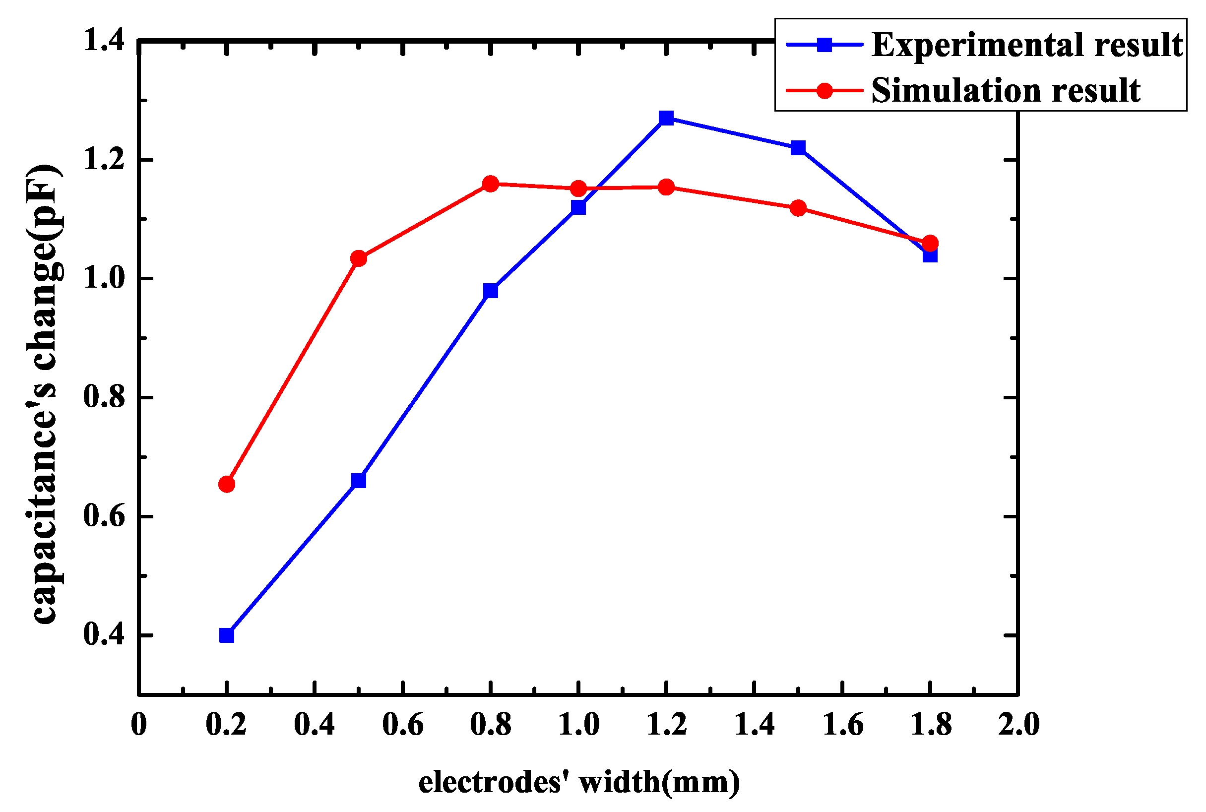
Then, the influence of electrodes’ width is measured. The spacing is 0.8 mm and electrodes’ width varies from 0.2–1.8 mm. The result of experiment is shown in
Figure 15. The parameters of FEF sensors in
Figure 15 are shown in
Table 6. It can be noticed that, as electrodes’ width gets bigger, a sensor’s capacitance change gets bigger at first, when electrodes’ width reaches the best width, capacitance’s change reaches a maximum value, then as width gets bigger, capacitance’s change gets smaller. The best electrodes’ width for the chip in this paper is 1.2 mm. For the anti-attack fringing electric field sensor, the capacitance is not just determined by the sensor’s pattern and size, it is also influenced by the geometrical parameters of the sensor to a great extent. On the whole, the results of measurement correspond to the simulation models’ predictions pretty well.
4.2. Discussion
On the whole, the experimental results are in accordance with simulation results. As sensor’s patterns, areas and geometrical parameters change, experimental results and simulation results present the same trend. However, the concrete value of capacitance’s change is different. The reason is that a simulation model’s component of the chip is too simple. The real chip’s component is much more complex, so a real chip’s dielectric constant is different from a simulation model’s dielectric constant. Furthermore, when electrodes’ width and spacing are below 0.5 mm, simulation accuracy drops, so there are distinct differences between simulation results and experimental results. There are also instrumental errors and sensors manufacturing errors may also have been present in the experiment.
According to simulation and experiments, the optimal design method is as summarized below. Spiral pattern is the best because the overall sensor sensitivity is proportional to the effective electrode length [
25]. The spiral pattern was designed in order to maximize its effective electrode length. For sensors with the same area, the sensor that has a complex pattern has greater effective electrode length and consequently has a much higher sensitivity. Among these three patterns, the spiral pattern sensor has the biggest effective electrode length and has the biggest capacitance’s change. Consequently, a complex pattern with long effective electrode length is a good choice.
The reason for a larger sensor with larger capacitance’s change is that the sensor’s sensitivity is proportional to both effective electrode length and the electrode area [
25]. For the sensor with the same electrodes’ width and spacing, when the sensor’s area get bigger, its electrodes area get bigger and the sensor can contain more electrodes, which means it has longer effective electrode length. As a result, as what is shown in
Figure 13, the sensor’s capacitance change is proportional to the sensor’s area. The biggest possible area of sensor is equal to the area of the chip to be protected.
For a certain electrodes’ width, the capacitance’s change of sensor becomes greater as spacing between two electrodes gets smaller. The reason is that when spacing decreases, total capacitance of the FEF sensor increases and the capacitance’s change caused by the chip to be protected becomes larger accordingly. According to simulation and measurement, spacing’s influence is more obvious and important than electrode width’s influence. When electrodes’ width is fixed and spacing decreases from 1–0.2 mm, capacitance’s change increases distinctly. To improve sensor’s sensitivity, spacing should be small. However, for a certain spacing between two electrodes, the sensor has the best electrodes’ width. The reason is that, as mentioned in
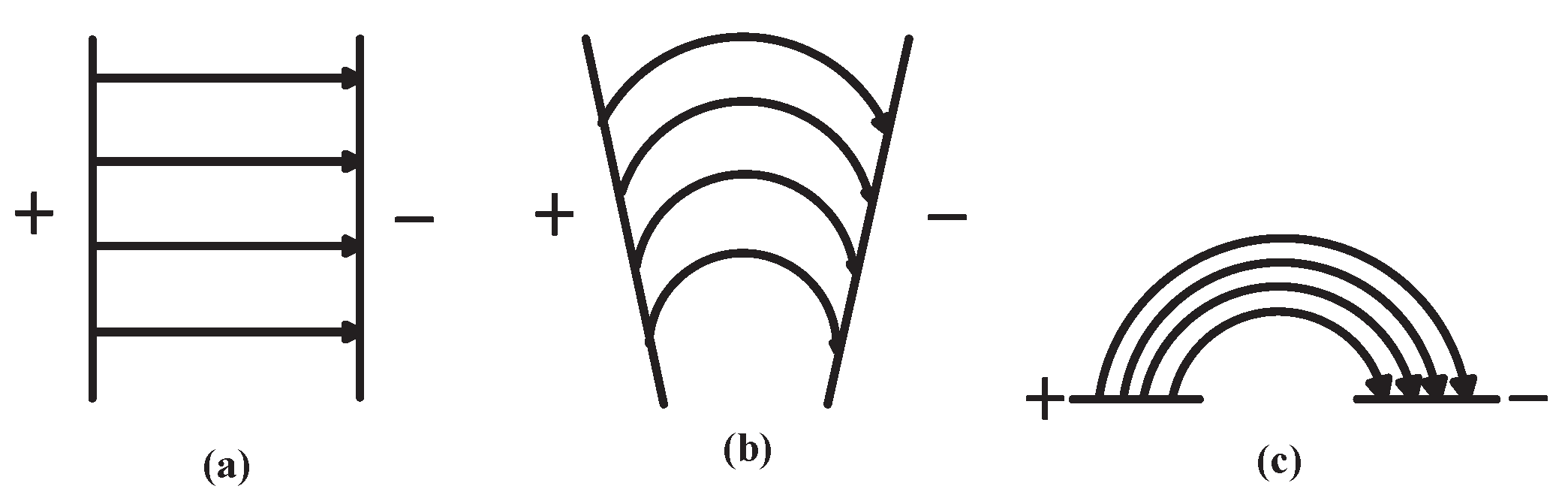
Section 2, penetration depth of the fringing electric field sensors’ electric field line is proportional to the length of
, which is the distance between the centerlines of the two adjacent driving or sensing electrodes. Penetration depth has an influence on sensor’s measurement range and capacitance’s magnitude, and, when penetration depth increases, the electric field line can reach a farther distance; therefore, the FEF sensor’s measurement range increases [
16]. However, penetration depth’s incremental results in sensor’s capacitance magnitude’s decreases. As a result, capacitance’s change caused by the chip to be protected may reduce. According to what has been discussed above, there is a best penetration depth, while penetration depth is dependent on the distance between the centerline of the two same adjacent electrodes, which is equal to two times the sum of electrode width and electrode spacing. Penetration depth is determined by the sum of electrode width and electrode spacing. A best electrode width exists. In other words, the best sum of electrode width and electrode spacing exists. As a consequence, for a certain spacing, the sensor has the best electrodes’ width. The best electrodes’ width should be determined based on the actual situation. However, spacing’s impact is significant and it is greater than the impact of electrodes’ width. As long as spacing decreases, capacitance change of the sensor increases. The effect of electrodes’ width is less pronounced, and the best electrodes’ width is when spacing is constant.
Generally, errors in fringing electric field sensors measurement system come from sources such as the environment conditions, accuracy of sensor manufacturing and the instrumentation errors. However, measurement results were quite stable and reliable. It can be seen from simulation and measurement that the fringing electric field sensor is fit and can be useful in an information security field. It can be used to accurately detect whether a chip is dismantled from PCB at system-level protection. In this paper, the qualitative analysis was mainly made because, as mentioned in
Section 1, a fringing electric field sensor is difficult to be analyzed due to its nonlinear feature. Research was mostly done through simulation and experiments at present. Quantitative analysis is the goal of future research.


