Carbon-Based Electrode Materials for Microsupercapacitors in Self-Powering Sensor Networks: Present and Future Development

 , , ,
, , ,  , and
, and 
Abstract
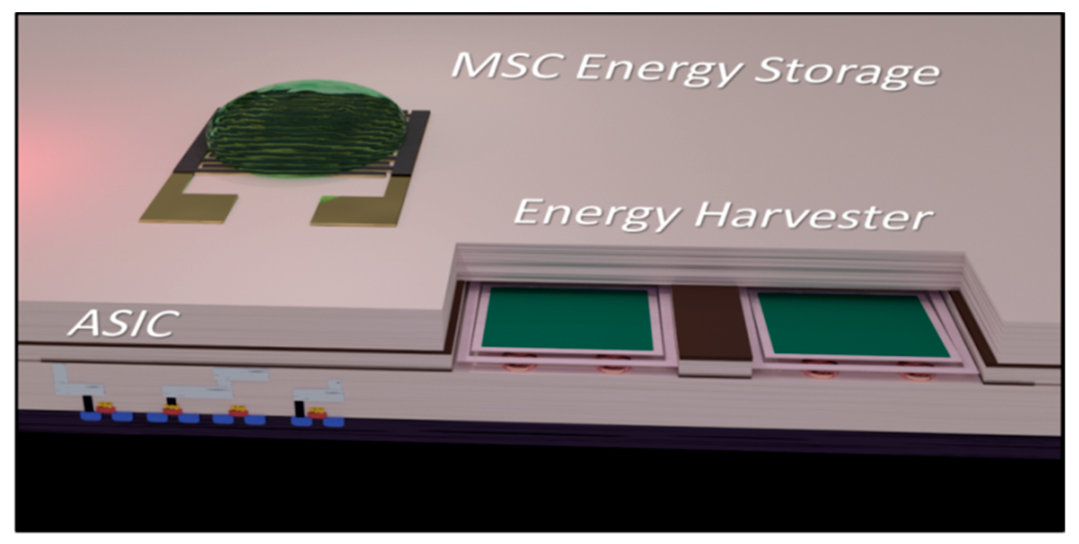
:1. Introduction
2. Materials and Methods
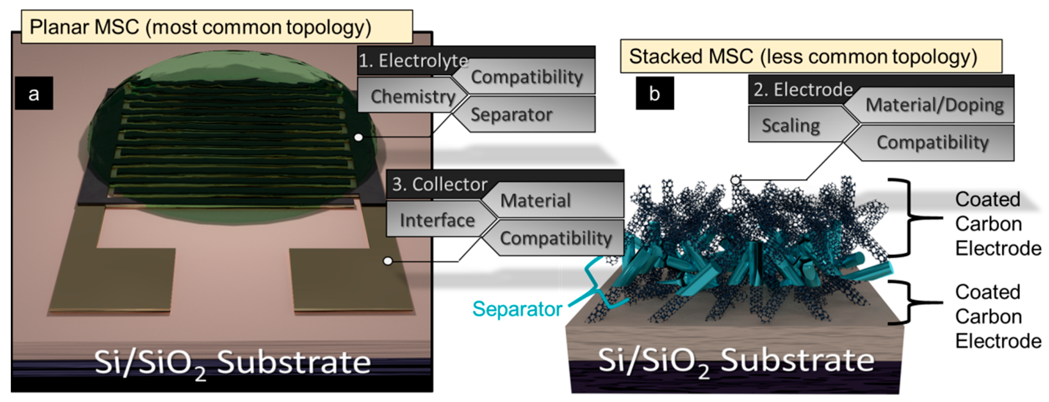
2.1. Planar Microsupercapacitor Fabrication
2.2. Electrode Materials
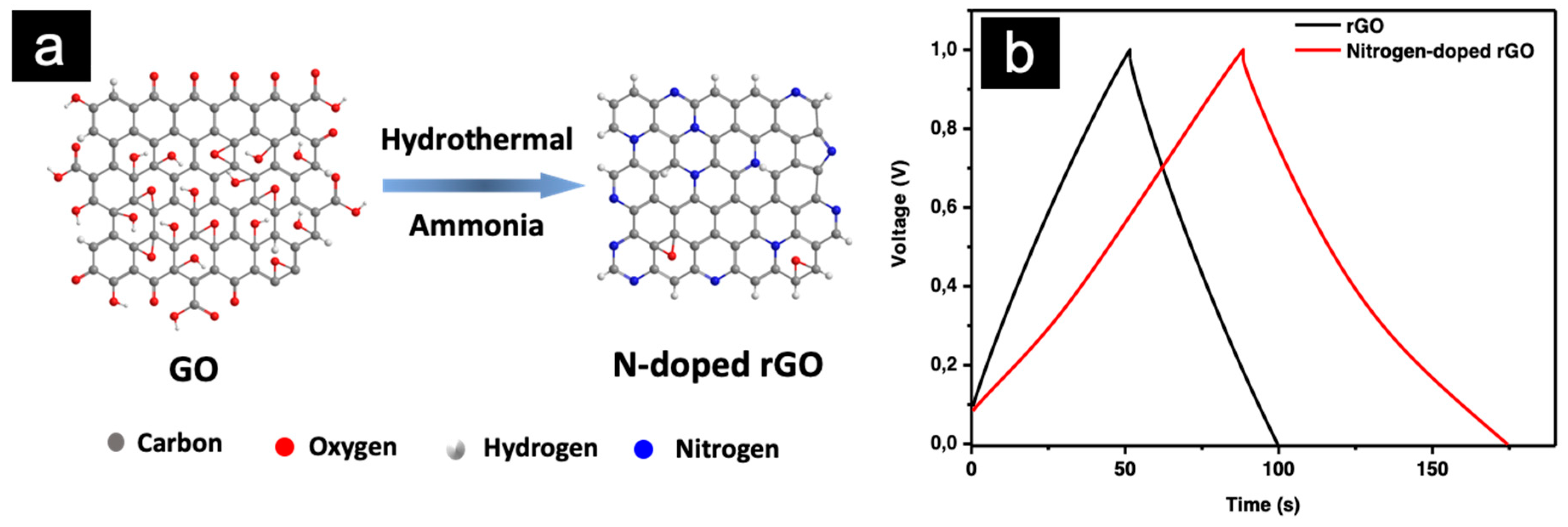
2.2.1. Graphene Oxide (GO)
2.2.2. Carbon Nanotubes (CNTs)
2.2.3. Vertical Graphene (VG)
3. Results
3.1. Electrode Adhesion
3.2. Electrode Doping for Performance Enhancement
3.3. Geometric Scaling of Electrodes
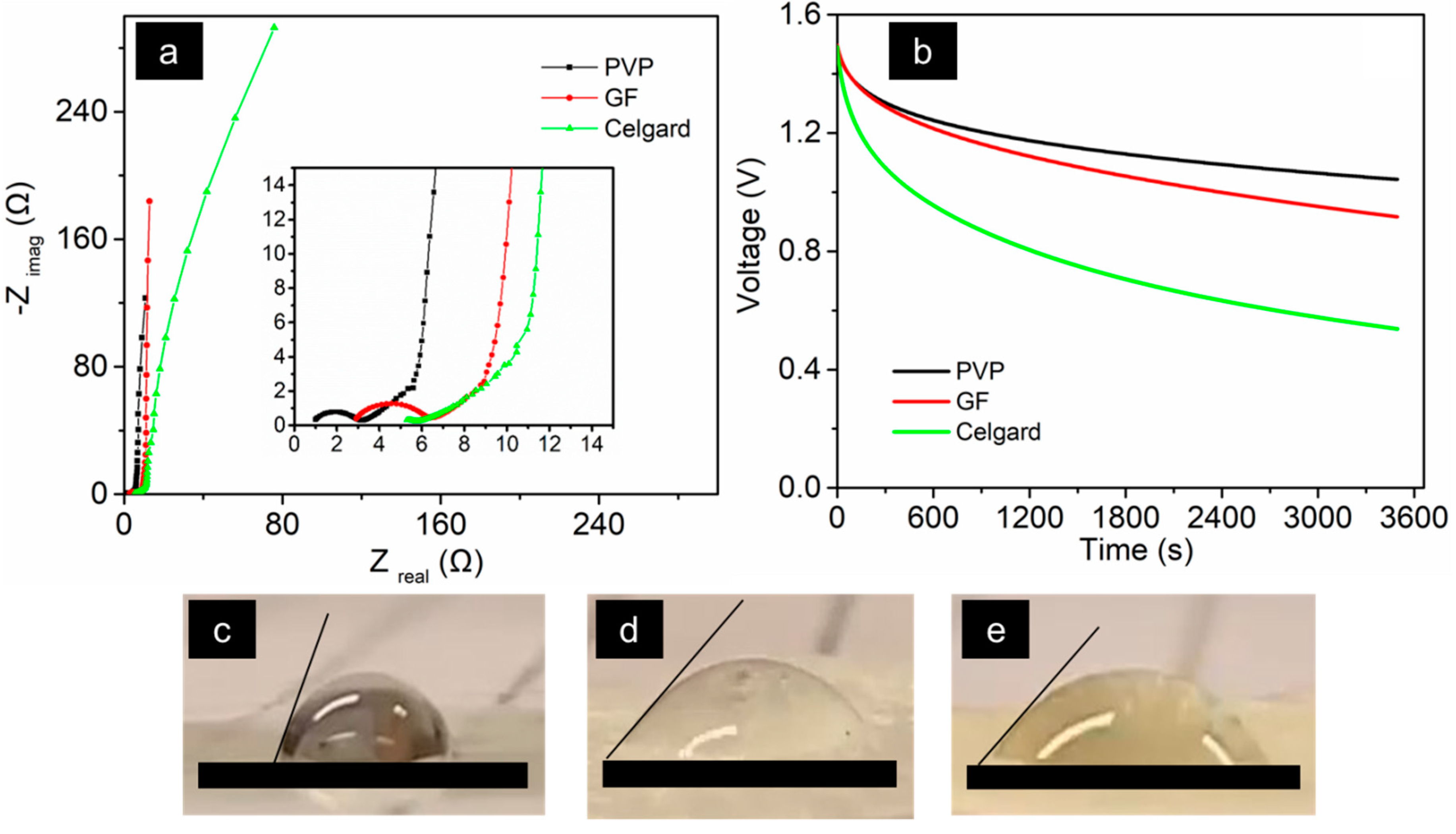
3.4. Separator Considerations for Stacked MSC Configurations
- Thickness: It should be as thin as possible without compromising mechanical stability or electrical reliability.
- Chemical stability: It should not react with the electrodes or the electrolyte under any circumstances. Otherwise, separator membrane degradation will compromise the reliability of the MSC device.
- Porosity: Porosity determines the amount of electrolyte the separator can hold in its pores to facilitate better ionic conductivity. At the same time, a highly porous separator might degrade under the influence of electrolytes. The standard porosity of typical separators is about 40%.
- Pore Size: Pore size should be in accordance with the pore size of the electrodes. For better performance, the ion size of the electrolytes should also be taken into account. In practice, separator membranes with sub-micron pore size are sufficient.
- Wettability: The separator should be easily wetted by aqueous electrolyte (hydrophilic) or non-aqueous electrolyte (hydrophobic) and should reliably hold the electrolyte for a very long time.
- Permeability: The presence of the separator should not influence the characteristics of the electrolyte. The loss of ionic conductivity can be expressed with a parameter called the Macmulin number. This is calculated as the ratio between the resistance of electrolyte in presence of a separator and the resistance of a pristine electrolyte. The Macmulin number of practical separators is of the order 10–12. Homogeneous composition of the separator material is also important to achieve an improved permeability.
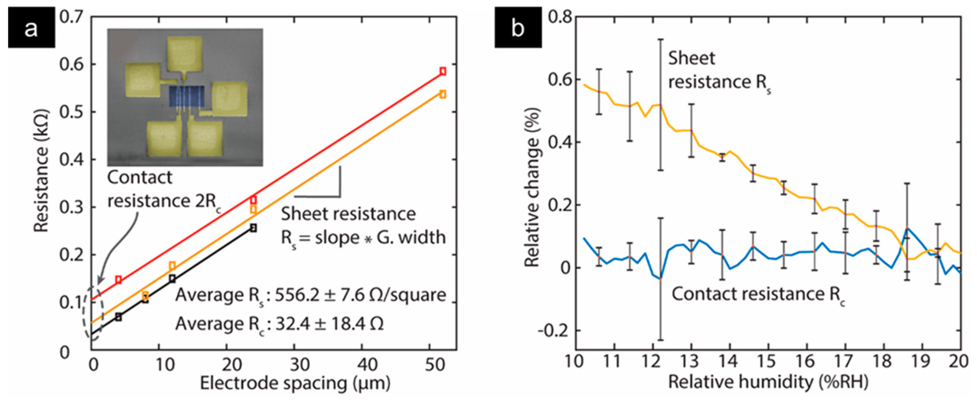
3.5. Electrode/Current Collector Contact Resistance
4. Discussion
5. Conclusions
Author Contributions
Funding
Conflicts of Interest
References
- Mack, C.A. Fifty years of Moore’s law. IEEE Trans. Semicond. Manuf. 2011, 24, 202–207. [Google Scholar] [CrossRef]
- Waldrop, M.M. The chips are down for Moore’s law. Nat. News 2016, 530, 144. [Google Scholar] [CrossRef] [PubMed]
- Dreslinski, R.G.; Wieckowski, M.; Blaauw, D.; Sylvester, D.; Mudge, T. Near-threshold computing: Reclaiming moore’s law through energy efficient integrated circuits. Proc. IEEE 2010, 98, 253–266. [Google Scholar] [CrossRef]
- Schaller, R.R. Moore’s law: past, present and future. IEEE Spectr. 1997, 34, 52–59. [Google Scholar] [CrossRef]
- Yeric, G. Moore’s law at 50: Are we planning for retirement? In Proceedings of the IEEE International Electron Devices Meeting (IEDM), Washington, DC, USA, 7–9 December 2015; p. 1. [Google Scholar]
- Smith, A. Graphene-based devices for more than Moore applications. Ph.D. Thesis, KTH Royal Institute of Technology, Stockholm, Sweden, 2016. [Google Scholar]
- Bataillou, J.; Coster, D.J.; Peterson, C.R.; Raff, J.; Stringer, C.J. Battery for a portable display device. U.S. Patent 29/473,939, 2014. [Google Scholar]
- Sato, J.; Suzuki, S. Battery for portable computer. U.S. Patent 29/445,041, 2013. [Google Scholar]
- Lin, P. Rechargeable battery device. U.S. Patent 29/502,986, 2016. [Google Scholar]
- Goodenough, J.B.; Park, K.S. The Li-ion rechargeable battery: A perspective. J. Am. Chem. Soc. 2013, 135, 1167–1176. [Google Scholar] [CrossRef] [PubMed]
- Gallo, A.B.; Simões-Moreira, J.R.; Costa, H.K.M.; Santos, M.M.; dos Santos, E.M. Energy storage in the energy transition context: A technology review. Renew. Sustain. Energy Rev. 2016, 65, 800–822. [Google Scholar] [CrossRef]
- Dubal, D.P.; Chodankar, N.R.; Kim, D.H.; Gomez-Romero, P. Towards flexible solid-state supercapacitors for smart and wearable electronics. Chem. Soc. Rev. 2018, 47, 2065–2129. [Google Scholar]
- Lu, X.; Yu, M.; Wang, G.; Tong, Y.; Li, Y. Flexible solid-state supercapacitors: design, fabrication and applications. Energy Environ. Sci. 2014, 7, 2160–2181. [Google Scholar] [CrossRef]
- Dong, L.; Xu, C.; Li, Y.; Huang, Z.H.; Kang, F.; Yang, Q.H.; Zhao, X. Flexible electrodes and supercapacitors for wearable energy storage: A review by category. J. Mater. Chem. A 2016, 4, 4659–4685. [Google Scholar] [CrossRef]
- Fu, Y.; Cai, X.; Wu, H.; Lv, Z.; Hou, S.; Peng, M.; Yu, X.; Zou, D. Fiber supercapacitors utilizing pen ink for flexible/wearable energy storage. Adv. Mater. 2012, 24, 5713–5718. [Google Scholar] [CrossRef]
- Meng, Y.; Zhao, Y.; Hu, C.; Cheng, H.; Hu, Y.; Zhang, Z.; Shi, G.Q.; Qu, L. All-graphene core-sheath microfibers for all-solid-state, stretchable fibriform supercapacitors and wearable electronic textiles. Adv. Mater. 2013, 25, 2326–2331. [Google Scholar] [CrossRef] [PubMed]
- Shen, C.; Xu, S.; Xie, Y.; Sanghadasa, M.; Wang, X.; Lin, L. A review of on-chip micro supercapacitors for integrated self-powering systems. J. Microelectromech. Syst. 2017, 26, 949–965. [Google Scholar] [CrossRef]
- Roundy, S.; Wright, P.K.; Rabaey, J.M. Energy Scavenging for Wireless Sensor Networks; Springer: Berlin/Heidelberg, Germany, 2003; pp. 45–47. [Google Scholar]
- Paradiso, J.A.; Starner, T. Energy scavenging for mobile and wireless electronics. IEEE Pervasive Comput. 2005, 4, 18–27. [Google Scholar] [CrossRef]
- Wang, Z.L. Towards self-powered nanosystems: From nanogenerators to nanopiezotronics. Adv. Funct. Mater. 2008, 18, 3553–3567. [Google Scholar] [CrossRef]
- Schmuch, R.; Wagner, R.; Hörpel, G.; Placke, T.; Winter, M. Performance and cost of materials for lithium-based rechargeable automotive batteries. Nat. Energy 2018, 3, 267. [Google Scholar] [CrossRef]
- Wang, Y.; Song, Y.; Xia, Y. Electrochemical capacitors: Mechanism, materials, systems, characterization and applications. Chem. Soc. Rev. 2016, 45, 5925–5950. [Google Scholar] [CrossRef] [PubMed]
- Li, B.; Dai, F.; Xiao, Q.; Yang, L.; Shen, J.; Zhang, C.; Cai, M. Nitrogen-doped activated carbon for a high energy hybrid supercapacitor. Energy Environ. Sci. 2016, 9, 102–106. [Google Scholar] [CrossRef]
- Liu, C.; Zhang, C.; Song, H.; Zhang, C.; Liu, Y.; Nan, X.; Cao, G. Mesocrystal MnO cubes as anode for Li-ion capacitors. Nano Energy 2016, 22, 290–300. [Google Scholar] [CrossRef] [Green Version]
- Ding, J.; Hu, W.; Paek, E.; Mitlin, D. Review of hybrid ion capacitors: From aqueous to lithium to sodium. Chem. Rev. 2018, 118, 6457–6498. [Google Scholar] [CrossRef]
- Du Pasquier, A.; Plitz, I.; Gural, J.; Badway, F.; Amatucci, G.G. Power-ion battery: Bridging the gap between Li-ion and supercapacitor chemistries. J. Power Sources 2004, 136, 160–170. [Google Scholar] [CrossRef]
- Cericola, D.; Kötz, R. Hybridization of rechargeable batteries and electrochemical capacitors: Principles and limits. Electrochim. Acta 2012, 72, 1–17. [Google Scholar] [CrossRef]
- Dubal, D.P.; Ayyad, O.; Ruiz, V.; Gomez-Romero, P. Hybrid energy storage: The merging of battery and supercapacitor chemistries. Chem. Soc. Rev. 2015, 44, 1777–1790. [Google Scholar] [CrossRef] [PubMed]
- Zuo, W.; Li, R.; Zhou, C.; Li, Y.; Xia, J.; Liu, J. Battery-supercapacitor hybrid devices: Recent progress and future prospects. Adv. Sci. 2017, 4, 1600539. [Google Scholar] [CrossRef]
- Raza, W.; Ali, F.; Raza, N.; Luo, Y.; Kim, K.H.; Yang, J.; Kumar, S.; Mehmood, A.; Kwon, E.E.; Kumar, S.; et al. Recent advancements in supercapacitor technology. Nano Energy 2018, 52, 441–473. [Google Scholar] [CrossRef]
- Zhong, C.; Deng, Y.; Hu, W.; Qiao, J.; Zhang, L.; Zhang, J. A review of electrolyte materials and compositions for electrochemical supercapacitors. Chem. Soc. Rev. 2015, 44, 7484–7539. [Google Scholar] [CrossRef] [PubMed]
- Wang, G.; Zhang, L.; Zhang, J. A review of electrode materials for electrochemical supercapacitors. Chem. Soc. Rev. 2012, 41, 797–828. [Google Scholar] [CrossRef] [Green Version]
- Zhi, M.; Xiang, C.; Li, J.; Li, M.; Wu, N. Nanostructured carbon–metal oxide composite electrodes for supercapacitors: A review. Nanoscale 2013, 5, 72–88. [Google Scholar] [CrossRef] [PubMed]
- González, A.; Goikolea, E.; Barrena, J.A.; Mysyk, R. Review on supercapacitors: Technologies and materials. Renew. Sustain. Energy Rev. 2016, 58, 1189–1206. [Google Scholar] [CrossRef]
- Wang, F.; Wu, X.; Yuan, X.; Liu, Z.; Zhang, Y.; Fu, L.; Zhu, Y.; Zhou, Q.; Wu, Y.; Huang, W. Latest advances in supercapacitors: From new electrode materials to novel device designs. Chem. Soc. Rev. 2017, 46, 6816–6854. [Google Scholar] [CrossRef] [PubMed]
- Borenstein, A.; Hanna, O.; Attias, R.; Luski, S.; Brousse, T.; Aurbach, D. Carbon-based composite materials for supercapacitor electrodes: A review. J. Mater. Chem. A 2017, 5, 12653–12672. [Google Scholar] [CrossRef]
- Wang, Q.; Yan, J.; Fan, Z. Carbon materials for high volumetric performance supercapacitors: Design, progress, challenges and opportunities. Energy Environ. Sci. 2016, 9, 729–762. [Google Scholar] [CrossRef]
- Yan, J.; Wang, Q.; Wei, T.; Fan, Z. Recent advances in design and fabrication of electrochemical supercapacitors with high energy densities. Adv. Energy Mater. 2014, 4, 1300816. [Google Scholar] [CrossRef]
- Deng, Y.; Xie, Y.; Zou, K.; Ji, X. Review on recent advances in nitrogen-doped carbons: Preparations and applications in supercapacitors. J. Mater. Chem. A 2016, 4, 1144–1173. [Google Scholar] [CrossRef]
- Kumar, K.S.; Choudhary, N.; Jung, Y.; Thomas, J. Recent advances in two-dimensional nanomaterials for supercapacitor electrode applications. ACS Energy Lett. 2018, 3, 482–495. [Google Scholar] [CrossRef]
- Pomerantseva, E.; Gogotsi, Y. Two-dimensional heterostructures for energy storage. Nat. Energy 2017, 2, 17089. [Google Scholar] [CrossRef]
- He, Y.; Chen, W.; Li, X.; Zhang, Z.; Fu, J.; Zhao, C.; Xie, E. Freestanding three-dimensional graphene/MnO2 composite networks as ultralight and flexible supercapacitor electrodes. ACS Nano 2012, 7, 174–182. [Google Scholar] [CrossRef] [PubMed]
- Smith, A.D.; Li, Q.; Anderson, A.; Vyas, A.; Kuzmenko, V.; Haque, M.; Staaf, L.G.H.; Lundgren, P.; Enoksson, P. Toward CMOS compatible wafer-scale fabrication of carbon-based microsupercapacitors for IoT. J. Phys. Conf. Ser. 2018, 1052, 012143. [Google Scholar] [CrossRef] [Green Version]
- Li, Q.; Sun, S.; Smith, A.D.; Lundgren, P.; Fu, Y.; Su, P.; Xu, T.; YE, l.; Sun, L.; Liu, J.; et al. Compact and low loss electrochemical capacitors using a graphite/carbon nanotube hybrid material for miniaturized systems. J. Power Sources 2019, 412, 374–383. [Google Scholar] [CrossRef]
- Vyas, A.; Li, Q.; Cornaglia, F.; Wang, K.; Anderson, A.; Haque, M.; Kuzmenko, V.; Smith, A.D.; Lundgren, P.; Enoksson, P. Surface Roughening with Iron Nanoparticles for Promoted Adhesion of Spin Coated Microsupercapacitor Electrodes. MRS Adv. 2019, 4, 1335–1340. [Google Scholar] [CrossRef]
- Ma, Y.; Chang, H.; Zhang, M.; Chen, Y. Graphene-based materials for lithium-ion hybrid supercapacitors. Adv. Mater. 2015, 27, 5296–5308. [Google Scholar] [CrossRef] [PubMed]
- Shao, Y.; El-Kady, M.F.; Wang, L.J.; Zhang, Q.; Li, Y.; Wang, H.; Mousavi, M.F.; Kaner, R.B. Graphene-based materials for flexible supercapacitors. Chem. Soc. Rev. 2015, 44, 3639–3665. [Google Scholar] [CrossRef] [PubMed]
- Li, Q.; Smith, A.D.; Haque, M.; Vyas, A.; Kuzmenko, V.; Lundgren, P.; Enoksson, P. Graphite paper/carbon nanotube composite: A potential supercapacitor electrode for powering microsystem technology. J. Phys. Conf. Ser. 2017, 922, 012014. [Google Scholar] [CrossRef]
- Delekta, S.S.; Smith, A.D.; Li, J.; Östling, M. Inkjet Printing of Graphene for Sensing and Energy Storage Applications. Meeting Abstracts 2017, 12, 771. [Google Scholar]
- Delekta, S.S.; Smith, A.D.; Li, J.; Östling, M. Inkjet printed highly transparent and flexible graphene micro-supercapacitors. Nanoscale 2017, 9, 6998–7005. [Google Scholar] [CrossRef] [PubMed]
- Pan, H.; Wang, D.; Peng, Q.; Ma, J.; Meng, X.; Zhang, Y.; Ma, Y.; Zhu, S.; Zhang, D. High-Performance Microsupercapacitors Based on Bioinspired Graphene Microfibers. ACS Appl. Mater. Interfaces 2018, 10, 10157–10164. [Google Scholar] [CrossRef]
- Li, X.; Cai, W.; Teh, K.S.; Qi, M.; Zang, X.; Ding, X.; Cui, Y.; Xie, Y.; Wu, Y.; Ma, H.; et al. High-voltage flexible microsupercapacitors based on laser-induced grapheme. ACS Appl. Mater. Interfaces 2018, 10, 26357–26364. [Google Scholar] [CrossRef]
- Beidaghi, M.; Wang, Z.; Gu, L.; Wang, C. Electrostatic spray deposition of graphene nanoplatelets for high-power thin-film supercapacitor electrodes. J. Solid State Electrochem. 2012, 16, 3341–3348. [Google Scholar] [CrossRef]
- Kim, J.H.; Nam, K.W.; Ma, S.B.; Kim, K.B. Fabrication and electrochemical properties of carbon nanotube film electrodes. Carbon 2006, 44, 1963–1968. [Google Scholar] [CrossRef]
- Du, C.; Pan, N. High power density supercapacitor electrodes of carbon nanotube films by electrophoretic deposition. Nanotechnology 2006, 17, 5314. [Google Scholar] [CrossRef]
- Du, C.; Pan, N. Supercapacitors using carbon nanotubes films by electrophoretic deposition. J. Power Sources 2006, 160, 1487–1494. [Google Scholar] [CrossRef]
- Kim, C.; Kang, D.Y.; Moon, J.H. Full lithographic fabrication of boron-doped 3D porous carbon patterns for high volumetric energy density microsupercapacitors. Nano Energy 2018, 53, 182–188. [Google Scholar] [CrossRef]
- Kumar, R.; Savu, R.; Joanni, E.; Vaz, A.R.; Canesqui, M.A.; Singh, R.K.; Timm, R.A.; Kubota, L.T.; Moshkalev, S.A. Fabrication of interdigitated micro-supercapacitor devices by direct laser writing onto ultra-thin, flexible and free-standing graphite oxide films. RSC Adv. 2016, 6, 84769–84776. [Google Scholar] [CrossRef] [Green Version]
- Zhang, W.; Lei, Y.; Ming, F.; Jiang, Q.; Costa, P.M.; Alshareef, H.N. Lignin Laser Lithography: A Direct-Write Method for Fabricating 3D Graphene Electrodes for Microsupercapacitors. Adv. Energy Mater. 2018, 8, 1801840. [Google Scholar] [CrossRef]
- Thakur, S.; Karak, N. Green reduction of graphene oxide by aqueous phytoextracts. Carbon 2012, 50, 5331–5339. [Google Scholar] [CrossRef]
- Dresselhaus, M.S.; Jorio, A.; Hofmann, M.; Dresselhaus, G.; Saito, R. Perspectives on carbon nanotubes and graphene Raman spectroscopy. Nano Lett. 2010, 10, 751–758. [Google Scholar] [CrossRef] [PubMed]
- Anoshkin, I.V.; Nefedova, I.I.; Lioubtchenko, D.V.; Nefedov, I.S.; Räisänen, A.V. Single walled carbon nanotube quantification method employing the Raman signal intensity. Carbon 2017, 116, 547–552. [Google Scholar] [CrossRef]
- Xu, C.; Shi, L.; Ji, A.; Shi, X.; Wang, X.; Wang, X. Synthesis and characterization of reduced graphene oxide with D-fructose and D-galactose as reductants. J. Nanosci. Nanotechnol. 2016, 16, 9914–9918. [Google Scholar] [CrossRef]
- Ferrari, A.C.; Meyer, J.C.; Scardaci, V.; Casiraghi, C.; Lazzeri, M.; Mauri, F.; Piscanec, S.; Jiang, D.; Novoselov, K.S.; Roth, S.; et al. Raman spectrum of graphene and graphene layers. Phys. Rev. Lett. 2006, 97, 187401. [Google Scholar] [CrossRef]
- Fang, J.; Levchenko, I.; Kumar, S.; Seo, D.; Ostrikov, K.K. Vertically-aligned graphene flakes on nanoporous templates: Morphology, thickness, and defect level control by pre-treatment. Sci. Technol. Adv. Mater. 2014, 15, 055009. [Google Scholar] [CrossRef] [PubMed]
- McAllister, M.J.; Li, J.L.; Adamson, D.H.; Schniepp, H.C.; Abdala, A.A.; Liu, J.; Herrera-Alonso, M.; Milius, D.L.; Car, B.; Prud’homme, R.K.; et al. Single sheet functionalized graphene by oxidation and thermal expansion of graphite. Chem. Mater. 2007, 19, 4396–4404. [Google Scholar] [CrossRef]
- Kuzmenko, V.; Naboka, O.; Haque, M.; Staaf, H.; Göransson, G.; Gatenholm, P.; Enoksson, P. Sustainable carbon nanofibers/nanotubes composites from cellulose as electrodes for supercapacitors. Energy 2015, 90, 1490–1496. [Google Scholar] [CrossRef]
- Li, J.C.; Hou, P.X.; Liu, C. Heteroatom-Doped Carbon Nanotube and Graphene-Based Electrocatalysts for Oxygen Reduction Reaction. Small 2017, 13, 1702002. [Google Scholar] [CrossRef] [PubMed]
- Kumar, N.A.; Baek, J.B. Doped graphene supercapacitors. Nanotechnology 2015, 26, 492001. [Google Scholar] [CrossRef] [PubMed]
- Davies, A.; Yu, A. Material advancements in supercapacitors: From activated carbon to carbon nanotube and grapheme. Can. J. Chem. Eng. 2011, 89, 1342–1357. [Google Scholar] [CrossRef]
- Zhang, S.S. A review on the separators of liquid electrolyte Li-ion batteries. J. Power Sources 2007, 164, 351–364. [Google Scholar] [CrossRef]
- Haque, M.; Li, Q.; Smith, A.D.; Kuzmenko, V.; Köhler, E.; Lundgren, P.; Enoksson, P. Thermal influence on the electrochemical behavior of a supercapacitor containing an ionic liquid electrolyte. Electrochim. Acta 2018, 263, 249–260. [Google Scholar] [CrossRef]
- Schwierz, F. Graphene Transistors: Status, Prospects, and Problems. Proc. IEEE 2013, 101, 1567–1584. [Google Scholar] [CrossRef]
- Venugopal, A.; Colombo, L.; Vogel, E.M. Contact resistance in few and multilayer graphene devices. Appl. Phys. Lett. 2010, 96, 013512. [Google Scholar] [CrossRef]
- Azaïs, P.; Duclaux, L.; Florian, P.; Massiot, D.; Lillo-Rodenas, M.A.; Linares-Solano, A.; Peres, J.P.; Jehoulet, C.; Béguin, F. Causes of supercapacitors ageing in organic electrolyte. J. Power Sources 2007, 171, 1046–1053. [Google Scholar] [CrossRef]
- Quellmalz, A.; Smith, A.D.; Elgammal, K.; Fan, X.; Delin, A.; Östling, M.; Lemme, M.; Gylfason, K.B.; Niklaus, F. Influence of Humidity on Contact Resistance in Graphene Devices. ACS Appl. Mater. Interfaces 2018, 10, 41738–41746. [Google Scholar] [CrossRef] [PubMed] [Green Version]


© 2019 by the authors. Licensee MDPI, Basel, Switzerland. This article is an open access article distributed under the terms and conditions of the Creative Commons Attribution (CC BY) license (http://creativecommons.org/licenses/by/4.0/).
Share and Cite
Smith, A.D.; Li, Q.; Vyas, A.; Haque, M.M.; Wang, K.; Velasco, A.; Zhang, X.; Thurakkal, S.; Quellmalz, A.; Niklaus, F.; et al. Carbon-Based Electrode Materials for Microsupercapacitors in Self-Powering Sensor Networks: Present and Future Development. Sensors 2019, 19, 4231. https://doi.org/10.3390/s19194231
Smith AD, Li Q, Vyas A, Haque MM, Wang K, Velasco A, Zhang X, Thurakkal S, Quellmalz A, Niklaus F, et al. Carbon-Based Electrode Materials for Microsupercapacitors in Self-Powering Sensor Networks: Present and Future Development. Sensors. 2019; 19(19):4231. https://doi.org/10.3390/s19194231
Chicago/Turabian StyleSmith, A. D., Qi Li, Agin Vyas, Mohammad Mazharul Haque, Kejian Wang, Andres Velasco, Xiaoyan Zhang, Shameel Thurakkal, Arne Quellmalz, Frank Niklaus, and et al. 2019. "Carbon-Based Electrode Materials for Microsupercapacitors in Self-Powering Sensor Networks: Present and Future Development" Sensors 19, no. 19: 4231. https://doi.org/10.3390/s19194231