A Review of Chipless Remote Sensing Solutions Based on RFID Technology


Abstract
:
1. Introduction
1.1. Overview and Organisation of Paper
- The measurement of encoded bit-density per unit area is difficult to quantify for various tag designs. Many tags do not include the antenna setup required to function as a remote sensor whereas others do. Therefore, a direct comparison of such tags leads to an overestimation of bit-density of tags that do not include an antenna scheme. Furthermore, alternate antenna schemes vary in size considerably, as some implementations use one antenna whereas others use two antennas. Therefore, such a metric is more of a comparison of specific tag implementations as opposed to comparison-specific RFID design methodologies.
- It is unclear from the current literature whether the read range used in various test setups was arbitrarily chosen to fulfil far-field criteria or whether that was the actual maximum read range. Furthermore, the use of differing interrogation/reception antennae and differing test setups also throws the read range metric into question.
1.2. Application Constraints
- Its response can be isolated and decoded even in a multi-sensor environment; therefore, some form of addressing should be supported.
- Has a read range of over one metre and should operate within the power limitations outlined by the relevant regulatory bodies.
- It can be fabricated in-situ using relatively simple fabrication techniques, e.g., using an inkjet printer. However, certain design approaches may be printable in the future, such as in the case of SAW tags and low-transistor count thin film transistor (TFT) tags so they will remain part of the review. Chipped RFID and related sensing is thoroughly reviewed in Reference [16] by Cui et al., and thus will not be further discussed here.
- Cost per unit is not of primary importance in this review and thus, basic thin film transistor tags and SAW tags are still reviewed. Although such a metric is of critical importance in the use of chipless RFID in barcode applications, this review aims to focus on the enabling technologies for chipless remote sensing.
1.3. Acronym List
| RFID | Radio Frequency Identification |
| SAW | Surface Acoustic Wave |
| TFT | Thin Film Transistor |
| IC | Integrated Circuit |
| ASK | Amplitude Shift Keying |
| PSK | Phase Shift Keying |
| UHF | Ultra-High Frequency |
| SNR | Signal-to-Noise Ratio |
| IDT | Inter-Digital Electrode |
| RF | Radio Frequency |
| PVDF | Polyvinylidene Difluoride |
| CRLH | Composite Right/Left-Handed |
| TL | Transmission Line |
| QPSK | Quadrature Phase Shift Keying |
| PPM | Pulse Position Modulation |
| DDL | Distributed Delay Line |
| IGZO | Indium Gallium Zinc Oxide |
| ADC | Analog to Digital Converter |
| MIW | Magneto-Inductive Wave |
| SIR | Stepped Impedance Resonator |
| OC | Open Circuit |
| SC | Short Circuit |
| OOK | On-Off Keying |
| SRR | Split Ring Resonator |
| UWB | Ultra-Wide Band |
| RCS | Radar Cross-Section |
| LC | Inductor-Capacitor |
| Si | Silicon |
| GO | Graphene Oxide |
| rGO | reduced Graphene Oxide |
| PEUT | Polyetherurethane |
| ELC | Electric LC |
| PVA | Polyvinyl Alcohol |
| SIW | Substrate Integrated Waveguide |
| CNT | Carbon Nanotube |
| LDR | Light-Dependent Resistor |
| CdS | Cadmium Sulphide |
| FET | Field Effect Transistor |
| SHM | Structural Health Monitoring |
| IDE | Inter-Digital Electrode |
| MLA | Meander Line Antenna |
| PHEMA | Polyhydroxyethylmethacrylate |
| PMMA | Poly(methyl methacrylate) |
| PDMS | Polydimethylsiloxane |
| PEDOT:PSS | poly(3,4-ethylenedioxythiophene) |
| CAB | Cellulose Acetate Butyrate |
| MOS | Metal Oxide Semiconductor |
| SnO2 | Stannic(Tin(IV)) Oxide |
| ZnO | Zinc Oxide |
| TiO2 | Titanium Dioxide |
| CO | Carbon Monoxide |
| CSRR | Complementary Split Ring Resonator |
| BST | Barium Strontium Titanate |
| OFET | Organic Field Effect Transistor |
| PMOFET | Pressure-Modulated OFET |
| rr-P3HT | regioregular Poly(3-hexylthiophene-2,5-diyl) |
| RH | Right-Handed |
| LH | Left-Handed |
| PD | Partial Discharge |
| Z | Impedance |
| β | Phase Constant |
| λ | Wavelength |
| τ | Group Delay |
2. Radio Frequency Identification (RFID) Technology Overview
2.1. Near-Field Technologies
2.2. Far-Field Technologies
2.3. Reader Architecture
- Interrogate sensors individually, through the help of tag addressing schemes and perhaps with the help of localization techniques such as beam steering.
- Decode the received signal and remove or avoid unwanted environmental signals that may also be present.
- Determine the magnitude of the measured stimulus and report such finds to an appropriate display or to a larger system, such as a database server.
- Be capable of reading tags from an appropriate range and comply with relevant regulations.
2.4. Scope of this Review
3. Time and Phase Domain Tags
3.1. Surface Acoustic Wave (SAW) Tags
3.2. Delay Line Tags
3.3. Group Delay-Based Tags
3.4. Transistor-Based Approaches
3.5. Tabular Comparison of Time Domain Approaches
4. Spectral Domain Tags
4.1. Filter-Based Addressing
4.2. Resonator-Based Tags
4.2.1. Dipole-Inspired Resonators
4.2.2. Ring Resonators
4.2.3. Space Filling Curves
4.3. Tabular Comparison of Spectral Approaches
5. RFID Sensor Implementations
5.1. Volatile Organic Compound (VOC) and Humidity Sensing
5.2. Velocity and Direct Permittivity Monitoring
5.3. Ambient Light Intensity Monitoring
5.4. Rotation/Angular Displacement Sensing
5.5. Structural Health and Pressure Monitoring
- The tag itself is only capable of withstanding up to 6% strain before plastic deformation.
- The sensitivity of the device can be approximated as 0.429 dB per %ε.
5.6. Temperature Sensing
6. Overview of Previously Used RFID Sensor Materials
6.1. Stimulus-Sensitive Polymer Films
6.1.1. Polyamide
6.1.2. Kapton
6.1.3. Polyvinyl Alcohol (PVA)
6.1.4. Poly (2-Hydroxyethyl Methacrylate) (PHEMA)
6.1.5. Polydimethylsiloxane (PDMS)
6.1.6. Polyetherurethane (PEUT)
6.1.7. Polymethyl Methacrylate (PMMA)
6.1.8. Poly(3,4-Ethylenedioxythiophene) Polystyrene Sulfonate (PEDOT:PSS)
6.1.9. Cellulose
6.2. Nanomaterial-Based Sensing Materials for RFID Sensors
6.2.1. Metal Oxide Semiconductor-Based Sensing
6.2.2. Nanomaterials for Printed Electronics
6.2.3. Sensing Properties of Carbon Nanotubes
6.2.4. Sensing Properties of Graphene
6.3. Other Materials
6.3.1. Cadmium Sulphide (CdS)
6.3.2. Barium Strontium Titanate (BST)
6.3.3. Zeolite Materials
6.3.4. Absorbant Substrate Materials
7. Comparison of Existing RFID Sensors
8. Discussion
8.1. Read Range
8.2. Tag Size
8.3. Ease of Fabrication
8.4. Tag Location
8.5. Sensor Performance
- Many of the humidity and specific VOC sensors exhibit significant cross-sensitivity to undesired stimulii, such as that found in Reference [148]. The majority of other sensors of this type are only tested at a single operating temperature and/or fixed environmental conditions.
9. Conclusions
Author Contributions
Funding

Conflicts of Interest
References
- Zhang, J.; Tian, G.Y.; Marindra, A.M.; Sunny, A.I.; Zhao, A.B. A Review of Passive RFID Tag Antenna-Based Sensors and Systems for Structural Health Monitoring Applications. Sensors 2017, 17, 265. [Google Scholar] [CrossRef] [PubMed]
- Elkington, D.; Cooling, N.; Belcher, W.; Dastoor, P.; Zhou, X. Organic Thin-Film Transistor (OTFT)-Based Sensors. Electronics 2014, 3, 234–254. [Google Scholar] [CrossRef] [Green Version]
- Hagelauer, A.; Ussmueller, T.; Weigel, R. SAW and CMOS RFID transponder-based wireless systems and their applications. In Proceedings of the 2012 IEEE International Frequency Control Symposium Proceedings, Baltimore, MD, USA, 21–24 May 2012; pp. 1–6. [Google Scholar]
- Jakubik, W.P. Surface acoustic wave-based gas sensors. Thin Solid Film. 2011, 520, 986–993. [Google Scholar] [CrossRef]
- Preradovic, S.; Karmakar, N. Chipless RFID tag with integrated sensor. In Proceedings of the IEEE Sensors, Kona, HI, USA, 1–4 November 2010; pp. 1277–1281. [Google Scholar]
- Vena, A.; Sydänheimo, L.; Ukkonen, L.; Tentzeris, M.M. A fully inkjet-printed chipless RFID gas and temperature sensor on paper. In Proceedings of the 2014 IEEE RFID Technology and Applications Conference, RFID-TA, Tampere, Finland, 8–9 September 2014; Volume 2, pp. 115–120. [Google Scholar]
- Perret, E.; Nair, R.S.; Kamel, E.B.; Vena, A.; Tedjini, S. Chipless RFID tags for passive wireless sensor grids. In Proceedings of the 2014 XXXIth URSI General Assembly and Scientific Symposium (URSI GASS), Beijing, China, 16–23 August 2014; pp. 3–6. [Google Scholar]
- Gonçalves, R.; Pinho, P.; Carvalho, N.B.; Tentzeris, M.M. Humidity passive sensors based on UHF RFID using cork dielectric slabs. In Proceedings of the 2015 9th European Conference on Antennas and Propagation (EuCAP), Lisbon, Portugal, 13–17 April 2015. [Google Scholar]
- Daliri, A.; Galehdar, A.; John, S.; Wang, C.H.; Rowe, W.S.T.; Ghorbani, K. Wireless strain measurement using circular microstrip patch antennas. Sens. Actuators A Phys. 2012, 184, 86–92. [Google Scholar] [CrossRef]
- Humphries, J.R.; Malocha, D.C. Wireless SAW Strain Sensor Using Orthogonal Frequency Coding. IEEE Sens. J. 2015, 15, 5527–5534. [Google Scholar] [CrossRef]
- Herrojo, C.; Paredes, F.; Mata-Contreras, J.; Martín, F. Chipless-RFID: A Review and Recent Developments. Sensors 2019, 19, 3385. [Google Scholar] [CrossRef]
- Plessky, V.; Lamothe, M. Ultra-wide-band SAW RFID/sensors. In Proceedings of the 2014 European Frequency and Time Forum (EFTF), Neuchatel, Switzerland, 23–26 June 2014; pp. 16–23. [Google Scholar]
- Forouzandeh, M.; Karmakar, N.C. Chipless RFID tags and sensors: A review on time-domain techniques. Wirel. Power Transf. 2015, 2, 62–77. [Google Scholar] [CrossRef]
- Hashemi, A.; Sarhaddi, A.H.; Emami, H. A Review on Chipless RFID Tag Design. Majlesi J. Electr. Eng. 2013, 7, 68–75. [Google Scholar]
- Karmakar, N.C.; Amin, E.M.; Saha, J.K. Chipless RFID Sensors, 1st ed.; Wiley: Hoboken, NJ, USA, 2016; pp. 69–97. [Google Scholar]
- Cui, L.; Zhang, Z.; Gao, N.; Meng, Z.; Li, Z. Radio Frequency Identification and Sensing Techniques and Their Applications-A Review of the State-of-the-Art. Sensors 2019, 19, 4012. [Google Scholar] [CrossRef]
- Finkenzeller, K. RFID HANDBOOK: Fundamental sand Applications in Contactless Smart Cards and Identification, 2nd ed.; Wiley: Hoboken, NJ, USA, 2003; pp. 29–154. [Google Scholar]
- Dobkin, D. The RF in RFID: UHF RFID in Practice; Elsevier: Waltham, MA, USA, 2012; pp. 30–100. [Google Scholar]
- Wang, W.-T.; Liu, Y.; Gong, S.-X.; Zhang, Y.-J.; Wang, X. Calculation of antenna mode scattering based on method of moments. Prog. Electromagn. Res. Lett. 2010, 15, 117–126. [Google Scholar] [CrossRef]
- Jiang, W.; Hong, T.; Gong, S.X. Research on the Scattering Characteristics and the RCS Reduction of Circularly Polarized Microstrip Antenna. Int. J. Antennas Propag. 2013, 2013, 1–9. [Google Scholar] [CrossRef]
- Rance, O.; Perret, E.; Siragusa, R.; Lemaitre-Auger, P. RCS Synthesis for Chipless RFID; ISTE Press: London, UK; Elsevier: Oxford, UK, 2017. [Google Scholar]
- Paredes, F.; Herrojo, C.; Mata-Contreras, J.; Moras, M.; Núñez, A.; Ramon, E.; Martín, F. Near-Field Chipless Radio-Frequency Identification (RFID) Sensing and Identification System with Switching Reading. Sensors 2018, 18, 1148. [Google Scholar] [CrossRef] [PubMed]
- Lee, W.-S.; Jang, H.-S.; Lee, W.-S.; Oh, K.; Yu, J.-W. Design of near-field chipless RFID tags and reader based on transmission line. In Proceedings of the 2013 Asia-Pacific Microwave Conference Proceedings (APMC), Seoul, Korea, 5–8 November 2013; pp. 911–913. [Google Scholar]
- Mukherjee, S. Chipless near field resistive element sensor using phase processing. In Proceedings of the 2016 IEEE International Conference on RFID (RFID), Orlando, FL, USA, 3–5 May 2016; pp. 1–5. [Google Scholar]
- Herrojo, C.; Mata-Contreras, J.; Paredes, F.; Nunez, A.; Ramon, E.; Martin, F. Near-Field Chipless-RFID System With Erasable/Programmable 40-bit Tags Inkjet Printed on Paper Substrates. IEEE Microw. Wirel. Compon. Lett. 2018, 28, 272–274. [Google Scholar] [CrossRef]
- Islam, M.A.; Azad, A.; Karmakar, N. A novel reader architecture for chipless RFID tags. In Proceedings of the 2013 Asia-Pacific Symposium on Electromagnetic Compatibility, APEMC 2013, Melbourne, VIC, Australia, 20–23 May 2013. [Google Scholar]
- Karmakar, N.C.; Kalansuriya, P.; Azim, R.E.; Koswatta, R. Chipless Radio Frequency Identification Reader Signal Processing; Wiley: Hoboken, NJ, USA, 2016; pp. 15–70. [Google Scholar]
- Ramos, A.; Lazaro, A.; Girbau, D.; Villarino, R. Time-Domain Measurement of Time-Coded Uwb Chipless Rfid Tags. Prog. Electromagnet. Res. 2011, 116, 313–331. [Google Scholar] [CrossRef]
- Garbati, M.; Siragusa, R.; Perret, E.; Halope, C. Low cost low sampling noise UWB Chipless RFID reader. In Proceedings of the 2015 IEEE MTT-S International Microwave Symposium, IMS 2015, Phoenix, AZ, USA, 17–22 May 2015. [Google Scholar]
- Garbati, M.; Siragusa, R.; Perret, E.; Vena, A.; Halopé, C. High performance chipless RFID reader based on IR-UWB technology. In Proceedings of the 2015 9th European Conference on Antennas and Propagation (EuCAP), Lisbon, Portugal, 13–17 April 2015. [Google Scholar]
- Forouzandeh, M.M.; Karmakar, N. Towards the Improvement of Frequency-domain Chipless RFID Readers. In Proceedings of the 2018 IEEE Wireless Power Transfer Conference, WPTC 2018, Montreal, QC, Canada, 3–7 June 2018. [Google Scholar]
- Gardner, J.W.; Varadan, V.K.; Awadelkarin, O.O. Microsensors, MEMS, and Smart Devices; Wiley: Hoboken, NJ, USA, 2001; pp. 303–496. [Google Scholar]
- Uchino, K. The Development of Piezoelectric Materials and the New Perspective. In Advanced Piezoelectric Materials, 2nd ed.; Woodhead Publishing: Duxford, UK, 2017; pp. 1–92. [Google Scholar]
- Wilson, W.C.; Atkinson, G.M. Rapid SAW Sensor Development Tools. Hampton, VA, USA, 2007. Available online: https://ntrs.nasa.gov/archive/nasa/casi.ntrs.nasa.gov/20070017252.pdf (accessed on 4 November 2019).
- Anderson, J.C.; Leaver, K.D.; Rawlings, R.D.; Leevers, P.S. Materials Science for Engineers, 5th ed.; Nelson Thornes: Cheltenham, UK, 2004. [Google Scholar]
- Jones, I.; Ricciardi, L.; Hall, L.; Hansen, H.; Varadan, V.; Bertram, C.; Maddocks, S.; Enderling, S.; Saint, D.; Al-Sarawi, S.; et al. Wireless RF communication in biomedical applications. Smart Mater. Struct. 2008, 17, 1–10. [Google Scholar] [CrossRef]
- Ting, Y.; Suprapto; Nugraha, A.; Chiu, C.W.; Gunawan, H. Design and characterization of one-layer PVDF thin film for a 3D force sensor. Sens. Actuators A Phys. 2016, 250, 129–137. [Google Scholar] [CrossRef]
- Tuukkanen, S.; Rajala, S. A survey of printable piezoelectric sensors. In Proceedings of the 2015 IEEE SENSORS, Busan, Korea, 1–4 November 2015; pp. 1–4. [Google Scholar]
- Cholleti, E.R. A Review on 3D Printing of Piezoelectric Materials. 2018; pp. 455–473. Available online: https://iopscience.iop.org/article/10.1088/1757-899X/455/1/012046/meta (accessed on 7 November 2019).
- Chamarti, A.; Varahramyan, K. Transmission Delay Line Based ID Generation Circuit for RFID Applications. IEEE Microw. Wirel. Compon. Lett. 2006, 16, 588–590. [Google Scholar] [CrossRef]
- Zheng, L.; Rodriguez, S.; Zhang, L.; Shao, B.; Zheng, L.-R. Design and implementation of a fully reconfigurable chipless RFID tag using Inkjet printing technology. In Proceedings of the 2008 IEEE International Symposium on Circuits and Systems, Seattle, WA, USA, 18–21 May 2008; pp. 1524–1527. [Google Scholar]
- Hu, S.; Law, C.L.; Dou, W. A balloon-shaped monopole antenna for passive UWB-RFID tag applications. IEEE Antennas Wirel. Propag. Lett. 2008, 7, 366–368. [Google Scholar]
- Lazaro, A.; Ramos, A.; Girbau, D.; Villarino, R. Chipless UWB RFID Tag Detection Using Continuous Wavelet Transform. IEEE Antennas Wirel. Propag. Lett. 2011, 10, 520–523. [Google Scholar] [CrossRef]
- Mandel, C.; Schussler, M.; Maasch, M.; Jakoby, R. A novel passive phase modulator based on LH delay lines for chipless microwave RFID applications. In Proceedings of the 2009 IEEE MTT-S International Microwave Workshop on Wireless Sensing, Local Positioning, and RFID, Cavtat, Croatia, 24–25 September 2009; pp. 1–4. [Google Scholar]
- Schussler, M.; Damm, C.; Maasch, M.; Jakoby, R. Performance evaluation of left-handed delay lines for RFID backscatter applications. In Proceedings of the 2008 IEEE MTT-S International Microwave Symposium Digest, Atlanta, GA, USA, 15–20 June 2008; pp. 177–180. [Google Scholar]
- Martín, F. Artificial Transmission Lines for RF and Microwave Applications, 1st ed.; Wiley: Hoboken, NJ, USA, 2015; pp. 119–338. [Google Scholar]
- Martín, F. Metamaterials for Wireless Communications, Radiofrequency Identification, and Sensors. ISRN Electron. 2012, 2012, 1–29. [Google Scholar] [CrossRef] [Green Version]
- Caloz, C.; Itoh, T. Electromagnetic Metamaterials: Transmission Line Theory and Microwave Applications, 1st ed.; Wiley: Hoboken, NJ, USA, 2005; pp. 10–131. [Google Scholar]
- Chandrasekaran, K.T.; Yip, J.; Karim, M.F.; Alphones, A.; Nasimud-din; Mittra, R.; Ong, M. A compact two-bit metamaterial inspired phase modulated chip-less RFID with temperature sensor. In Proceedings of the 2017 IEEE MTT-S International Microwave Symposium (IMS), Honololu, HI, USA, 4–9 June 2017; pp. 1571–1574. [Google Scholar]
- Penirschke, A.; Schüßler, M.; Jakoby, R. New microwave flow sensor based on a left-handed transmission line resonator. In Proceedings of the IEEE MTT-S International Microwave Symposium Digest, Honolulu, HI, USA, 3–8 June 2007; pp. 393–396. [Google Scholar]
- Puentes, M.; Bernd, S.; Schubler, M.; Penirschke, A.; Jakoby, R. Planar sensor for permittivity and velocity detection based on metamaterial transmission line resonator. In Proceedings of the 2009 European Microwave Conference (EuMC), Rome, Italy, 29 September–1 October 2009; pp. 57–60. [Google Scholar]
- Gupta, S.; Nikfal, B.; Caloz, C. RFID system based on pulse-position modulation using group delay engineered microwave C-sections. In Proceedings of the 2010 Asia-Pacific Microwave Conference, APMC 2010, Yokohama, Japan, 7–10 December 2010; pp. 203–206. [Google Scholar]
- Gupta, S.; Parsa, A.; Perret, E.; Snyder, R.V.; Wenzel, R.J.; Caloz, C. Group-Delay Engineered Noncommensurate Transmission Line All-Pass Network for Analog Signal Processing. IEEE Trans. Microw. Theory Technol. 2010, 58, 2392–2407. [Google Scholar] [CrossRef]
- Gupta, S.; Sounas, D.L.; van Nguyen, H.; Zhang, Q.; Caloz, C. CRLH–CRLH C-Section Dispersive Delay Structures With Enhanced Group-Delay Swing for Higher Analog Signal Processing Resolution. IEEE Trans. Microw. Theory Technol. 2012, 60, 3939–3949. [Google Scholar] [CrossRef]
- Steenaart, W.J.D. The Synthesis of Coupled Transmission Line All-Pass Networks in Cascades of 1 to n. IEEE Trans. Microw. Theory Technol. 1963, 11, 23–29. [Google Scholar] [CrossRef]
- Pozar, D.M. Microwave Engineering, 4th ed.; Wiley: Hoboken, NJ, USA, 2012; pp. 347–440. [Google Scholar]
- Myny, K.; Lai, Y.C.; Papadopoulos, N.; De Roose, F.; Ameys, M.; Willegems, M.; Smout, S.; Steudel, S.; Dehaene, W.; Genoe, J. 15.2 A flexible ISO14443-A compliant 7.5 mW 128b metal-oxide NFC barcode tag with direct clock division circuit from 13.56 MHz carrier. In Proceedings of the 2017 IEEE International Solid-State Circuits Conference (ISSCC), San Francisco, CA, USA, 5–9 February 2017; pp. 258–259. [Google Scholar]
- Myny, K.; Lai, Y.-C.; Papadopoulos, N.; De Roose, F.; Ameys, M.; Willegems, M.; Smout, S.; Steudel, S.; Dehaene, W.; Genoe, J. Plastic circuits and tags for 13.56 MHz radio-frequency communication. Solid State Electron. 2009, 53, 1220–1226. [Google Scholar] [CrossRef]
- Myny, K.; Steudel, S.; Smout, S.; Vicca, P.; Furthner, F.; van der Putten, B.; Tripathi, A.K.; Gelinck, G.H.; Genoe, J.; Dehaene, W.; et al. Organic RFID transponder chip with data rate compatible with electronic product coding. Org. Electron. Phys. Mater. Appl. 2010, 11, 1176–1179. [Google Scholar] [CrossRef]
- Heremans, P.; Papadopoulos, N.; de Jamblinne de Meux, A.; Nag, M.; Steudel, S.; Rockelé, M.; Gelinck, G.; Tripathi, A.; Genoe, J.; Myny, K. Flexible metal-oxide thin film transistor circuits for RFID and health patches. In Proceedings of the 2016 IEEE International Electron Devices Meeting (IEDM), San Francisco, CA, USA, 3–7 December 2016; pp. 6.3.1–6.3.4. [Google Scholar]
- Cantatore, E.; Geuns, T.; Gelinck, G.H.; van Veenendaal, E.; Gruijthuijsen, A.F.A.; Schrijnemakers, L.; Drews, S.; de Leeuw, D.M. A 13.56-MHz RFID System Based on Organic Transponders. IEEE J. Solid-State Circuits 2007, 42, 84–92. [Google Scholar] [CrossRef]
- Kjellander, B.K.C.; Smaal, W.T.T.; Myny, K.; Genoe, J.; Dehaene, W.; Heremans, P.; Gelinck, G.H. Optimized circuit design for flexible 8-bit RFID transponders with active layer of ink-jet printed small molecule semiconductors. Org. Electron. 2013, 14, 768–774. [Google Scholar] [CrossRef]
- Ussmueller, T.; Brenk, D.; Essel, J.; Heidrich, J.; Fischer, G.; Weigel, R. A multistandard HF/ UHF-RFID-tag with integrated sensor interface and localization capability. In Proceedings of the 2012 IEEE International Conference on RFID, Orlando, FL, USA, 3–5 April 2012; pp. 66–73. [Google Scholar]
- Moy, J.P. Large area X-ray detectors based on amorphous silicon technology. Thin Solid Film. 1999, 337, 213–221. [Google Scholar] [CrossRef]
- Magliulo, M.; Mallardi, A.; Gristina, R.; Ridi, F.; Sabbatini, L.; Cioffi, N.; Palazzo, G.; Torsi, L. Part per trillion label-free electronic bioanalytical detection. Anal. Chem. 2013, 85, 3849–3857. [Google Scholar] [CrossRef]
- Hartmann, C.S. A global SAW ID tag with large data capacity. In Proceedings of the 2002 IEEE Ultrasonics Symposium, Munich, Germany, 8–11 October 2002; Volume 1, pp. 65–69. [Google Scholar]
- Hartmann, C.S.; Brown, P.; Bellamy, J. Design of global saw rfid tag devices. In Proceedings of the Second International Symposium on Acoustic Wave Devices For Future Mobile Communication Systems, Chiba, Japan, 2–5 March 2004; pp. 54–55. [Google Scholar]
- Puccio, D.; Malocha, D.C.; Gallagher, D.; Hines, J. SAW sensors using orthogonal frequency coding. In Proceedings of the 2004 IEEE International Frequency Control Symposium and Exposition, Montreal, QC, Canada, 23–27 August 2004; pp. 307–310. [Google Scholar]
- Yang, B.-D.; Oh, J.-M.; Kang, H.-J.; Park, S.-H.; Hwang, C.-S.; Ryu, M.K.; Pi, J.-E. A Transparent Logic Circuit for RFID Tag in a-IGZO TFT Technology. ETRI J. 2013, 35, 610–616. [Google Scholar] [CrossRef]
- Ozaki, H.; Kawamura, T.; Wakana, H.; Yamazoe, T.; Uchiyama, H. 20-uW operation of an a-IGZO TFT-based RFID chip using purely NMOS ‘active’ load logic gates with ultra-low-consumption power. In Proceedings of the 2011 Symposium on VLSI Circuits, Kyoto, Japan, 14–17 June 2011. [Google Scholar]
- Fiore, V.; Battiato, P.; Abdinia, S.; Jacobs, S.; Chartier, I.; Coppard, R.; Klink, G.; Cantatore, E.; Ragonese, E.; Palmisano, G. An Integrated 13.56-MHz RFID Tag in a Printed Organic Complementary TFT Technology on Flexible Substrate. IEEE Trans. Circuits Syst. I Regul. Pap. 2015, 62, 1668–1677. [Google Scholar] [CrossRef] [Green Version]
- Ellinger, F.; Ishida, K.; Meister, T.; Boroujeni, B.K.; Barahona, M.; Carta, C.; Münzenrieder, N.; Cantarella, G.; Petti, L.; Knobelspies, S.; et al. Bendable Printed and Thin-film Electronics for Wireless Communications. In Proceedings of the 2018 2nd URSI Atlantic Radio Science Meeting (AT-RASC), Meloneras, Spain, 28 May–1 June 2018; pp. 1–4. [Google Scholar]
- Vemagiri, J.; Chamarti, A.; Agarwal, M.; Varahramyan, K. Transmission line delay-based radio frequency identification (RFID) tag. Microw. Opt. Technol. Lett. 2007, 49, 1900–1904. [Google Scholar] [CrossRef]
- Mayordomo, I.; Berenguer, R.; Garcia-Alonso, A.; Fernandez, I.; Gutierrez, Í. Design and implementation of a long-range rfid reader for passive transponders. IEEE Trans. Microw. Theory Technol. 2009, 57, 1283–1290. [Google Scholar] [CrossRef]
- Nair, R.S.; Perret, E.; Tedjini, S.; Baron, T. A Group-Delay-Based Chipless RFID Humidity Tag Sensor Using Silicon Nanowires. IEEE Antennas Wirel. Propag. Lett. 2013, 12, 729–732. [Google Scholar] [CrossRef]
- Herraiz-Martinez, F.J.; Paredes, F.; Gonzalez, G.Z.; Martin, F.; Bonache, J. Printed Magnetoinductive-Wave (MIW) Delay Lines for Chipless RFID Applications. IEEE Trans. Antennas Propag. 2012, 60, 5075–5082. [Google Scholar] [CrossRef]
- Martinez-Martinez, J.J.; Herraiz-Martinez, F.J.; Galindo-Romera, G. A Contactless RFID System Based on Chipless MIW Tags. IEEE Trans. Antennas Propag. 2018, 66, 5064–5071. [Google Scholar] [CrossRef]
- Lee, K.C. Compact Microwave Microstrip Resonator Bandpass Filters for Communication. Ph.D. Thesis, Swinburne University of Technology, Melbourne, Australia, 2014. [Google Scholar]
- Amin, E.; Karmakar, N.; Rfid, A.C.; Sensor, P.D. Partial Discharge Monitoring of High Voltage Equipment Using Chipless RFID Sensor. In Proceedings of the Asia-Pacific Microwave Conference 2011, Melbourne, VIC, USA, 5–8 December 2011; pp. 1522–1525. [Google Scholar]
- Sagawa, M.; Makimoto, M.; Yamashita, S. Geometrical structures and fundamental characteristics of microwave stepped-impedance resonators. IEEE Trans. Microw. Theory Technol. 1997, 45, 1078–1085. [Google Scholar] [CrossRef]
- Lin, S.C.; Deng, P.H.; Lin, Y.S.; Wang, C.H.; Chen, C.H. Wide-stopband microstrip bandpass filters using dissimilar quarter-wavelength stepped-impedance resonators. IEEE Trans. Microw. Theory Technol. 2006, 54, 1011–1017. [Google Scholar]
- Nijas, C.M.; Deepak, U.; Vinesh, P.V.; Sujith, R.; Mridula, S.; Vasudevan, K.; Mohanan, P. Low-Cost Multiple-Bit Encoded Chipless RFID Tag Using Stepped Impedance Resonator. IEEE Trans. Antennas Propag. 2014, 62, 4762–4770. [Google Scholar] [CrossRef]
- Nijas, C.M.; Sajitha, V.R.; Jayakrishnan, M.P.; Mohanan, P. Properties of Stepped Impedance Resonator and its application in the design of Chipless RFID tag. In Proceedings of the 2016 URSI Asia-Pacific Radio Science Conference (URSI AP-RASC), Seoul, Korea, 21–25 August 2016; pp. 1–4. [Google Scholar]
- Sakai, F.; Makimoto, M.; Wada, K. Multimode stepped impedance resonators and their application in chipless RFID tags. In Proceedings of the 2016 46th European Microwave Conference (EuMC), London, UK, 4–6 October 2016; pp. 604–607. [Google Scholar]
- Velázquez-Ahumada, M.D.C.; Martel, J.; Medina, F.; Mesa, F. Design of a dual band-pass filter using modified folded stepped-impedance resonators. In Proceedings of the IEEE MTT-S International Microwave Symposium Digest, Boston, MA, USA, 7–12 June 2009; pp. 857–860. [Google Scholar]
- Pal, M.; Sarkar, P.; Sarkar, B.; Ghatak, R. Compact dual-band bandpass filter using concentric stepped impedance resonator. In Proceedings of the CODEC 2012 5th International Conference on Computers and Devices for Communication, Kolkata, Indi, 17–19 December 2012. [Google Scholar]
- Mokhtaari, M.; Bornemann, J.; Amari, S. Folded compact ultra-wideband stepped-impedance resonator filters. In Proceedings of the IEEE MTT-S International Microwave Symposium Digest, Honolulu, HI, USA, 3–8 June 2007; pp. 747–750. [Google Scholar]
- Preradovic, S.; Balbin, I.; Karmakar, N.C.; Swiegers, G.F. Multiresonator-Based Chipless RFID System for Low-Cost Item Tracking. IEEE Trans. Microw. Theory Technol. 2009, 57, 1411–1419. [Google Scholar] [CrossRef]
- Prabavathi, P.; Rani, S.S. Design of frequency-signature based multiresonators using quarter wavelength open ended stub for chipless RFID tag. In Proceedings of the 2019 National Conference on Communications, NCC 2019, Bangalore, India, 20–23 February 2019. [Google Scholar]
- Mousa, M.E.; Abdullah, H.H.; El-Soud, M.E.A. Compact Chipless RFID Tag Based on Fractal Antennas and Multiple Microstrip Open Stub Resonators. In Proceedings of the 2018 Progress in Electromagnetics Research Symposium (PIERS-Toyama), Toyama, Japan, 1–4 August 2018; pp. 1332–1338. [Google Scholar]
- Nijas, C.M.; Dinesh, R.; Deepak, U.; Rasheed, A.; Mridula, S.; Vasudevan, K.; Mohanan, P. Chipless RFID tag using multiple microstrip open stub resonators. IEEE Trans. Antennas Propag. 2012, 60, 4429–4432. [Google Scholar] [CrossRef]
- Khaliel, M.; El-Hadidy, M.; Kaiser, T. Printable depolarizing chipless RFID tag based on DGS resonators for suppressing the clutter effects. In Proceedings of the 2015 9th European Conference on Antennas and Propagation (EuCAP), Lisbon, Portugal, 13–17 April 2015. [Google Scholar]
- Islam, M.A.; Karmakar, N.C. Design of a 16-bit ultra-low cost fully printable slot-loaded dual-polarized chipless RFID tag. In Proceedings of the Asia-Pacific Microwave Conference 2011, Melbourne, VIC, Australia, 5–8 December 2011; pp. 1482–1485. [Google Scholar]
- Figueiredo, R.; Louro, J.; Pereira, S.; Gonçalves, J.; Carvalho, N.B. Design of a narrow-band single-layer chipless RFID tag. URSI Radio Sci. Bull. 2018, 2018, 29–35. [Google Scholar]
- Mumtaz, M.; Amber, S.F.; Ejaz, A.; Habib, A.; Jafri, S.I.; Amin, Y. Design and analysis of C shaped chipless RFID tag. In Proceedings of the 2017 International Symposium on Wireless Systems and Networks, ISWSN 2017, Lahore, Pakistan, 19–22 November 2017; pp. 1–5. [Google Scholar]
- Polivka, M.; Havlicek, J.; Svanda, M.; MacHac, J. Improvement in Robustness and Recognizability of RCS Response of U-Shaped Strip-Based Chipless RFID Tags. IEEE Antennas Wirel. Propag. Lett. 2016, 15, 2000–2003. [Google Scholar] [CrossRef]
- Vena, A.; Perret, E.; Tedjini, S. RFID chipless tag based on multiple phase shifters. In Proceedings of the IEEE MTT-S International Microwave Symposium Digest, Baltimore, MD, USA, 5–10 June 2011. [Google Scholar]
- Xu, L.; Huang, K. Design of Compact Trapezoidal Bow-Tie Chipless RFID Tag. Int. J. Antennas Propag. 2015, 2015, 1–7. [Google Scholar] [CrossRef]
- Nair, R.; Barahona, M.; Detancourt, D.; Schmidt, G.; Bellmann, M.; Höft, D.; Plettemeier, D.; Hübler, A.; Ellinger, F. A fully printed passive chipless RFID tag for low-cost mass production. In Proceedings of the 8th European Conference on Antennas and Propagation (EuCAP 2014), The Hague, The Netherlands, 6–11 April 2014; pp. 2950–2954. [Google Scholar]
- Deng, F.; He, Y.; Li, B.; Song, Y.; Wu, X. Design of a slotted chipless RFID humidity sensor tag. Sens. Actuators B Chem. 2018, 264, 255–262. [Google Scholar] [CrossRef]
- Sharma, V.; Malhotra, S.; Hashmi, M. Slot Resonator Based Novel Orientation Independent Chipless RFID Tag Configurations. IEEE Sens. J. 2019, 19, 5153–5160. [Google Scholar] [CrossRef]
- Jalaly, I.; Robertson, I.D. Capacitively-tuned split microstrip resonators for RFID barcodes. In Proceedings of the 35th European Microwave Conference 2005, Paris, France, 4–6 October 2005; Volume 2, pp. 1161–1164. [Google Scholar]
- Fan, S.; Chang, T.; Liu, X.; Fan, Y.; Tentzeris, M.M. A Depolarizing Chipless RFID Tag with Humidity Sensing Capability. In Proceedings of the 2018 IEEE Antennas and Propagation Society International Symposium and USNC/URSI National Radio Science Meeting, APSURSI 2018, Boston, MA, USA, 8–13 July 2018; pp. 2469–2470. [Google Scholar]
- Anam, H.; Habib, A.; Jafri, S.I.; Amin, Y.; Tenhunen, H. Directly printable frequency signatured chipless RFID tag for IoT applications. Radioengineering 2017, 26, 139–146. [Google Scholar] [CrossRef]
- Khaliel, M.; El-Awamry, A.; Megahed, A.F.; Kaiser, T. A Novel Design Approach for Co/Cross-Polarizing Chipless RFID Tags of High Coding Capacity. IEEE J. Radio Freq. Identif. 2017, 1, 135–143. [Google Scholar] [CrossRef]
- Islam, M.A.; Yap, Y.; Karmakar, N.; Azad, A.K.M. Orientation independent compact chipless RFID tag. In Proceedings of the 2012 IEEE International Conference on RFID-Technologies and Applications, RFID-TA 2012, Nice, France, 5–7 November 2012; pp. 137–141. [Google Scholar]
- Hsieh, L.H.; Chang, K. Simple analysis of the frequency modes for microstrip ring resonators of any general shape and correction of an error in the literature. Microw. Opt. Technol. Lett. 2003, 38, 209–213. [Google Scholar] [CrossRef]
- Vena, A.; Perret, E.; Tedjini, S. High-capacity chipless RFID tag insensitive to the polarization. IEEE Trans. Antennas Propag. 2012, 60, 4509–4515. [Google Scholar] [CrossRef]
- Abbas, H.T.; Abdullah, H.H.; Mohanna, M.A.H.; Mansour, H.A.; Shehata, G.S. High RCS compact orientation independent chipless RFID tags based on slot ring resonators (SRR). In Proceedings of the 2018 35th National Radio Science Conference (NRSC), Cairo, Egypt, 20–22 March 2018; pp. 69–76. [Google Scholar]
- Sarabandi, K.; Li, E.S. Microstrip ring resonator for soil moisture measurements. IEEE Trans. Geosci. Remote Sens. 1997, 35, 1223–1231. [Google Scholar] [CrossRef] [Green Version]
- Fawky, A.; Khaliel, M.; El-Awamry, A.; El-Hadidy, M.; Kaiser, T. Novel Pseudo-Noise coded chipless RFID system for clutter removal and tag detection. In Proceedings of the 2015 IEEE International Conference on RFID, RFID 2015, San Diego, CA, USA, 15–17 April 2015; pp. 100–104. [Google Scholar]
- Yang, K.; Forte, D.; Tehranipoor, M.M. UCR: An unclonable chipless RFID tag. In Proceedings of the 2016 IEEE International Symposium on Hardware Oriented Security and Trust, HOST 2016, McLean, VA, USA, 3–5 May 2016; pp. 7–12. [Google Scholar]
- Barman, B.; Bhaskar, S.; Singh, A.K. Dual-band UHF RFID tag antenna using two eccentric circular rings. Prog. Electromagn. Res. M 2018, 71, 127–136. [Google Scholar] [CrossRef]
- Singh, R.R.; Kumari, S.; Gautam, A.; Priye, V. Glucose Sensing Using Slot Waveguide Based SOI Ring Resonator. IEEE J. Sel. Top. Quantum Electron. 2018, 25. [Google Scholar] [CrossRef]
- Khan, M.M.; Tahir, F.A.; Farooqui, M.F.; Shamim, A.; Cheema, H.M. 3.56-bits/cm2 Compact Inkjet Printed and Application Specific Chipless RFID Tag. IEEE Antennas Wirel. Propag. Lett. 2016, 15, 1109–1112. [Google Scholar] [CrossRef]
- Pendry, J.B.; Holden, A.J.; Robbins, D.J.; Stewart, W.J. Magnetism from conductors and enhanced nonlinear phenomena. IEEE Trans. Microw. Theory Technol. 1999, 47, 2075–2084. [Google Scholar] [CrossRef] [Green Version]
- Aydin, K.; Bulu, I.; Guven, K.; Kafesaki, M.; Soukoulis, C.M.; Ozbay, E. Investigation of magnetic resonances for different split-ring resonator parameters and designs. New J. Phys. 2005, 7, 168. [Google Scholar] [CrossRef]
- Jang, H.-S.; Lim, W.-G.; Oh, K.-S.; Moon, S.-M.; Yu, J.-W. Design of Low-Cost Chipless System Using Printable Chipless Tag With Electromagnetic Code. IEEE Microw. Wirel. Compon. Lett. 2010, 20, 640–642. [Google Scholar] [CrossRef]
- John, K.K.A.; Mathew, T. Rhombic Split Ring Resonator (R-SRR) RFID tag for UHF band. In Proceedings of the 2016 Progress in Electromagnetics Research Symposium, PIERS 2016, Shanghai, China, 8–11 August 2016; pp. 5179–5182. [Google Scholar]
- Shao, B.; Chen, Q.; Liu, R.; Zheng, L.-R. A reconfigurable chipless RFID tag based on sympathetic oscillation for liquid-bearing applications. In Proceedings of the 2011 IEEE International Conference on RFID, Orlando, FL, USA, 12–14 April 2011; pp. 170–175. [Google Scholar]
- González-Arbesú, J.M.; Blanch, S.; Romeu, J. Are space-filling curves efficient small antennas? IEEE Antennas Wirel. Propag. Lett. 2003, 2, 147–150. [Google Scholar] [CrossRef] [Green Version]
- Jarry, P.; Beneat, J. Design and Realizations of Miniaturized Fractal Microwave and RF Filters; Wiley: Hoboken, NJ, USA, 2009. [Google Scholar]
- McVay, J.; Hoorfar, A.; Engheta, N. Space-Filling Curve Radio Frequency Identification Tags. Appl. Comput. Electromagn. Soc. J. 2010, 25, 517–529. [Google Scholar]
- Alibakhshi-Kenari, M.; Naser-Moghadasi, M.; Sadeghzadeh, R.A.; Virdee, B.S.; Limiti, E. Dual-band RFID tag antenna based on the Hilbert-curve fractal for HF and UHF applications. IET Circuits Devices Syst. 2016, 10, 140–146. [Google Scholar] [CrossRef]
- Murad, N.A.; Esa, M.; Yusoff, M.F.M.; Ali, S.H.A. Hilbert curve fractal antenna for RFID application. In Proceedings of the 2006 International RF and Microwave Conference, Putra Jaya, Malaysia, 12–14 September 2006; pp. 182–186. [Google Scholar]
- Svanda, M.; Havlicek, J.; Machac, J.; Polivka, M. Polarisation independent chipless RFID tag based on circular arrangement of dual-spiral capacitively-loaded dipoles with robust RCS response. IET Microw. Antennas Propag. 2018, 12, 2167–2171. [Google Scholar] [CrossRef]
- Amin, E.M.; Karmakar, N.C.; Jensen, B.W. Fully printable chipless RFID multi-parameter sensor. Sens. Actuators A Phys. 2016, 248, 223–232. [Google Scholar] [CrossRef]
- Vena, A.; Babar, A.A.; Sydanheimo, L.; Tentzeris, M.M.; Ukkonen, L. A Novel Near-Transparent ASK-Reconfigurable Inkjet-Printed Chipless RFID Tag. IEEE Antennas Wirel. Propag. Lett. 2013, 12, 753–756. [Google Scholar] [CrossRef]
- McVay, J.; Hoorfar, A.; Engheta, N. Space-filling curve RFID tags. In Proceedings of the 2006 IEEE Radio and Wireless Symposium, San Diego, CA, USA, 17–19 October 2006; pp. 199–202. [Google Scholar]
- Mukherjee, S. Design of SIW based millimeter wave chipless identification tag for low cost application. In Proceedings of the 2019 URSI Asia-Pacific Radio Science Conference, AP-RASC 2019, New Delhi, India, 9–15 March 2019. [Google Scholar]
- Liao, F.; Chen, C.; Subramanian, V. Organic TFTs as gas sensors for electronic nose applications. Sens. Actuators B Chem. 2005, 107, 849–855. [Google Scholar] [CrossRef]
- Barker, P.S.; Monkman, A.P.; Petty, M.C.; Pride, R. A polyaniline/sllicon hybrid field effect transistor humidity sensor. Synth. Met. 1997, 85, 1365–1366. [Google Scholar] [CrossRef]
- Li, B.; Lambeth, D.N. Chemical sensing using nanostructured polythiophene transistors. Nano Lett. 2008, 8, 3564–3567. [Google Scholar] [CrossRef]
- Rodríguez-madrid, J.G.; Iriarte, G.F.; Williams, O.A.; Calle, F. Sensors and Actuators A: Physical High precision pressure sensors based on SAW devices in the GHz range. Sens. Actuators A Phys. 2013, 189, 364–369. [Google Scholar] [CrossRef]
- Chen, Y.-T.; Kao, H.L. Humidity sensors made on polyvinyl-alcohol film coated SAW devices. Electron. Lett. 2006, 42, 948. [Google Scholar] [CrossRef]
- Penza, M.; Antolini, F.; Vittori, M.A. Carbon nanotubes as SAW chemical sensors materials. Sens. Actuators B Chem. 2004, 100, 47–59. [Google Scholar] [CrossRef]
- Potyrailo, R.A.; Surman, C. A passive radio-frequency identification (RFID) gas sensor with self-correction against fluctuations of ambient temperature. Sens. Actuators B Chem. 2013, 185, 587–593. [Google Scholar] [CrossRef] [Green Version]
- Bogner, A.; Steiner, C.; Walter, S.; Kita, J.; Hagen, G.; Moos, R. Planar microstrip ring resonators for microwave-based gas sensing: Design aspects and initial transducers for humidity and ammonia sensing. Sensors 2017, 17, 2422. [Google Scholar] [CrossRef] [PubMed]
- Ren, Q.Y.; Wang, L.F.; Huang, J.Q.; Zhang, C.; Huang, Q.A. Simultaneous Remote Sensing of Temperature and Humidity by LC-Type Passive Wireless Sensors. J. Microelectromech. Syst. 2015, 24, 1117–1123. [Google Scholar] [CrossRef]
- Vena, A.; Perret, E.; Kaddour, D.; Baron, T. Toward a reliable chipless RFID humidity sensor tag based on silicon nanowires. IEEE Trans. Microw. Theory Technol. 2016, 64, 2977–2985. [Google Scholar] [CrossRef]
- Withayachumnankul, W.; Fumeaux, C.; Abbott, D. Compact electric-LC resonators for metamaterials. Opt. Express 2010, 18, 25912–25921. [Google Scholar] [CrossRef] [Green Version]
- Pushkar, P.; Gupta, V.R. A design rule for an ELC resonator. In Proceedings of the ICIIECS 2015—2015 IEEE International Conference on Innovations in Information, Embedded and Communication Systems, Coimbatore, India, 19–20 March 2015. [Google Scholar]
- Schurig, D.; Mock, J.J.; Smith, D.R. Electric-field-coupled resonators for negative permittivity metamaterials. Appl. Phys. Lett. 2006, 88, 1–3. [Google Scholar] [CrossRef]
- Chen, C.M.; Xu, J.; Yao, Y. Fabrication of miniaturized CSRR-loaded HMSIW humidity sensors with high sensitivity and ultra-low humidity hysteresis. Sens. Actuators B Chem. 2018, 256, 1100–1106. [Google Scholar] [CrossRef]
- Dominic, D.; Krafft, S.; Safdari, N.; Bhadra, S. Multiresonator-Based Printable Chipless RFID for Relative Humidity Sensing. In Proceedings of the Eurosensors 2017, Paris, France, 3–6 September 2017; Volume 1, p. 367. [Google Scholar]
- Wiwatcharagoses, N.; Park, K.Y.; Chahal, P. Metamaterial-Inspired Sensor on Porous Substrate for Detection of Volatile Organic Compounds in Air. In Proceedings of the Electronic Components and Technology Conference, Las Vegas, NV, USA, 31 May–3 June 2016; pp. 1557–1562. [Google Scholar]
- Yang, L.; Zhang, R.; Staiculescu, D.; Wong, C.P.; Tentzeris, M.M. A novel conformal RFID-enabled module utilizing inkjet-printed antennas and carbon nanotubes for gas-detection applications. IEEE Antennas Wirel. Propag. Lett. 2009, 8, 653–656. [Google Scholar] [CrossRef]
- Ong, K.G.; Zeng, K.; Grimes, C.A. A wireless, passive carbon nanotube-based gas sensor. IEEE Sens. J. 2002, 2, 82–88. [Google Scholar]
- Xia, Y.; Wang, L. A wireless sensor using left-handed metamaterials. In Proceedings of the 2008 International Conference on Wireless Communications, Networking and Mobile Computing, WiCOM 2008, Dalian, China, 12–14 October 2008. [Google Scholar]
- Ramaccia, D.; Guattari, C.; Bilotti, F.; Toscano, A. Metamaterial split-ring resonators for retrieval of soil electromagnetic properties. In Proceedings of the 2013 7th International Congress on Advanced Electromagnetic Materials in Microwaves and Optics, METAMATERIALS 2013, Talence, France, 16–21 September 2013; pp. 121–123. [Google Scholar]
- Kim, S.; Kawahara, Y.; Georgiadis, A.; Collado, A.; Tentzeris, M.M. Low-cost inkjet-printed fully passive RFID tags for calibration-free capacitive/haptic sensor applications. IEEE Sens. J. 2015, 15, 3135–3145. [Google Scholar] [CrossRef]
- Costa, F.; Gentile, A.; Genovesi, S.; Buoncristiani, L.; Lázaro, A.; Villarino, R.; Girbau, D. A Depolarizing Chipless RF Label for Dielectric Permittivity Sensing. IEEE Microw. Wirel. Compon. Lett. 2018, 28, 371–373. [Google Scholar] [CrossRef]
- Lázaro, A.; Villarino, R.; Costa, F.; Genovesi, S.; Gentile, A.; Buoncristiani, L.; Girbau, D. Chipless Dielectric Constant Sensor for Structural Health Testing. IEEE Sens. J. 2018, 18, 5576–5585. [Google Scholar] [CrossRef] [Green Version]
- Girbau, D.; Lazaro, A.; Villarino, R. Passive wireless permittivity sensor based on frequency-coded chipless RFID tags. In Proceedings of the IEEE MTT-S International Microwave Symposium Digest, Montreal, QC, Canada, 17–22 June 2012. [Google Scholar]
- Ramos, A.; Girbau, D.; Lazaro, A.; Villarino, R. Wireless Concrete Mixture Composition Sensor Based on Time-Coded UWB RFID. IEEE Microw. Wirel. Compon. Lett. 2015, 25, 681–683. [Google Scholar] [CrossRef]
- Amin, E.M.; Bhattacharyya, R.; Sarma, S.; Karmakar, N.C. Chipless RFID tag for light sensing. In Proceedings of the 2014 IEEE Antennas and Propagation Society International Symposium (APSURSI), Memphis, TN, USA, 6–11 July 2014; pp. 1308–1309. [Google Scholar]
- Genovesi, S.; Costa, F.; Borgese, M.; Dicandia, F.A.; Monorchio, A.; Manara, G. Chipless RFID sensor for rotation monitoring. In Proceedings of the 2017 IEEE International Conference on RFID Technology and Application, RFID-TA 2017, Warsaw, Poland, 20–22 September 2017; pp. 233–236. [Google Scholar]
- El Matbouly, H.; Tedjini, S.; Zannas, K.; Duroc, Y. Chipless Sensing System Compliant With the Standard Radio Frequency Regulations. IEEE J. Radio Freq. Identif. 2019, 3, 83–90. [Google Scholar] [CrossRef]
- Buff, W.; Klctt, S.; Rusko, M.; Ehrenpfordt, J.; Goroll, M. Passive remote sensing for temperature and pressure using SAW resonator devices. IEEE Trans. Ultrason. Ferroelectr. Freq. Control 1998, 45, 1388–1392. [Google Scholar] [CrossRef]
- Buff, W.; Rusko, M.; Goroll, E.; Ehrenpfordt, J.; Vandahl, T. Universal pressure and temperature SAW sensor for wireless applications. In Proceedings of the 1997 IEEE International Ultrasonics Symposium (IUS), Toronto, ON, Canada, 5–8 October 1997; Volume 1, pp. 359–362. [Google Scholar]
- Pohl, A.; Ostermayer, G.; Reindl, L.; Seifert, F. Monitoring the tire pressure at cars using passive SAW sensors. In Proceedings of the 1997 IEEE International Ultrasonics Symposium (IUS), Toronto, ON, Canada, 5–8 October 1997; Volume 1, pp. 471–474. [Google Scholar]
- Scherr, H.; Scholl, G.; Seifert, F.; Weigel, R. Quartz pressure sensor based on SAW reflective delay line. In Proceedings of the 1996 IEEE Ultrasonics Symposium, San Antonio, TX, USA, 3–6 November 1996; Volume 1, pp. 347–350. [Google Scholar]
- Dixon, B.; Kalinin, V.; Beckley, J.; Lohr, R. A second generation in-car tire pressure monitoring system based on wireless passive SAW sensors. In Proceedings of the IEEE International Frequency Control Symposium and Exposition, Miami, FL, USA, 4–7 June 2006; pp. 374–380. [Google Scholar]
- Lai, S.; Cosseddu, P.; Bonfiglio, A.; Barbaro, M. Ultralow voltage pressure sensors based on organic FETs and compressible capacitors. IEEE Electron Device Lett. 2013, 34, 801–803. [Google Scholar] [CrossRef]
- Adami, A.; Dahiya, R.S.; Collini, C.; Cattin, D.; Lorenzelli, L. POSFET touch sensor with CMOS integrated signal conditioning electronics. Sens. Actuators A Phys. 2012, 188, 75–81. [Google Scholar] [CrossRef]
- Nappi, S.; Marrocco, G. Inkjet-Printed RFID-Skins for the Detection of Surface Defects. In Proceedings of the 2018 2nd URSI Atlantic Radio Science Meeting, AT-RASC 2018, Meloneras, Spain, 28 May–1 June 2018. [Google Scholar]
- Zhang, J.; Huang, B.; Zhang, G.; Tian, G.Y. Wireless passive ultra high frequency RFID antenna sensor for surface crack monitoring and quantitative analysis. Sensors 2018, 18, 2130. [Google Scholar] [CrossRef]
- Alipour, A.; Unal, E.; Gokyar, S.; Demir, H.V. Development of a distance-independent wireless passive RF resonator sensor and a new telemetric measurement technique for wireless strain monitoring. Sens. Actuators A Phys. 2017, 255, 87–93. [Google Scholar] [CrossRef]
- Jatlaoui, M.M.; Chebila, F.; Gmati, I.; Pons, P.; Aubert, H. New electromagnetic transduction micro-sensor concept for passive wireless pressure monitoring application. In Proceedings of the TRANSDUCERS 2009—15th International Conference on Solid-State Sensors, Actuators and Microsystems, Denver, CO, USA, 21–25 June 2009; pp. 1742–1745. [Google Scholar]
- Melik, R.; Unal, E.; Perkgoz, N.K.; Puttlitz, C.; Demir, H.V. Metamaterial-based wireless strain sensors. Appl. Phys. Lett. 2009, 95, 011106. [Google Scholar] [CrossRef]
- Suwalak, R.; Phongcharoenpanich, C.; Torrungrueng, D. Chipped and chipless RFID sensors for quality monitoring of light weight concrete using the radar equation. In Proceedings of the 2016 13th International Conference on Electrical Engineering/Electronics, Computer, Telecommunications and Information Technology, ECTI-CON 2016, Chiang Mai, Thailand, 28 June–1 July 2016. [Google Scholar]
- Kim, J.; Wang, Z.; Kim, W.S. Stretchable RFID for Wireless Strain Sensing With Silver Nano Ink. IEEE Sens. J. 2014, 14, 4395–4401. [Google Scholar] [CrossRef]
- Matsuzaki, R.; Todoroki, A. Wireless flexible capacitive sensor based on ultra-flexible epoxy resin for strain measurement of automobile tires. Sens. Actuators A Phys. 2007, 140, 32–42. [Google Scholar] [CrossRef]
- Fujimoto, K. Small Antennas, 1st ed.; Wiley: Hoboken, NJ, USA, 1987. [Google Scholar]
- Occhiuzzi, C.; Paggi, C.; Marrocco, G. Passive RFID strain-sensor based on meander-line antennas. IEEE Trans. Antennas Propag. 2011, 59, 4836–4840. [Google Scholar] [CrossRef]
- Best, S.R. On the resonant properties of the Koch fractal and other wire monopole antennas. IEEE Antennas Wirel. Propag. Lett. 2002, 1, 74–76. [Google Scholar] [CrossRef]
- Das, A.; Dhar, S.; Gupta, B. Lumped circuit model analysis of meander line antennas. In Proceedings of the Mediterranean Microwave Symposium, Hammamet, Tunisia, 8–10 September 2011; pp. 21–24. [Google Scholar]
- Teng, L.; Pan, K.; Nemitz, M.P.; Song, R.; Hu, Z.; Stokes, A.A. Soft Radio-Frequency Identification Sensors: Wireless Long-Range Strain Sensors Using Radio-Frequency Identification. Soft Robot. 2019, 6, 82–94. [Google Scholar] [CrossRef]
- Malocha, D.; Kozlovski, N.; Santos, B.; Pavlina, J.; Belkerdid, M.A.; Mears, T.J. Ultra wide band surface acoustic wave (SAW) RF ID tag and sensor. In Proceedings of the IEEE Military Communications Conference MILCOM, Boston, MA, USA, 18–21 October 2009. [Google Scholar]
- El Matbouly, H.; Tedjini, S.; Zannas, K.; Duroc, Y. Chipless RFID Threshold Temperature Sensor Compliant with UHF and ISM Radio Frequency. In Proceedings of the 2018 2nd URSI Atlantic Radio Science Meeting, AT-RASC 2018, Meloneras, Spain, 28 May–1 June 2018. [Google Scholar]
- Mandel, C.; Maune, H.; Maasch, M.; Sazegar, M.; Schüßler, M.; Jakoby, R. Passive wireless temperature sensing with BST-based chipless transponder. In Proceedings of the 2011 German Microwave Conference, Darmstadt, Germany, 14–16 March 2011. [Google Scholar]
- Saghati, A.P.; Batra, J.S.; Kameoka, J.; Entesari, K. A Metamaterial-Inspired Wideband Microwave Interferometry Sensor for Dielectric Spectroscopy of Liquid Chemicals. IEEE Trans. Microw. Theory Technol. 2017, 65, 2558–2571. [Google Scholar] [CrossRef]
- Thai, T.T.; Chebila, F.; Mehdi, J.M.; Pons, P.; Aubert, H.; De Jean, G.R.; Tentzeris, M.M.; Plana, R. A novel passive ultrasensitive RF temperature transducer for remote sensing and identification utilizing radar cross sections variability. In Proceedings of the 2010 IEEE Antennas and Propagation Society International Symposium, Toronto, ON, Canada, 11–17 July 2010. [Google Scholar]
- Bhattacharyya, R.; Sarma, S.; Athauda, T.; Karmakar, N. Electromagnetic characterization of a food safe, organic smart material for customizable temperature threshold sensing in cold chain applications. In Proceedings of the 2019 IEEE International Conference on RFID, RFID 2019, Phoenix, AZ, USA, 2–4 April 2019. [Google Scholar]
- Girbau, D.; Ramos, Á.; Lazaro, A.; Rima, S.; Villarino, R. Passive wireless temperature sensor based on time-coded UWB chipless RFID tags. IEEE Trans. Microw. Theory Technol. 2012, 60, 3623–3632. [Google Scholar] [CrossRef]
- Lazaro, A.; Ramos, A.; Girbau, D.; Villarino, R. Signal Processing Techniques for Chipless UWB RFID Thermal Threshold Detector Detection. IEEE Antennas Wirel. Propag. Lett. 2016, 15, 618–621. [Google Scholar] [CrossRef]
- Amin, E.M.; Karmakar, N. Development of a chipless RFID temperature sensor using cascaded spiral resonators. In Proceedings of the 2011 IEEE SENSORS, Limerick, Ireland, 28–31 October 2011; pp. 554–557. [Google Scholar]
- Kao, K.C. Dielectric Phenomena in Solids, 1st ed.; Academic Press: San Diego, CA, USA, 2004. [Google Scholar]
- Pawlikowski, G. Effects of Polymer Material Variations On High Frequency Dielectric Properties. MRS Proc. 2009, 1156, D02–D05. [Google Scholar] [CrossRef]
- Rivadeneyra, A.; Fernández-Salmerón, J.; Agudo, M.; López-Villanueva, J.A.; Capitan-Vallvey, L.F.; Palma, A.J. Design and characterization of a low thermal drift capacitive humidity sensor by inkjet-printing. Sens. Actuators B Chem. 2014, 195, 123–131. [Google Scholar]
- Shibata, H.; Ito, M.; Asakursa, M.; Watanabe, K. A digital hygrometer using a polyimide film relative humidity sensor. IEEE Trans. Instrum. Meas. 1996, 45, 564–569. [Google Scholar] [CrossRef] [Green Version]
- Boudaden, J.; Steinmaßl, M.; Endres, H.E.; Drost, A.; Eisele, I.; Kutter, C.; Müller-Buschbaum, P. Polyimide-Based Capacitive Humidity Sensor. Sensors 2018, 18, 1516. [Google Scholar] [CrossRef] [PubMed]
- Virtanen, J.; Ukkonen, L.; Bjorninen, T.; Sydanheimo, L. Printed humidity sensor for UHF RFID systems. In Proceedings of the 2010 IEEE Sensors Applications Symposium (SAS), Limerick, Ireland, 23–25 February 2010; pp. 269–272. [Google Scholar]
- Virtanen, J.; Ukkonen, L.; Bjorninen, T.; Elsherbeni, A.Z.; Sydänheimo, L. Inkjet-Printed Humidity Sensor for Passive UHF RFID Systems. IEEE Trans. Instrum. Meas. 2011, 60, 2768–2777. [Google Scholar] [CrossRef]
- Ralston, A.R.K.; Klein, C.F.; Thomas, P.E.; Denton, D.D. A Model For The Relative Environmental Stability of A Series Of Polyimide Capacitance Humidity Sensors. In Proceedings of the International Solid-State Sensors and Actuators Conference—TRANSDUCERS ’95, Stockholm, Sweden, 25–29 June 1995; Volume 2, pp. 821–824. [Google Scholar]
- Amin, E.M.; Karmakar, N.C.; Winther-Jensen, B. Polyvinyl-Alcohol (PVA)-based rf humidity sensor in microwave frequency. Prog. Electromagn. Res. B 2013, 54, 149–166. [Google Scholar] [CrossRef]
- Amin, E.M.; Bhuiyan, S.; Karmakar, N.; Winther-Jensen, B. A novel EM barcode for humidity sensing. In Proceedings of the 2013 IEEE International Conference on RFID (RFID), Penang, Malaysia, 30 April–2 May 2013; pp. 82–87. [Google Scholar]
- Chatzandroulis, S.; Tegou, E.; Goustouridis, D.; Polymenakos, S.; Tsoukalas, D. Fabrication of chemical sensors based on Si/polymer bimorphs. Microelectron. Eng. 2004, 73–74, 847–851. [Google Scholar] [CrossRef]
- Andreev, D.V.; Makarshin, L.L.; Parmon, V.N. Sorption and sensing characteristics of polyvinyl alcohol films impregnated with CaCl2. React. Kinet. Catal. Lett. 2003, 80, 181–188. [Google Scholar] [CrossRef]
- Amin, E.M.; Saha, J.K.; Karmakar, N.C. Smart Sensing Materials for Low-Cost Chipless RFID Sensor. IEEE Sens. J. 2014, 14, 2198–2207. [Google Scholar] [CrossRef]
- Deshkulkarni, B.; Viannie, L.R.; Ganachari, S.V.; Banapurmath, N.R.; Shettar, A. Humidity sensing using polyaniline/polyvinyl alcohol nanocomposite blend. IOP Conf. Ser. Mater. Sci. Eng. 2018, 376, 1–8. [Google Scholar]
- Reddy, A.S.G.; Narakathu, B.B.; Atashbar, M.Z.; Rebros, M.; Rebrosova, E.; Joyce, M.K. Fully Printed Flexible Humidity Sensor. Procedia Eng. 2011, 25, 120–123. [Google Scholar] [CrossRef] [Green Version]
- Georgaki, M.-I.; Oikonomou, P.; Botsialas, A.; Papanikolaou, N.; Raptis, I.; Argitis, P.; Chatzichristidi, M. Powerless and Reversible Color Humidity Sensor. Procedia Eng. 2011, 25, 1177–1180. [Google Scholar] [CrossRef] [Green Version]
- Harsányi, G. Polymer films in sensor applications: A review of present uses and future possibilities. Sens. Rev. 2000, 20, 98–105. [Google Scholar] [CrossRef]
- Korotcenkov, G. Handbook of Humidity Measurement, Volume 2: Electronic and Electrical Humidity Sensors, 1st ed.; CRC Press: Boca Raton, FL, USA, 2019; pp. 80–130. [Google Scholar]
- Ronova, I.A.; Bruma, M.; Kuznetsov, A.A.; Nikolaev, A.Y. Lowering the dielectric constant of polyimide thin films by swelling with supercritical carbon dioxide. Polym. Adv. Technol. 2013, 24, 615–622. [Google Scholar]
- Hillier, A.; Makarovaite, V.; Holder, S.J.; Gourlay, C.W.; Batchelor, J.C. A passive UHF RFID pH sensor (smart polymers for wireless medical sensing devices). In Proceedings of the Loughborough Antennas & Propagation Conference (LAPC 2017), Loughborough, UK, 13–14 November 2017. [Google Scholar]
- Lei, K.F.; Lee, K.-F.; Lee, M.-Y. Development of a flexible PDMS capacitive pressure sensor for plantar pressure measurement. Microelectron. Eng. 2012, 99, 1–5. [Google Scholar]
- Chen, J.; Zheng, J.; Gao, Q.; Zhang, J.; Omisore, O.M.; Wang, L.; Li, H. Polydimethylsiloxane (PDMS)-Based Flexible Resistive Strain Sensors for Wearable Applications. Appl. Sci. 2018, 8, 345. [Google Scholar] [CrossRef]
- Altenberend, U.; Oprea, A.; Barsan, N.; Weimar, U. Contribution of polymeric swelling to the overall response of capacitive gas sensors. Anal. Bioanal. Chem. 2013, 405, 6445–6452. [Google Scholar] [PubMed]
- Korotcenkov, G. Handbook of Gas Sensor Materials—Volume 2, 1st ed.; Springer: New York, NY, USA, 2013; pp. 210–215. [Google Scholar]
- Matsuguchi, M.; Umeda, S.; Sadaoka, Y.; Sakai, Y. Characterization of polymers for a capacitive-type humidity sensor based on water sorption behavior. Sens. Actuators B Chem. 1998, 49, 179–185. [Google Scholar] [CrossRef]
- Zhang, H.-D.; Tang, C.-C.; Long, Y.-Z.; Zhang, J.-C.; Huang, R.; Li, J.-J.; Gu, C.-Z. High-sensitivity gas sensors based on arranged polyaniline/PMMA composite fibers. Sens. Actuators A Phys. 2014, 219, 123–127. [Google Scholar]
- Manzari, S.; Occhiuzzi, C.; Nawale, S.; Catini, A.; di Natale, C.; Marrocco, G. Polymer-doped UHF RFID tag for wireless-sensing of humidity. In Proceedings of the 2012 IEEE International Conference on RFID (RFID), Orlando, FL, USA, 3–5 April 2012; pp. 124–129. [Google Scholar]
- Bali, C.; Brandlmaier, A.; Ganster, A.; Raab, O.; Zapf, J.; Hübler, A. Fully Inkjet-Printed Flexible Temperature Sensors Based on Carbon and PEDOT:PSS. Mater. Today Proc. 2016, 3, 739–745. [Google Scholar]
- Bernards, D.A.; Malliaras, G.G.; Owens, R.M. Organic Semiconductors in Sensor Applications, 1st ed.; Springer: Berlin, Germany, 2008. [Google Scholar]
- Vena, A.; Babar, A.A.; Sydanheimo, L.; Ukkonen, L.; Tentzeris, M.M. A novel wireless inkjet-printed chipless sensor for moisture detection utilizing carbon nanotube. In Proceedings of the 2013 IEEE Antennas and Propagation Society International Symposium (APSURSI), Orlando, FL, USA, 7–13 July 2013; pp. 2303–2304. [Google Scholar]
- Cui, Z.; Zhou, C.; Qui, S.; Chen, Z.; Lin, J.; Zhao, J.; Ma, C.; Su, W. Printed Electronics: Materials, Technologies and Applications. Wiley: Hoboken, NJ, USA, 2016; pp. 52–171. [Google Scholar]
- Eyebe, G.A.; Bideau, B.; Boubekeur, N.; Loranger, É.; Domingue, F. Environmentally-friendly cellulose nanofibre sheets for humidity sensing in microwave frequencies. Sens. Actuators B Chem. 2017, 245, 484–492. [Google Scholar] [CrossRef]
- Ducéré, V.; Bernès, A.; Lacabanne, C. A capacitive humidity sensor using cross-linked cellulose acetate butyrate. Sens. Actuators B Chem. 2005, 106, 331–334. [Google Scholar] [CrossRef] [Green Version]
- Yun, S.; Kim, J. Multi-walled carbon nanotubes–cellulose paper for a chemical vapor sensor. Sens. Actuators B Chem. 2010, 150, 308–313. [Google Scholar] [CrossRef]
- Ummartyotin, S.; Manuspiya, H. A critical review on cellulose: From fundamental to an approach on sensor technology. Renew. Sustain. Energy Rev. 2015, 41, 402–412. [Google Scholar] [CrossRef]
- Potyrail, R.A.; Morris, A.W.G. Multianalyte Chemical Identification and Quantitation Using a Single Radio Frequency Identification Sensor. ACS Anal. Chem. 2007, 79, 45–51. [Google Scholar]
- Korotcenkov, G. Handbook of Gas Sensing Materials—Volume 1, 1st ed.; Springer: New York, NY, USA, 2013. [Google Scholar]
- Potyrailo, R.A.; Surman, C.; Nagraj, N.; Burns, A. Materials and Transducers Toward Selective Wireless Gas Sensing. Chem. Rev. 2011, 111, 7315–7354. [Google Scholar] [CrossRef] [PubMed] [Green Version]
- Ealia, S.A.M.; Saravanakumar, M.P. A review on the classification, characterisation, synthesis of nanoparticles and their application. IOP Conf. Ser. Mater. Sci. Eng. 2017, 263, 032019. [Google Scholar] [CrossRef]
- Guo, D.; Xie, G.; Luo, J. Mechanical properties of nanoparticles: Basics and applications. J. Phys. D Appl. Phys. 2014, 47, 3001. [Google Scholar]
- Syafiuddin, A.; Salmiati; Salim, M.R.; Kueh, A.B.H.; Hadibarata, T.; Nur, H. A Review of Silver Nanoparticles: Research Trends, Global Consumption, Synthesis, Properties, and Future Challenges. J. Chin. Chem. Soc. 2017, 64, 732–756. [Google Scholar]
- Jaaniso, R.; Tan, O.K. Semiconductor Gas Sensors; Woodhead Publishing: Cambridge, UK, 2013. [Google Scholar]
- Neri, G. First fifty years of chemoresistive gas sensors. Chemosensors 2015, 3, 1–20. [Google Scholar] [CrossRef]
- Bailly, G.; Harrabi, A.; Rossignol, J.; Stuerga, D.; Pribetich, P. Microwave gas sensing with a microstrip interDigital capacitor: Detection of NH3 with TiO2 nanoparticles. Sens. Actuators B Chem. 2016, 236, 554–564. [Google Scholar]
- Nair, R.; Perret, E.; Tedjini, S.; Barron, T. A humidity sensor for passive chipless RFID applications. In Proceedings of the 2012 IEEE International Conference on RFID-Technologies and Applications, RFID-TA 2012, Nice, France, 5–7 November 2012; pp. 29–33. [Google Scholar]
- Vena, A.; Perret, E.; Tedjini, S.; Kaddour, D.; Potie, A.; Barron, T. A compact chipless RFID tag with environment sensing capability. In Proceedings of the IEEE MTT-S International Microwave Symposium Digest, Montreal, QC, Canada, 17–22 June 2012. [Google Scholar]
- Liang, Y.X.; Chen, Y.J.; Wang, J.H. Low-resistance gas sensors fabricated from multiwalled carbon nanotubes coated with a thin tin oxide layer. Appl. Phys. Lett. 2004, 85, 666–668. [Google Scholar] [CrossRef]
- Hallil, H.; Ménini, P.; Aubert, H. Novel Microwave Gas Sensor using Dielectric Resonator With SnO2 Sensitive Layer. Procedia Chem. 2009, 1, 935–938. [Google Scholar] [CrossRef]
- Wang, C.; Yin, L.; Zhang, L.; Xiang, D.; Gao, R. Metal oxide gas sensors: Sensitivity and influencing factors. Sensors 2010, 10, 2088–2106. [Google Scholar]
- Franke, M.E.; Koplin, T.J.; Simon, U. Metal and metal oxide nanoparticles in chemiresistors: Does the nanoscale matter? Small 2006, 2, 36–50. [Google Scholar] [CrossRef] [PubMed]
- Arafat, M.M.; Dinan, B.; Akbar, S.A.; Haseeb, A.S.M.A. Gas sensors based on one dimensional nanostructured metal-oxides: A review. Sensors 2012, 12, 7207–7258. [Google Scholar] [CrossRef]
- Dan, Y.; Evoy, S.; Johnson, A.T.C. Chemical Gas Sensors Based On Nanowires. arXiv 2008, arXiv:0804.4828. [Google Scholar]
- Li, H.; Zhang, J.; Tao, B.R.; Wan, L.J.; Gong, W.L. Investigation of capacitive humidity sensing behavior of silicon nanowires. Phys. E Low-Dimens. Syst. Nanostruct. 2009, 41, 600–604. [Google Scholar]
- Kuang, Q.; Lao, C.; Zhong, L.W.; Xie, Z.; Zheng, L. High-sensitivity humidity sensor based on a single SnO2 nanowire. J. Am. Chem. Soc. 2007, 129, 6070–6071. [Google Scholar] [CrossRef] [PubMed]
- Foucaran, A.; Sorli, B.; Garcia, M.; Pascal-Delannoy, F.; Giani, A.; Boyer, A. Porous silicon layer coupled with thermoelectric cooler: A humidity sensor. Sens. Actuators A Phys. 2000, 79, 189–193. [Google Scholar] [CrossRef]
- Lo, Y.R.; Chen, H.M.P.; Yang, Y.S.; Lu, M.P. Gas sensing ability on polycrystalline-silicon nanowire. ECS J. Solid State Sci. Technol. 2018, 7, 3104–3107. [Google Scholar] [CrossRef]
- Chen, X.; Wong, C.K.Y.; Yuan, C.A.; Zhang, G. Nanowire-based gas sensors. Sens. Actuators B Chem. 2013, 177, 178–195. [Google Scholar] [CrossRef]
- Pawar, S.; Tao, W.; Yun, Z.; Chuanmin, M.; Wenjun, Z.; Lixin, L. Fabrication of Nanocrystalline TiO2 Thin Film Ammonia Vapor Sensor. J. Sens. Technol. 2011, 1, 9–16. [Google Scholar] [Green Version]
- Rane, S.S.; Kajale, D.A.; Arbuj, S.S.; Rane, S.B.; Gosavi, S.W. Hydrogen, ethanol and ammonia gas sensing properties of nano-structured titanium dioxide thick films. J. Mater. Sci. Mater. Electron. 2017, 28, 9011–9016. [Google Scholar] [CrossRef]
- Viespe, C.; Grigoriu, C. Surface acoustic wave sensors with carbon nanotubes and SiO2/Si nanoparticles based nanocomposites for VOC detection. Sens. Actuators B Chem. 2010, 147, 43–47. [Google Scholar] [CrossRef]
- Ghosale, A.; Shankar, R.; Ganesan, V.; Shrivas, K. Direct-Writing of Paper Based Conductive Track using Silver Nano-ink for Electroanalytical Application. Electrochim. Acta 2016, 209, 511–520. [Google Scholar] [CrossRef]
- Park, M.; Im, J.; Shin, M.; Min, Y.; Park, J.; Cho, H.; Park, S.; Shim, M.-B.; Jeun, S.; Chung, D.-Y.; et al. Highly stretchable electric circuits from a composite material of silver nanoparticles and elastomeric fibres. Nat. Nanotechnol. 2012, 7, 803–809. [Google Scholar]
- Kim, J.; Wubs, K.; Bae, B.-S.; Kim, W.S. Direct stamping of silver nanoparticles toward residue-free thick electrode. Sci. Technol. Adv. Mater. 2012, 13, 1–6. [Google Scholar]
- Wang, X.; Guo, W.; Zhu, Y.; Liang, X.; Wang, F.; Peng, P. Electrical and Mechanical Properties of Ink Printed Composite Electrodes on Plastic Substrates. Appl. Sci. 2018, 8, 2101. [Google Scholar] [CrossRef]
- Huang, L.; Huang, Y.; Liang, J.; Wan, X.; Chen, Y. Graphene-based conducting inks for direct inkjet printing of flexible conductive patterns and their applications in electric circuits and chemical sensors. Nano Res. 2011, 4, 675–684. [Google Scholar] [CrossRef]
- Rao Rama, V.K.; Abhinav, K.V.; Selvam, K.P.; Singh, S.P. Conductive silver inks and their applications in printed and flexible electronics. RSC Adv. 2015, 5, 77760–77790. [Google Scholar]
- Xiang, Y.; Li, T.; Suo, Z.; Vlassak, J.J. High ductility of a metal film adherent on a polymer substrate. Appl. Phys. Lett. 2005, 87, 161910. [Google Scholar] [CrossRef]
- Kopyt, P.; Salski, B.; Olszewska-Placha, M.; Janczak, D.; Sloma, M.; Kurkus, T.; Jakubowska, M.; Gwarek, W. Graphene-based dipole antenna for a UHF RFID tag. In Proceedings of the 2015 IEEE MTT-S International Microwave Symposium, Phoenix, AZ, USA, 17–22 May 2015; pp. 1–3. [Google Scholar]
- Akbari, M.; Virkki, J.; Sydanheimo, L.; Ukkonen, L. Toward Graphene-Based Passive UHF RFID Textile Tags: A Reliability Study. IEEE Trans. Device Mater. Reliab. 2016, 16, 429–431. [Google Scholar] [CrossRef]
- Scidà, A.; Haque, S.; Treossi, E.; Robinson, A.; Smerzi, S.; Ravesi, S.; Borini, S.; Palermo, V. Application of graphene-based flexible antennas in consumer electronic devices. Mater. Today 2018, 21, 223–230. [Google Scholar] [CrossRef]
- Zaporotskova, I.V.; Boroznina, N.P.; Parkhomenko, Y.N.; Kozhitov, L.V. Carbon nanotubes: Sensor properties. A review. Mod. Electron. Mater. 2016, 2, 95–105. [Google Scholar] [CrossRef]
- Camilli, L.; Passacantando, M. Advances on sensors based on carbon nanotubes. Chemosensors 2018, 6, 62. [Google Scholar] [CrossRef]
- Guerin, H.; Le Poche, H.; Pohle, R.; Fernández-Bolaños, M.; Dijon, J.; Ionescu, A.M. Carbon nanotube resistors as gas sensors: Towards selective analyte detection with various metal-nanotube interfaces. In Proceedings of the European Solid-State Device Research Conference, Bucharest, Romania, 16–20 September 2013; pp. 326–329. [Google Scholar]
- Karimov, K.S.; Khalid, F.A.; Chanti, M.T.S.; Mateen, A.; Hussain, M.A.; Maqbool, A. Carbon nanotubes based flexible temperature sensors. Optoelectron. Adv. Mater. Rapid Commun. 2012, 6, 194–196. [Google Scholar]
- Saraiya, A.; Porwal, D.; Bajpai, A.N.; Tripathi, N.K.; Ram, K. Investigation of carbon nanotubes as low temperature sensors. Synth. React. Inorg. Met. Nano-Met. Chem. 2006, 36, 163–164. [Google Scholar] [CrossRef]
- Obitayo, W.; Liu, T. A review: Carbon nanotube-based piezoresistive strain sensors. J. Sens. 2012, 2012, 6348. [Google Scholar] [CrossRef]
- Baccarelli, R.; Orecchini, G.; Alimenti, F.; Roselli, L. Feasibility study of a fully organic, CNT based, harmonic RFID gas sensor. In Proceedings of the 2012 IEEE International Conference on RFID-Technologies and Applications, RFID-TA 2012, Nice, France, 5–7 November 2012; pp. 419–422. [Google Scholar]
- Grow, R.J.; Wang, Q.; Cao, J.; Wang, D.; Dai, H. Piezoresistance of carbon nanotubes on deformable thin-film membranes. Appl. Phys. Lett. 2005, 86, 1–3. [Google Scholar] [CrossRef]
- Chopra, S.; McGuire, K.; Gothard, N.; Rao, A.M.; Pham, A. Selective gas detection using a carbon nanotube sensor. Appl. Phys. Lett. 2003, 83, 2280–2282. [Google Scholar] [CrossRef]
- Valentini, L.; Armentano, I.; Kenny, J.M.; Cantalini, C.; Lozzi, L.; Santucci, S. Sensors for sub-ppm NO2 gas detection based on carbon nanotube thin films. Appl. Phys. Lett. 2003, 82, 961–963. [Google Scholar] [CrossRef]
- Iijima, S. Helical microtubules of graphitic carbon. Nature 1991, 354, 56–58. [Google Scholar] [CrossRef]
- Moore, E.A.; Smart, L.E. Solid State Chemistry: An Introduction, 4th ed.; CRC Press: Boca Raton, FL, USA, 2012; pp. 389–408. [Google Scholar]
- Hanson, G.W. Fundamentals of Nanoelectronics, 1st ed.; Pearson: London, UK, 2008; pp. 173–180, 349–356. [Google Scholar]
- Wang, Y.; Yeow, J.T.W. A review of carbon nanotubes-based gas sensors. J. Sens. 2009, 2009, 1–24. [Google Scholar] [CrossRef]
- Ishihara, S.; O’Kelly, C.J.; Tanaka, T.; Kataura, H.; Labuta, J.; Shingaya, Y.; Nakayama, T.; Ohsawa, T.; Nakanishi, T.; Swager, T.M. Metallic versus Semiconducting SWCNT Chemiresistors: A Case for Separated SWCNTs Wrapped by a Metallosupramolecular Polymer. ACS Appl. Mater. Interfaces 2017, 9, 38062–38067. [Google Scholar] [CrossRef] [PubMed]
- Li, J.; Lu, Y.; Ye, Q.; Cinke, M.; Han, J.; Meyyappan, M. Carbon nanotube sensors for gas and organic vapor detection. Nano Lett. 2003, 3, 929–933. [Google Scholar] [CrossRef]
- Meyyappan, M. Carbon Nanotubes: Science and Applications, 1st ed.; CRC Press: Boca Raton, FL, USA, 2004. [Google Scholar]
- Calvi, A.; Ferrari, A.; Sbuelz, L.; Goldoni, A.; Modesti, S. Recognizing physisorption and chemisorption in carbon nanotubes gas sensors by double exponential fitting of the response. Sensors 2016, 16, 731. [Google Scholar] [CrossRef] [PubMed]
- Chang, H.; Lee, J.D.; Lee, S.M.; Lee, Y.H. Adsorption of NH3 and NO2 molecules on carbon nanotubes. Appl. Phys. Lett. 2001, 79, 3863–3865. [Google Scholar] [CrossRef]
- Barghi, S.H.; Tsotsis, T.T.; Sahimi, M. Chemisorption, physisorption and hysteresis during hydrogen storage in carbon nanotubes. Int. J. Hydrogen Energy 2014, 39, 1390–1397. [Google Scholar] [CrossRef]
- Zhao, J.; Buldum, A.; Han, J.; Lu, J.P. Gas molecule adsorption in carbon nanotubes and nanotube bundles. Nanotechnology 2002, 13, 195–200. [Google Scholar] [CrossRef]
- Liu, L.; Jayanthi, C.; Tang, M.; Wu, S.Y.; Tombler, T.W.; Zhou, C.; Alexseyev, L.; Kong, J.; Dai, H. Controllable reversibility of an sp(2) to sp(3) transition of a single wall nanotube under the manipulation of an AFM tip: A nanoscale electromechanical switch? Phys. Rev. Lett. 2000, 84, 4950–4953. [Google Scholar] [CrossRef]
- Anantram, M.P.; Han, J.; Lu, J.P. Band-gap change of carbon nanotubes: Effect of small uniaxial and torsional strain. Phys. Rev. B Condens. Matter Mater. Phys. 1999, 60, 13874–13878. [Google Scholar] [Green Version]
- Gerlach, C.; Krumm, D.; Illing, M.; Lange, J.; Kanoun, O.; Odenwald, S.; Hübler, A. Printed MWCNT-PDMS-Composite Pressure Sensor System for Plantar Pressure Monitoring in Ulcer Prevention. IEEE Sens. J. 2015, 15, 3647–3656. [Google Scholar] [CrossRef]
- Li, X.; Levy, C.; Elaadil, L. Multiwalled carbon nanotube film for strain sensing. Nanotechnology 2008, 19, 045501. [Google Scholar] [CrossRef]
- Cai, L.; Song, L.; Luan, P.; Zhang, Q.; Zhang, N.; Gao, Q.; Zhao, D.; Zhang, X.; Tu, M.; Yang, F.; et al. Super-stretchable, transparent carbon nanotube-based capacitive strain sensors for human motion detection. Sci. Rep. 2013, 3, 3048. [Google Scholar] [CrossRef] [PubMed]
- Shin, U.H.; Jeong, D.W.; Park, S.M.; Kim, S.H.; Lee, H.W.; Kim, J.M. Highly stretchable conductors and piezocapacitive strain gauges based on simple contact-transfer patterning of carbon nanotube forests. Carbon 2014, 80, 396–404. [Google Scholar] [CrossRef]
- Hu, L.; Hecht, D.S.; Grüner, G. Carbon nanotube thin films: Fabrication, properties, and applications. Chem. Rev. 2010, 110, 5790–5844. [Google Scholar] [CrossRef] [PubMed]
- Di Bartolomeo, A.; Sarno, M.; Giubileo, F.; Altavilla, C.; Lemmo, L.; Piano, S.; Bobba, F.; Longobardi, M.; Scarfato, A.; Sannino, D.; et al. Multiwalled carbon nanotube films as small-sized temperature sensors. J. Appl. Phys. 2009, 105, 064518. [Google Scholar] [CrossRef]
- Le, T.; Lakafosis, V.; Lin, Z.; Wong, C.P.; Tentzeris, M.M. Inkjet-printed graphene-based wireless gas sensor modules. In Proceedings of the Electronic Components and Technology Conference, San Diego, CA, USA, 29 May–1 June 2012; pp. 1003–1008. [Google Scholar]
- Lee, J.S.; Oh, J.; Jun, J.; Jang, J. Wireless Hydrogen Smart Sensor Based on Pt/Graphene-Immobilized Radio-Frequency Identification Tag. ACS Nano 2015, 9, 7783–7790. [Google Scholar] [CrossRef] [PubMed]
- Deen, D.A.; Olson, E.J.; Ebrish, M.A.; Koester, S.J. Graphene-based quantum capacitance wireless vapor sensors. IEEE Sens. J. 2014, 14, 1459–1466. [Google Scholar] [CrossRef]
- Park, J.; Kim, J.; Kim, K.; Kim, S.-Y.; Cheong, W.H.; Park, K.; Song, J.H.; Namgoong, G.H.; Kim, J.J.; Heo, J.; et al. Wearable, wireless gas sensors using highly stretchable and transparent structures of nanowires and graphene. Nanoscale 2016, 8, 10591–10597. [Google Scholar] [CrossRef]
- Mannoor, M.S.; Tau, H.; Clayton, J.D.; Sengupta, A.; Kaplan, D.L.; Naik, R.R.; Verma, N.; Omenetto, F.G.; McAlpine, M.C. Graphene-based wireless bacteria detection on tooth enamel. Nat. Commun. 2012, 3, 763. [Google Scholar] [CrossRef]
- Qin, Y.; Peng, Q.; Ding, Y.; Lin, Z.; Wang, C.; Li, Y.; Xu, F.; Li, J.; Yuan, Y.; He, X.; et al. Lightweight, Superelastic, and Mechanically Flexible Graphene/Polyimide Nanocomposite Foam for Strain Sensor Application. ACS Nano 2015, 9, 8933–8941. [Google Scholar] [CrossRef]
- Zhao, J.; He, C.; Yang, R.; Shi, Z.; Cheng, M.; Yang, W.; Xie, G.; Wang, D.; Shi, D.; Zhang, G. Ultra-sensitive strain sensors based on piezoresistive nanographene films. Appl. Phys. Lett. 2012, 101. [Google Scholar] [CrossRef]
- Xie, X.; Bai, H.; Shi, G.; Qu, L. Load-tolerant, highly strain-responsive graphene sheets. J. Mater. Chem. 2011, 21, 2057–2059. [Google Scholar] [CrossRef]
- Li, X.; Zhang, R.; Yu, W.; Wang, K.; Wei, J.; Wu, D.; Cao, A.; Li, Z.; Cheng, Y.; Zheng, Q.; et al. Stretchable and highly sensitive graphene-on-polymer strain sensors. Sci. Rep. 2012, 2, 870. [Google Scholar] [CrossRef] [PubMed] [Green Version]
- Davaji, B.; Cho, H.D.; Malakoutian, M.; Lee, J.-K.; Panin, G.; Kang, T.W.; Lee, C.H. A patterned single layer graphene resistance temperature sensor. Sci. Rep. 2017, 7, 8811. [Google Scholar] [CrossRef] [PubMed]
- Liu, G.; Tan, Q.; Kou, H.; Zhang, L.; Wang, J.; Lv, W.; Dong, H.; Xiong, J. A flexible temperature sensor based on reduced graphene oxide for robot skin used in internet of things. Sensors 2018, 18, 1400. [Google Scholar] [CrossRef] [PubMed]
- Zhao, Y.; Li, X.G.; Zhou, X.; Zhang, Y.N. Review on the graphene based optical fiber chemical and biological sensors. Sens. Actuators B Chem. 2016, 231, 324–340. [Google Scholar] [CrossRef]
- Nag, A.; Mitra, A.; Mukhopadhyay, S.C. Graphene and its sensor-based applications: A review. Sens. Actuators A Phys. 2018, 270, 177–194. [Google Scholar] [CrossRef]
- Novoselov, K.S.; Geim, G.K.; Morozov, S.V.; Jiang, D.; Zhang, Y.; Dubonos, S.V.; Grigorieva, I.V.; Firsov, A.A. Electric field in atomically thin carbon films. Science 2004, 306, 666–669. [Google Scholar] [CrossRef]
- Choi, W.; Lahiri, I.; Seelaboyina, R.; Kang, Y.S. Synthesis of graphene and its applications: A review. Crit. Rev. Solid State Mater. Sci. 2010, 35, 52–71. [Google Scholar] [CrossRef]
- Chen, X.; Zheng, X.; Kim, J.-K.; Li, X.; Lee, D.-W. Investigation of graphene piezoresistors for use as strain gauge sensors. J. Vac. Sci. Technol. B Nanotechnol. Microelectron. Mater. Process. Meas. Phenom. 2011, 29, 06FE01-1–06FE01-5. [Google Scholar] [CrossRef]
- Zhao, J.; Zhang, G.Y.; Shi, D.X. Review of graphene-based strain sensors. Chin. Phys. B 2013, 22, 057701. [Google Scholar] [CrossRef]
- Shojaee, M.; Nasresfahani, S.; Dordane, M.K.; Sheikhi, M.H. Fully integrated wearable humidity sensor based on hydrothermally synthesized partially reduced graphene oxide. Sens. Actuators A Phys. 2018, 279, 448–456. [Google Scholar] [CrossRef]
- Lu, G.; Ocola, L.E.; Chen, J. Reduced graphene oxide for room-temperature gas sensors. Nanotechnology 2009, 20, 445502. [Google Scholar] [CrossRef]
- Kumar, B.R.; Meher, S.R. Cadmium Sulfide (CdS) Based Thin Films for Photo Sensing Application. IOSR J. Appl. Phys. 2016, 8, 47–55. [Google Scholar] [CrossRef]
- Vendik, O.G.; Zubko, S.P. Ferroelectric phase transition and maximum dielectric permittivity of displacement type ferroelectrics (BaxSr1−xTiO3). J. Appl. Phys. 2000, 88, 5343–5350. [Google Scholar] [CrossRef]
- Jeon, J.H. Effect of SrTiO3 concentration and sintering temperature on microstructure and dielectric constant of Ba1-xSrxTiO3. J. Eur. Ceram. Soc. 2004, 24, 1045–1048. [Google Scholar] [CrossRef]
- Reiß, S.; Schönauer, D.; Hagen, G.; Fischerauer, G.; Moos, R. Monitoring the Ammonia Loading of Zeolite-Based Ammonia SCR Catalysts by a Microwave Method. Chem. Eng. Technol. 2011, 34, 791–796. [Google Scholar] [CrossRef]
- Ribeiro, L.E.B.; de Alcântara, G.P.; Andrade, C.M.G.; Fruett, F. Analysis of the Planar Electrode Morphology Applied to Zeolite Based Chemical Sensors. Sens. Transducers J. 2015, 193, 80–85. [Google Scholar]
- Moshoeshoe, M.; Nadiye-Tabbiruka, M.S.; Obuseng, V. A review of the Chemistry, Structure, Properties and Applications of Zeolites. Am. J. Mater. Sci. 2017, 7, 191–221. [Google Scholar]
- Dietrich, M.; Rauch, D.; Simon, U.; Porch, A.; Moos, R. Ammonia storage studies on H-ZSM-5 zeolites by microwave cavity perturbation: Correlation of dielectric properties with ammonia storage. J. Sens. Sens. Syst. 2015, 4, 263–269. [Google Scholar] [CrossRef]
- Siden, J.; Zeng, X.; Unander, T.; Koptyug, A.; Nilsson, H.E. Remote moisture sensing utilizing ordinary RFID tags. In Proceedings of the IEEE Sensors 2007, Atlanta, GA, USA, 28–31 October 2007; pp. 308–311. [Google Scholar]
- Machac, J.; Polivka, M. Influence of mutual coupling on performance of small scatterers for chipless RFID tags. In Proceedings of the 2014 24th International Conference Radioelektronika, Bratislava, Slovakia, 15–16 April 2014. [Google Scholar]
- Svanda, M.; Machac, J.; Polivka, M.; Havlicek, J. A comparison of two ways to reducing the mutual coupling of chipless RFID tag scatterers. In Proceedings of the 2016 21st International Conference on Microwave, Radar and Wireless Communications, MIKON 2016, Krakow, Poland, 9–11 May 2016. [Google Scholar]
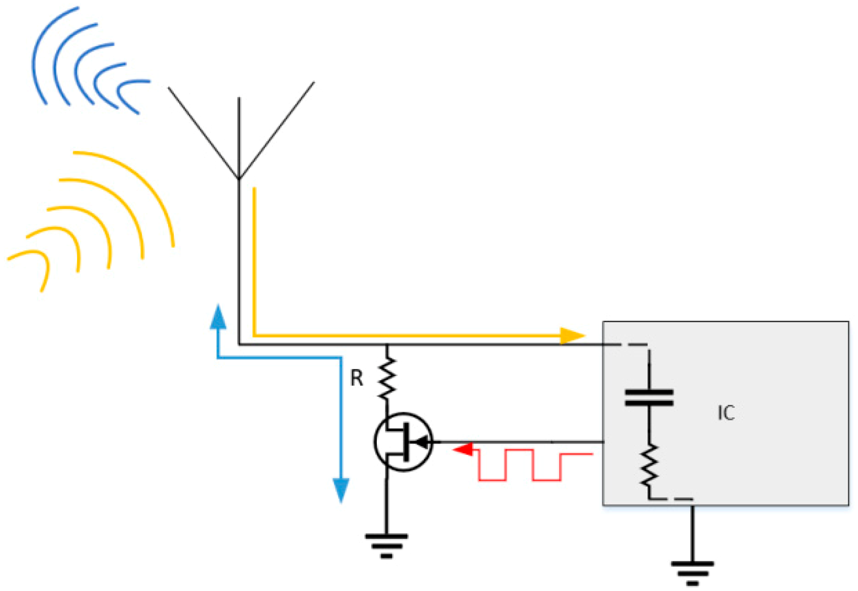
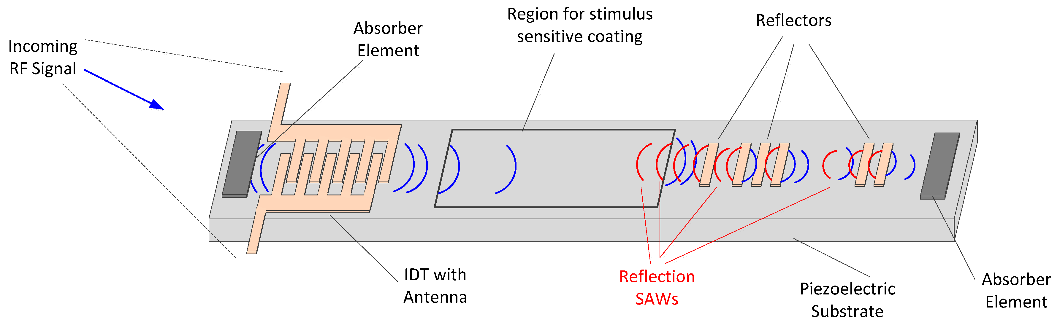
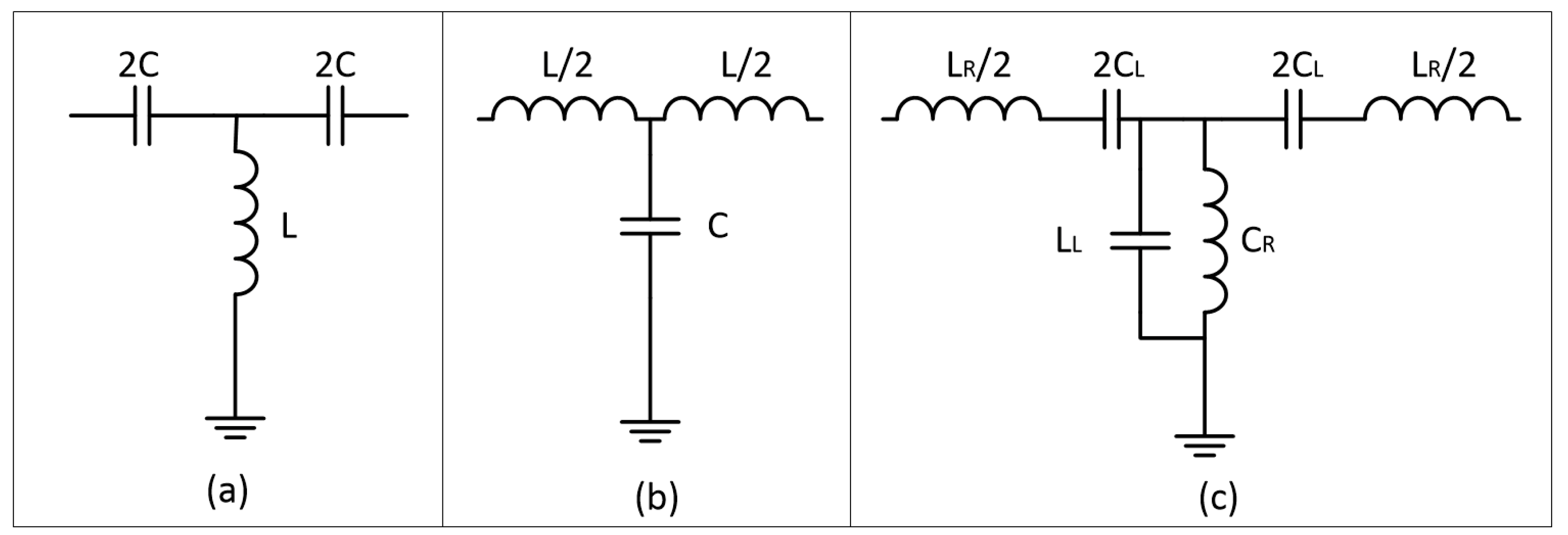

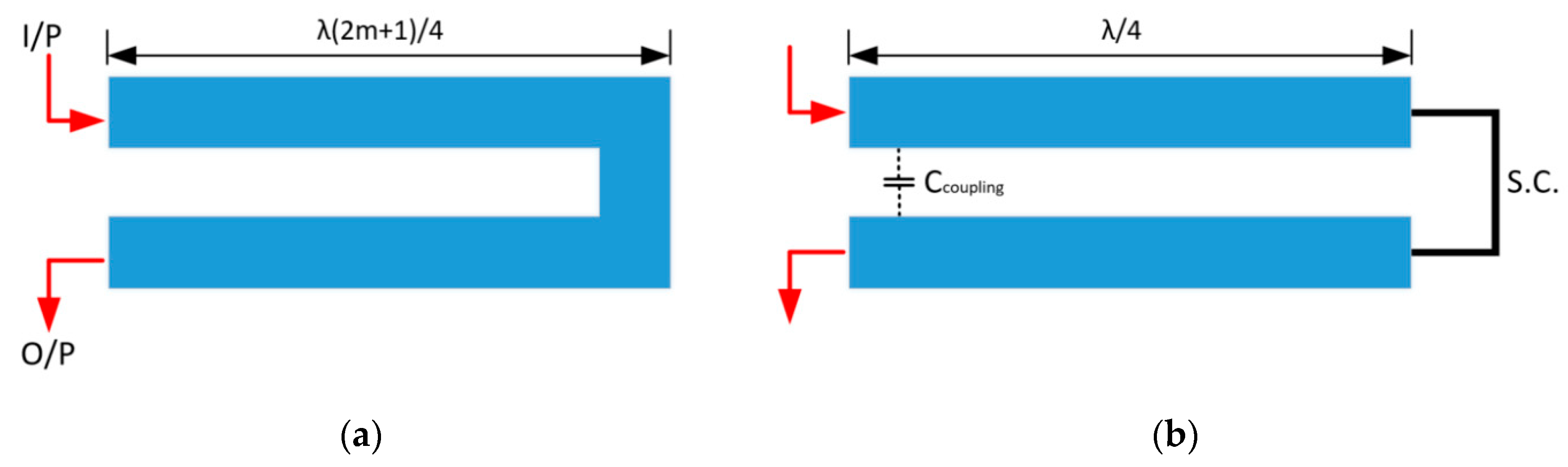


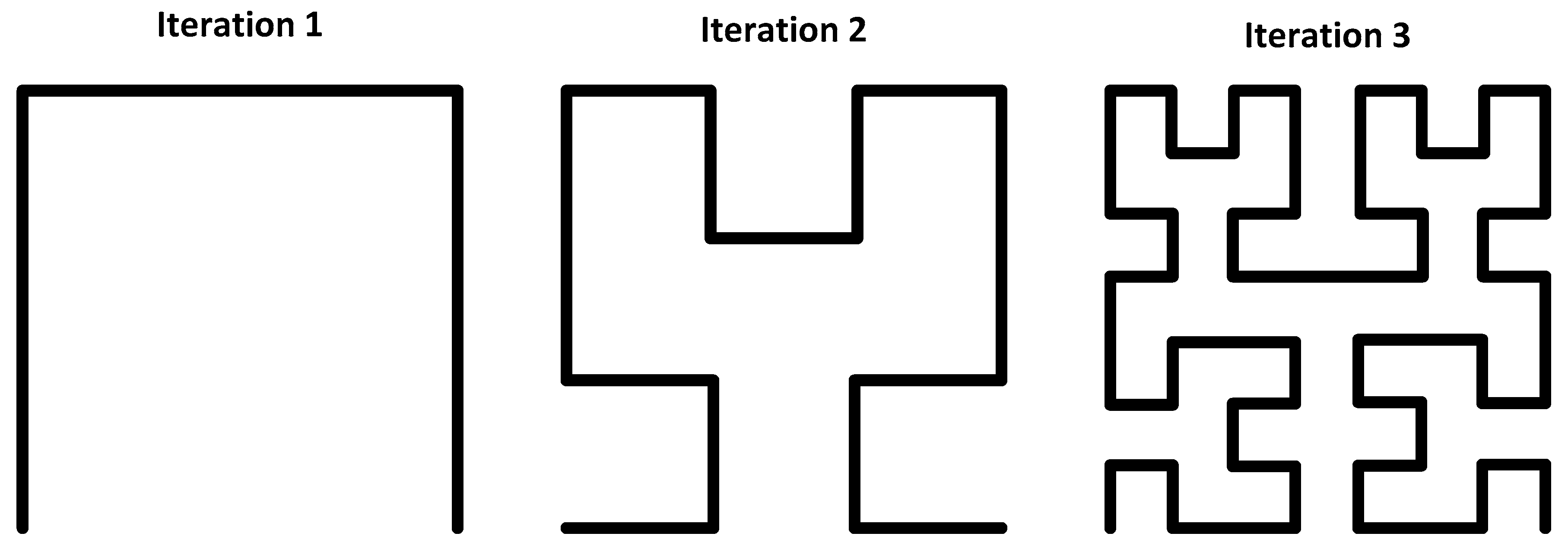
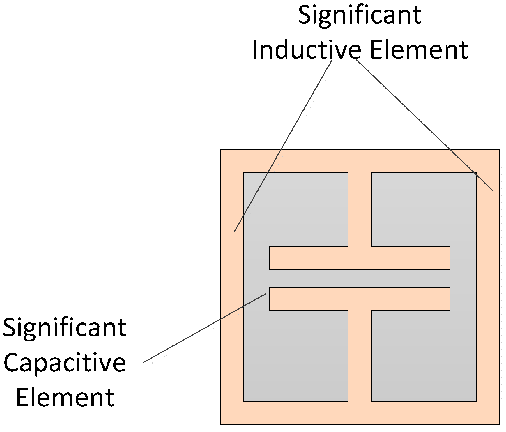
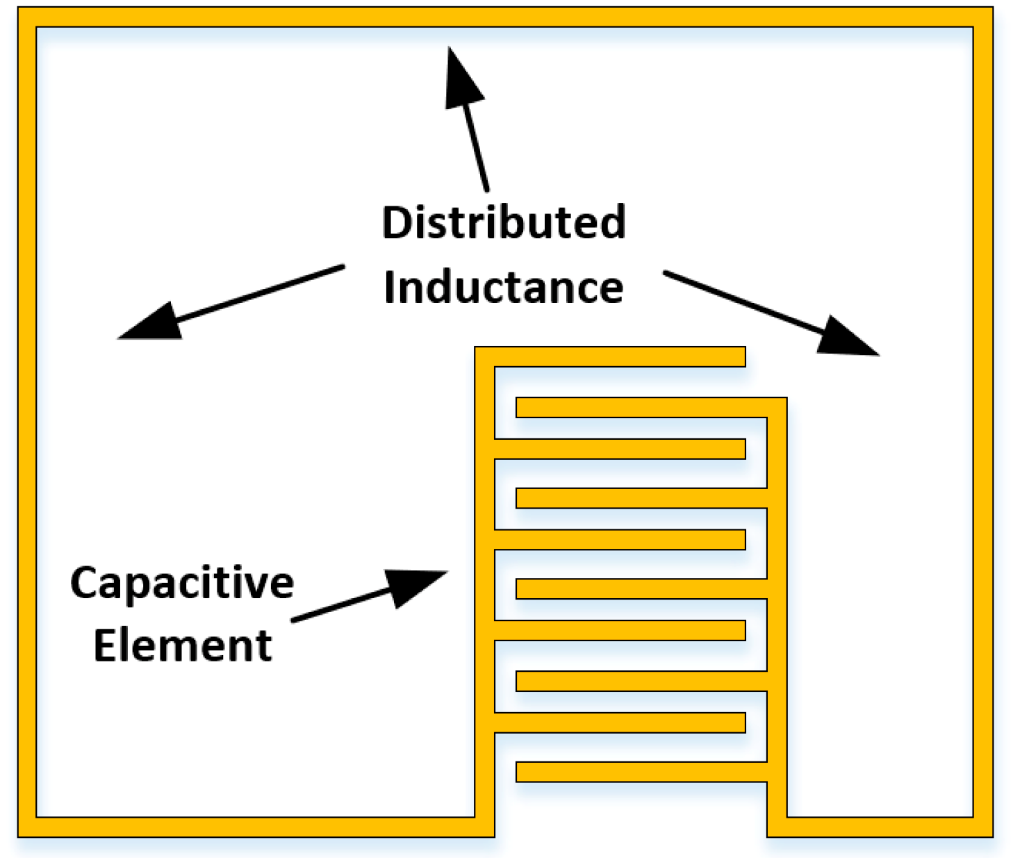
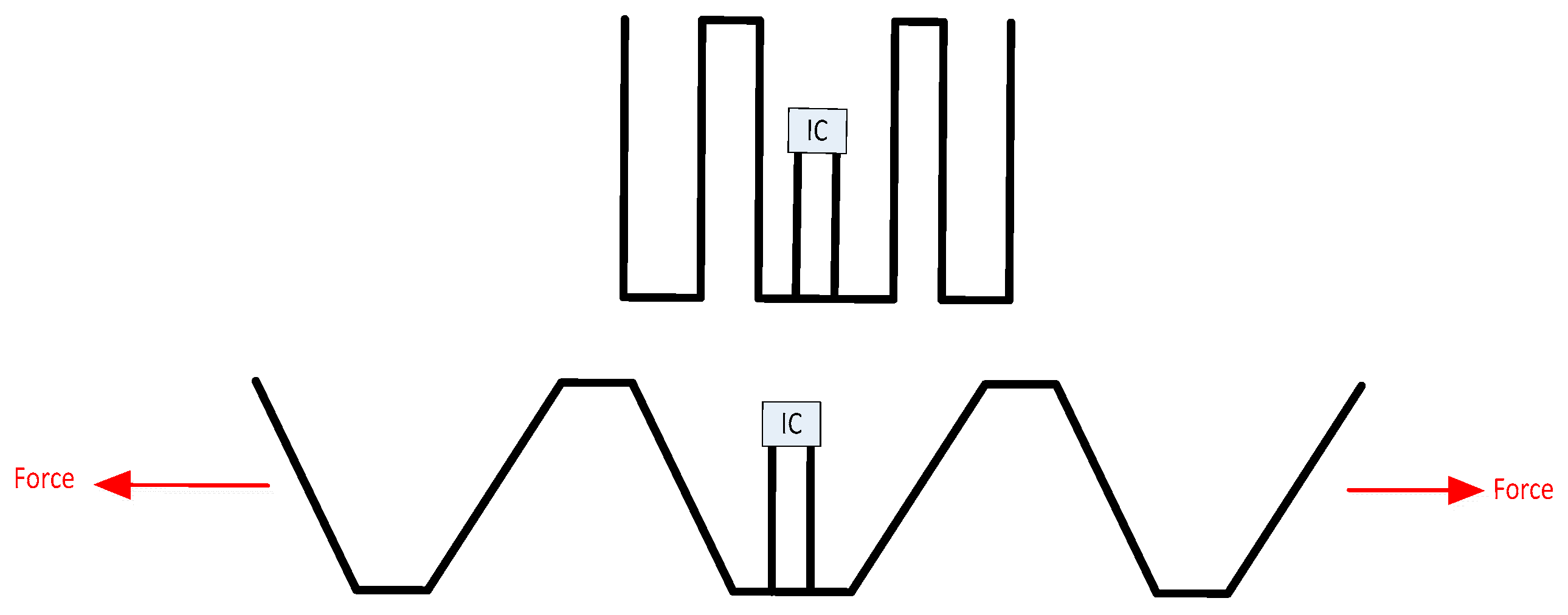
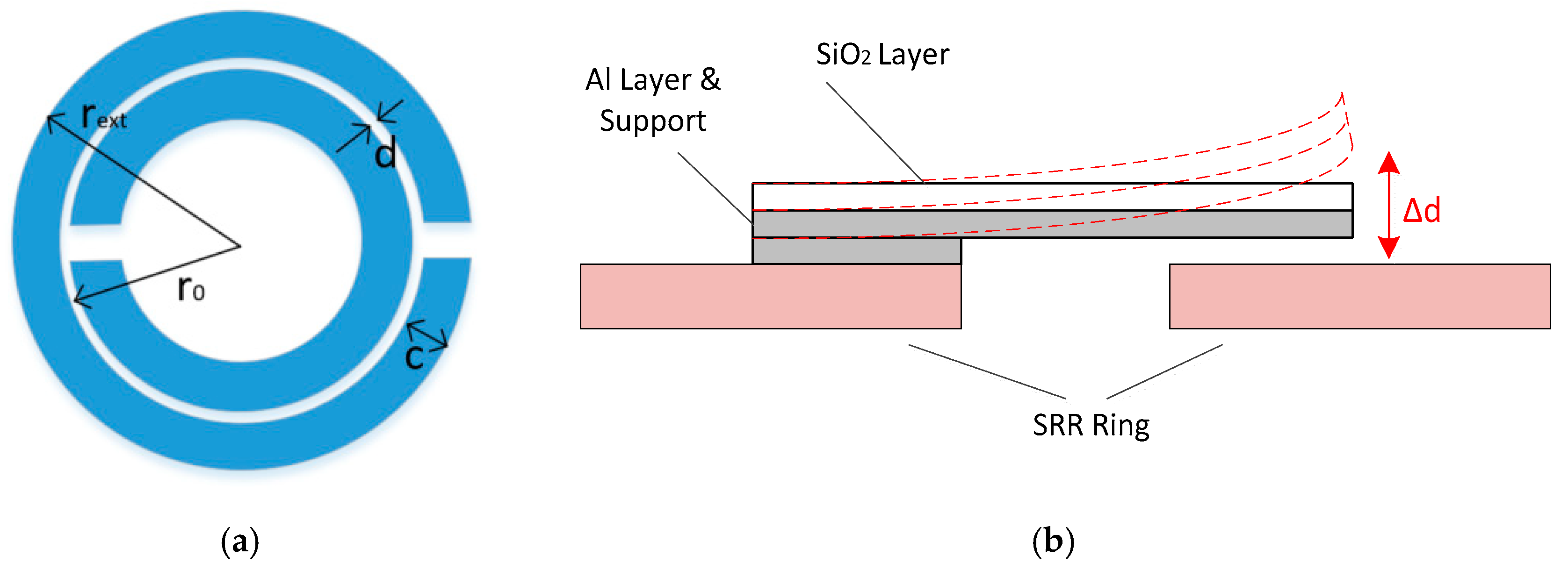

| Tag Design | Year | Major Dimensions | Bits Encoded | Operating Frequency | Interrogation Signal | Reported Read Range | Reader Architecture | Advantages | Disadvantages |
|---|---|---|---|---|---|---|---|---|---|
| SAW | 2002 [66] | n/a | 64 | 2.44 GHz | Sinusoidal pulse | n/a | n/a | High Density | Tight manufacturing tolerances |
| 2004 [67] | n/a | <256 | 2.45 GHz | Sinusoidal pulse | n/a | n/a | High Density | Tight manufacturing tolerances | |
| 2014 [12] | 0.8 × 2.1 mm * | n/a | 2–2.5 GHz | LFM Chirp | n/a | n/a | Very Compact | Requires UWB interrogation | |
| 2004 [68] | 1 cm length * | n/a | 250 ± 50 MHz | Stepped Chirp | n/a | n/a | Robust in multi-sensor environment | Needs accurate reflector design | |
| TFT | 2013 [69] | 3.9 × 1.5 mm * | 16 | n/a | Sinusoid | n/a | 13.56 MHz RFID Reader | Compact | Uses 222 transistors |
| 2006 [61] | n/a | 64 | 13.56 MHz | Sinusoid | n/a | 13.56 MHz RFID Reader | Uses 1938 TFTs | ||
| 2011 [70] | 7 × 10 mm | n/a | 13.56 MHz | Sinusoid | 90 mm | RFID Reader | Works at 13.56 MHz | Uses 1026 TFTs | |
| 2015 [71] | 54 cm2 * | 4 | 13.56 MHz | Sinusoid | 50 mm | RFID Reader | Works at 13.56 MHz | Uses 250 TFTs. Needs large supply voltage | |
| 2017 [57] | 6 × 8.3 mm | 96 | 13.56 MHz | Sinusoid | NFC Design | NFC-Enabled Device | Compact | Unclear if it is capable of >1 m read range | |
| 2018 [72] | 3 × 9 mm * | n/a | Up to 20 MHz | Sinusoid | n/a | RFID Reader | Suitable for Roll-to-Roll fabrication and 20 MHz operation | Not a completed tag | |
| 2013 [62] | 34 mm2 * | 8 | n/a | Sinusoid | n/a | n/a | Compact. Printed with inkjet technology | Not fully integrated into RFID system | |
| Basic Reflection Tag | 2008 [41] | Length > 400 mm * | 8 | 1–3 GHz | Sinusoidal pulse | n/a | TDR Module | Simplistic design | Very sensitive to interference |
| Basic Delay Line | 2006 [40] | 11.2 × 5.3 cm * (***) | 4 | 915 MHz | Sinusoidal pulse | n/a (no wireless element) | RF Generator | Simplistic design | Bit-density is highly driven by pulse duration. Relatively large. Requires isolators |
| 2007 [73] | n/a | 4 | 915 MHz | Sinusoidal pulse | 25.4 cm | VNA (HP4396B) | Simplistic design | Requires isolators, circulators, etc. Scalability and robustness are questionable | |
| UWB Delay Line | 2011 [28] | 57 × 70 mm *** | n/a (3 possible values) | 3.1–10.6 GHz | UWB Impulse | 1.5 m | IR-UWB Radar | No template response needed. Tested at long range | Dual planar, relatively large |
| 2008 [42] | 23 × 31 mm | n/a (3 possible values) | 3.1–10.6 GHz | UWB Impulse | 0.8 m | n/a | Readily supports IR-UWB Radar interrogation | Dual Planar | |
| CRLH Delay Line | 2008 [45] | 120 × 14 × 10 mm * | 4 | Between 2.2 GHz and 4 GHz | Sinusoidal pulse | n/a | n/a | CRLH TL Implemented | Tight tolerances, dispersion issues and high losses occur with CRLH transmission lines |
| 2009 [44] | Length = 26 cm * | 6.2 | 2.2 GHz | Sinusoidal pulse | n/a | Described in Reference [74] | Implements QPSK | ||
| 2017 [49] | Approximate Length = 12 cm * | 2 | 2.4 GHz | Sinusoidal pulse | 14 cm | n/a | More Compact | ||
| Group Delay Tag | 2010 [52] | Width > 37.5 mm * | 3 | 2–4 GHz | Chirp or discrete frequencies | n/a | n/a | Fully printable design | Requires UWB interrogation. Odd Harmonics exist, limiting address space |
| 2013 [75] | 10 × 8 cm (2 × 3 cm without antennas) | 10 ** | n/a | Chirp | 30 cm | VNA (PNA N5222A) | |||
| MIW Tag | 2012 [76] | Height > 20 mm * | 2 | 2.45 GHz | Sinusoidal pulse | n/a | VNA (E8364B) | Fully Printable | Large losses and tight tolerances for Metamaterial Structures and MIW supporting structures |
| 2018 [77] | 28 × 16 mm * | 2 | 2.9 GHz | Sinusoidal pulse | >1 cm | VNA (N9918A FieldFox) |
| Tag Design | Year | Major Dimensions | Bits Encoded | Spectral Use | Starting Frequency | Read Range | Reader | Polarization | Advantages | Disadvantages | ||
|---|---|---|---|---|---|---|---|---|---|---|---|---|
| SIR TL | 2011 [79] | Length > 100 mm * | 2 | 80 MHz | 970 MHz | 27 | 17 | n/a | n/a | Linear | Printable, single-plane design | Sub-mm tolerances. Approximately 50 mm per bit encoded |
| 2016 [84] | 5 × 2.5 cm * | 1024 (Theory) | 5.8 GHz | 180 MHz | 30 | 10 | 2 mm | n/a | n/a | Printable, single-plane design | Requires UWB interrogation | |
| Spiral TL | 2009 [88] | 88 × 65 mm | 35 | 4 GHz | 3 GHz | 12 | 3 | 5–40 cm | VNA (PNAE8361A) | Cross-Polar | Spirals are compact resonators | Designed for 0.4 m read range. Sub-mm tolerances on spirals |
| 2010 [5] | n/a | 6 | 1.6 GHz | 2 GHz | 20 | 5 | 10 cm | n/a | Linear | Single Antenna Design. Spectrally efficient | Tight fabrication tolerances on spirals | |
| Spiral TL Group | 2018 [126] | 14 cm2 | 20 | 1.2 GHz | 2 GHz | 15 | 5 | 25 cm | VNA (R and S ZVA 40) | Largely omni-directional | Compact, single layer design | 66% variation in spectral dips |
| Stub Loaded TL | 2019 [89] | 23.8 × 17 mm * | 10 | 1.84 GHz | 2 GHz | 20 | 3 | n/a | VNA | n/a | Simplistic, compact design | Significant variations in stub insertion loss |
| 2018 [90] | 53 × 34 mm | 12 | 3.25 GHz | 3 GHz | 35 | 22 | n/a | n/a | Cross-Polarized | Compact and smaller variations in stub insertion loss | Uses a significant amount of the spectrum. Only designed for 0.4 m ranges | |
| 2015 [92] | 28 × 20 mm * | 18 | 3 GHz | 3.1 GHz | 15 | 12 | 20 cm | VNA | Cross-Polarized | Very stable stub responses | Uses a significant amount of the spectrum | |
| 2012 [91] | 30 × 25 mm | 8 | 2.2 GHz | 1.9 | 25 | 8 | 40 cm | VNA (PNA E8362B) | Cross-Polarized | Simplistic Design | Only tested at 0.4 m but response was relatively robust | |
| Resonator Based | ||||||||||||
| SIR | 2014 [82] | 42 × 20 mm | 8 | 5.6 GHz including harmonics | 3.4 GHz | 18 | 5 | 20 cm (tests) 40 cm | VNA (PNA E8362B) | Linear | Printable, single-plane design | Uses large amount of spectrum. Only 0.5 m read range recorded |
| 2016 [83] | 55 × 35 mm | 46 | 7.5 GHz | 3.1 GHz | 8 | 3 | 25 cm (tests) 50 cm | VNA (PNA E8362B) | Linear | |||
| Dipole Based | 2014 [99] | 59 × 17 mm | 3 | 3 GHz | 2 GHz | 18 | 7 | 45 cm (tests) 1 m | VNA (PNA E8362B) | Linear | 1 m read range was achieved with 3 dBm Tx power | Relatively large |
| 2018 [100] | 40 × 40 mm | 6 | 4 GHz | 3 GHz | 7 | 3 | 50 cm | VNA | Linear | Simple design with relatively loose tolerances | Not very compact | |
| 2005 [102] | Approximately 50 × 20 mm | 5–11 | 1.1 GHz | 5 GHz | 5 | 2 | n/a | VNA | Linear | Simple design | Not very compact | |
| 2019 [101] | 20 × 20 mm | 8 | 3 GHz | 3 GHz | 20 | 10 | 45 cm | VNA | Omni-directional | Compact. Orientation-independent | Still not as compact as stub loaded TL tags | |
| 2018 [103] | 15 × 15 mm | 6 | 3.5 GHz | 4 GHz | 35 *** | 30 *** | n/a | n/a | ||||
| 2011 [93] | 15 × 15 mm | 16 | 6 GHz | 6 GHz | 10 *** 4 | 2 *** 2 | n/a | VNA (PNA E8361A) | Dual Polarized | Very compact | Poor spectral response | |
| 2016 [127] | 6.8 × 5.5 mm | 3 | 2 GHz | 8.5 GHz | 10 *** | 5 *** | <50 cm | VNA | ||||
| 2017 [105] | 4.5 × 4.5 mm | 4 | 1.4 GHz | 3 GHz | 4 | 2 | 10–20 cm | USRP | Cross-Polar | Very compact | Poor resonant response | |
| Hairpin/C-shaped | 2011 [97] | 40 × 20 mm | 10 | 4 GHz | 2.5 GHz | 18 | 2 | 45 cm | VNA (HP 8720D) | Linear | Encodes in phase and frequency | Not very compact |
| 2016 [96] | 26 × 70 mm | 20 | 2 GHz | 2 GHz | 15 | 4 | 30 cm | VNA (ZVA 40) | Linear | Large bit-density | ||
| 2017 [95] | 40 × 20 mm | 10 | 3 GHz | 2.4 GHz | 25 | 4 | n/a | n/a | Linear | More spectrally efficient than earlier tag | ||
| 2018 [94] | 121 × 10.5 mm | 1 | n/a | 950 MHz | n/a | n/a | n/a | VNA (PNA-X) | Linear | Operates in ISM band | ||
| Slotted Resonator | 2015 [98] | 30 × 30 mm | 12 | 7 GHz | 3 GHz | 4 | 1 | 15 cm | VNA (AV 3629D) | Linear | Relatively compact | Poor spectral use/response |
| 2017 [104] | 24.5 × 25.5 mm | 36 | 13 GHz | 5 GHz | 6 | 2 | n/a | VNA (ZVL13) | Linear | Far more compact | Poor spectral use/response | |
| Ring Resonator | 2012 [106] | 15 × 15 mm | 8 | 6.5 GHz | 6 GHz | 10 | 5 | 20 cm | VNA (PNA E8361A) | Omni-directional | Very compact | Appears to be parasitic coupling between rings |
| 2012 [108] | 30 × 30 mm | 19 | 7.5 GHz | 3.1 GHz | 4 | 2 | 40 cm | VNA (8722D) | Omni-directional | Very compact | Poor spectral response | |
| 2015 [111] | n/a | 8 | 2 GHz | 2.5 GHz | 15 | 5 | 35 cm | USRP2 | Omni-directional | Compact | Apparent low bit-density | |
| 2016 [112] | 20 × 20 mm | 10 | 7 GHz | 4 GHz | 25 *** | 15 *** | n/a | n/a | Omni-directional | Compact | ||
| 2018 [109] | <98 × 98 mm | 13 | 5.5 GHz | 3 GHz | 35 *** | 7.5 *** | n/a | n/a | Omni-directional | Robust RCS response | Significant redundancy in design | |
| Grouped Loop Resonators | 2016 [115] | 20 × 40 mm | 28.5 | 7 GHz | 3 GHz | 15 | 5 | 38 cm | VNA (PNA-LN5232A) | n/a (Bi-directional) | Relatively compact | Only tested up to 30 cm away |
| Grouped LC Resonators | 2011 [120] | 150 × 210 mm | 10 | 110 MHz | 10 MHz | 24 | 22 | 21 cm | VNA | n/a | Address can be modified. Low frequency operation | Not very compact |
| Grouped Rhombic Resonators | 2013 [128] | 70 × 40 mm | 6 | 3 GHz | 3 GHz | 11 | n/a (ASK) | 20 cm | VNA (PNA E8358A) | Linear | Implements ASK—More efficient than OOK | Not very compact |
| Grouped SRRs | 2010 [118] | >18.5 × 8 mm | 4 | 4 GHz | 8 GHz | 35 *** | 25 *** | n/a | n/a | Linear | Simulation and Testbed response appear good | Sub-mm fabrication tolerances (0.0 × mm). Some coupling still exists |
| Space Filling Curves | 2006 [129] 2010 [123] | Approximately 150 × 30 mm | 5 | 1.5 GHz | 3 GHz | 5 | 2 | 1.22 m | VNA (E-5071B) | n/a—supports bi-directional | Good use of spectrum space | Poor measured resonant response |
| SIW Resonator | 2019 [130] | Approximately 25 × 20 mm | n/a | 13 GHz | 22 GHz | 35 | 15 | 10 cm | n/a | n/a orthogonal | Less regulations at these frequencies | Microstrip elements have high losses at these frequencies. More expensive reader required |
| Sensor Stimulus | Year | Tag Type | Major Dimensions | Max Stimulus (Range) | Sensitivity | Comments | Measurement Time |
|---|---|---|---|---|---|---|---|
| Strain | 2014 [172] | Resonant | 30 × 30 mm | 7% | 15–52 MHz/% | Non-linear sensitivity up to 7% but smaller linear regions exist | n/a (Structural or SAW) |
| 2011 [175] | Antenna Impedance | 36 × 36 mm (No strain) | 6% | 0.429 dB/% | Read range dependent on strain. Includes IC | ||
| 2012 [9] | Resonant | 100 × 100 mm (Approximate) | 0.2% | 915 MHz/% | |||
| 2017 [168] | Resonant | 6.3 × 6.3 mm | 21,300 µε | 105.6 MHz/ε | |||
| 2009 [170] | Resonant | 15 mm2 | 6000 µε | 5.148 MHz/ε | |||
| 2015 [10] | SAW/Resonant | 10 × 3 mm * | 130 µε (test limit) | −1.8 ppm/µε | Includes addressing scheme. Highly temperature sensitive | ||
| 2019 [178] | MLA/Resonant | 35 × 15 mm (Approximate) | 50% | 1.2 MHz/% | Tested up to 7.5 m range. Read range dependent on strain. Includes IC | ||
| Crack Detection | 2018 [167] | Resonant/Impedance | 62 × 62 mm | 5 mm | −3.4 MHz/mm | ||
| 2018 [166] | Resonant | n/a (Space Filling Curve) | Single fracture | 4 MHz/crack | |||
| Temperature | 2009 [179] | SAW velocity | n/a | 190 °C | n/a (see Reference [164]) | n/a | |
| 1998 [159] | SAW velocity | n/a | 85 °C | 6.03 kHz/°C | n/a | ||
| 2011 [181] | Transmission Line Termination | n/a | 100 °C | 0.5°/°C | Phase and magnitude encoding | n/a | |
| 2012 [233] | Resonant/Si NWs | 12 × 15 mm (Approximate) | 19 °C | 1.625 MHz/°C (With humidity Change) | 120–255 seconds | ||
| 2018 [180] | Resonant/Substrate-based | 46 × 20 mm (Approximate) | 100 °C | n/a | n/a | ||
| 2015 [139] | Resonant/Graphene Oxide | n/a | 40 °C | −7.69 kHz/°C | n/a | ||
| 2016 [127] | Resonant/Phenanthrene | 6 × 6 mm | 72 °C | Threshold-based—320 MHz change | Single Use | 60 min | |
| 2019 [184] | Resonant and Q factor | 25 × 25 mm | 4, 8, 12, 16 °C Thresholds | Threshold-based | n/a | ||
| 2010 [183] | Resonant/Bi-metallic Strip | 3 × 3 mm * (**) (Approximate) | Up to 300 °C | Up to 780 MHz/°C | Operates between 28 and 34 GHz. Coupled to CPW which has not been included in dimensions | n/a | |
| 2012 [185] | UWB Delay Line/Termination | 10 × 13.65 cm | 25 °C–130 °C | (Approximately) −0.191 dB/°C | Uses SMD termination load. Good read range | 0–3 min | |
| 2015 [186] | UWB Delay Line/Termination | 83.5 × 78.4 mm | n/a | 50 °C Threshold | Uses external thermostat sensor | n/a | |
| Pressure | 2013 [134] | SAW—Resonant | 5 × 5 x 5 mm * | 4 Bar | 0.33 ± 0.02 MHz/Bar | Some hysteretic effects take place. Operates between 10 and 14 GHz | n/a |
| 2006 [163] | SAW—Resonant | Tire valve size (assumed) | 150 Psi | Sub 0.4 Psi resolution | n/a | n/a | |
| 1998 [159] | Saw-Resonant/Velocity | 15 × 15 mm * | 10 Bar | 8.33 kHz/Bar (Estimated) | n/a | n/a | |
| 2013 [164] | OFET/(PMOFET) | 45 × 20 mm ** | 78.125 Mpa | 30.7 mA/Mpa | n/a | n/a | |
| 2009 [169] | Resonant/Diaphragm | 5.8 × 3.8 × 1.4 * | 3 Bar | 370 MHz/Bar | n/a | n/a | |
| Humidity | 2018 [103] | Resonant/PVA | 15 × 15 mm | n/a | n/a | Operates between 4.5 and 7.5 GHz | |
| 2006 [135] | SAW—Resonant and insertion loss/PVA | n/a | 30–90% range | 0.1625 dB/% | Some hysteresis occurs with PVA. Resonant changes were not very linear | n/a | |
| 1.78 kHz/% | |||||||
| 3 kHz/% | |||||||
| 2013 [75] | Group delay and resonant/(Si NWs) | 98 × 63 mm | 60.2–88% range | 0.802 ns/% | All variations were non-linear | ||
| 2016 [127] | Resonant/PVA | 6 × 6 mm | 35–85% | 5.714 MHz/% | n/a | ||
| 2018 [144] | Resonant/Graphene Oxide | 8.5 × 6 mm | 11.3–97.3% | 772.6 kHz/% below 84.3% | Low hysteresis levels | n/a | |
| 3.415 MHz/% above 84.3% | |||||||
| 2015 [139] | Resonant/Graphene Oxide | 10 × 10 mm | 55–95% | 17.8 kHz/% | n/a | ||
| 2018 [100] | Resonant/Si NWs | 40 × 40 mm | 30–90% | 2.9 MHz/% below 70% | 10 min | ||
| 4.8 MHz/% above 70% | |||||||
| 1997 [132] | FET/Polyanailine | Single FET | 15–50% | 0.9615 µA/s/% | Turn on current sensitivity is the variable | n/a | |
| 2017 [145] | (TL) Resonant spiral/PVA | >20 × 10 mm * | 21–53% | 2.5 MHz/% | n/a | ||
| VOC Gasses | 2004 [136] | SAW-Resonant/CNTs | 3 × 1 mm * | Ethanol: 1.3–180 ppm | Ethanol: 6.89 kHz/ppm | Serious recovery issues once stimulus removed | 2–4 min |
| Toulene: 2.8–180 ppm | Toulene: 7.47 kHz/ppm | ||||||
| Ethylacetate: 2.7–180 ppm | Ethylacetate: 5.45 kHz/ppm | ||||||
| 2002 [148] | Resonant/CNTs | 20 × 20 mm | CO2: 20–80% | CO2: %(Δε) = 1/60% | Humidity and temperature variations have unwanted effects. Irreversible NH3 effects | CO2: 45 seconds | |
| O2: 0–100% | O2: %(Δε) = 0.07/100% | ||||||
| O2: 4 min | |||||||
| NH3: 0–100% | NH3: n/a | NH3:2 min | |||||
| 2009 [147] | Resonant-Reflection/CNTs | 118 × 27 mm | n/a | n/a | 10.8 dBi effect of NH3 presence | ||
| 2016 [146] | Resonant/Porous Substrate | 8 × 10 mm * | Acetone: 0.1% | Acetone: 0.875 GHz/% | Desorption time > 15 min | n/a | |
| Methanol: 0.04% | Methanol: 1.5 GHz/% | ||||||
| 2017 [138] | Resonant/Zeolites | >4 × 4 mm * | n/a | <0.5 GHz for various stimuli | Significant purging required after use. Regeneration of zeolites required | 10–20 min | |
| 2013 [137] | Resonant-Impedance/PEUT | n/a | 0–27% RH | 5.926 kHz/% | Allows for temperature compensation | n/a | |
| 2008 [133] | TFT-(Drain-source current)/rr-P3HT | n/a | n/a | %ΔIDS = | 1–2 min | ||
| Acetone: 0.57%/100 ppm | |||||||
| Toluene: 0.2%/280 ppm | |||||||
| Butanol: 0.6%/75 ppm | |||||||
| Orientation/Rotation | 2019 [158] | Polarization | n/a | 360° | Change of 40 dBm in RCS | 0–180 results are equal to 180–360 results. Not linearly sensitive | n/a |
| 2017 [157] | Resonant/Cross-Polar response | 95° | Non-linear magnitude and frequency change | n/a | |||
| Permittivity/Velocity | 2007 [50] | CRLH resonant and phase | n/a | ε = 1.027 led to 180 MHz shift (2500°/ε) | n/a | ||
| 2009 [51] | CRLH Capacitive | n/a | 60° shift experienced for placed item on belt | Phase-based measurement | Measurement issues exist | n/a | |
| 2016 [171] | Resonant-Read Range/substrate permittivity | 39.5 × 25 mm | ε = 2.5–8 | n/a | Non-linear RCS response. Operates at a single frequency | n/a | |
| 2018 [152] | UWB Delay Line | 30 × 30 mm (per cell) | (Non-linear) 20 GHz/% | n/a (Tested up to = 5) | Relies on pre-set polarization | n/a | |
| 2018 [153] | Resonant | >20 × 22 mm (per cell) | −8.474 GHz/% | n/a (Tested up to = 4.54) | Read range enhanced with redundant elements | n/a | |
| 2012 [154] | Resonant Stub | 14 × 14 cm | −2.375 GHz/% | n/a (Tested up to = 4) | Unclear if sensor response is linear | n/a | |
| 2015 [155] | UWB Delay Line—Mode Delay | 58 × 102.5 mm | −16.67 ns/% | n/a (Tested up to = 4.24) | n/a (Negligible) |
© 2019 by the authors. Licensee MDPI, Basel, Switzerland. This article is an open access article distributed under the terms and conditions of the Creative Commons Attribution (CC BY) license (http://creativecommons.org/licenses/by/4.0/).
Share and Cite
Mc Gee, K.; Anandarajah, P.; Collins, D. A Review of Chipless Remote Sensing Solutions Based on RFID Technology. Sensors 2019, 19, 4829. https://doi.org/10.3390/s19224829
Mc Gee K, Anandarajah P, Collins D. A Review of Chipless Remote Sensing Solutions Based on RFID Technology. Sensors. 2019; 19(22):4829. https://doi.org/10.3390/s19224829
Chicago/Turabian StyleMc Gee, Kevin, Prince Anandarajah, and David Collins. 2019. "A Review of Chipless Remote Sensing Solutions Based on RFID Technology" Sensors 19, no. 22: 4829. https://doi.org/10.3390/s19224829