Abstract
A high-performance solar-blind photodetector with a metal–semiconductor–metal structure was fabricated based on amorphous In-doped Ga2O3 thin films prepared at room temperature by radio frequency magnetron sputtering. The photodetector shows a high responsivity (18.06 A/W) at 235 nm with a fast rise time (4.9 μs) and a rapid decay time (230 μs). The detection range was broadened compared with an individual Ga2O3 photodetector because of In doping. In addition, the uneven In distribution at different areas in the film results in different resistances, which causes a quasi-Zener tunneling internal gain mechanism. The quasi-Zener tunneling internal gain mechanism has a positive impact on the fast response speed and high responsivity.
1. Introduction
Ultraviolet light (UV) is electromagnetic radiation, which can be classified into three wavebands: ultraviolet A (UVA, 320–400 nm), ultraviolet B (280–320 nm), and ultraviolet C (UVC, 200–280 nm). UVC light, also known as solar-blind ultraviolet light, is completely absorbed by ozone in the atmosphere and does not exist on the surface of the earth [1,2]. Compared with other light detection technologies, solar-blind ultraviolet light detection technology is less affected by the external environment; the interference of other signal sources on the surface is smaller, and it can work around the clock. Therefore, solar-blind photodetectors based on semiconductor materials with wide-bandgaps, such as AlGaN [3], MgZnO [4], diamond [5,6], and Ga2O3 [7], have received much attention for applications in missile warning, flame sensors, air purification, space communication, and ozone-layer monitoring. Among the materials, MgZnO and AlGaN exhibit serious composition fluctuations or phase segregation. Additionally, the cost of diamond is too high to apply in practical applications [8,9]. As a direct wide-bandgap semiconductor material, Ga2O3 has a bandgap width of ~4.9 eV, which is very suitable for solar-blind UV detection [10,11,12], avoiding the complexities and difficulties of fabricating alloys, such as AlGaN and ZnMgO. In addition, Ga2O3 has great thermal and chemical stability and is inexpensive. Therefore, in recent years, Ga2O3-based deep ultraviolet light detectors have been widely studied.
Ga2O3 consists of five different crystal structures. Monoclinic β-Ga2O3 is the most stable among these structures, and its UV detection properties have drawn increasing attention [13,14]. In 2007, Oshima et al. first reported the metal–-semiconductor–metal (MSM)-type β-Ga2O3 thin film detector prepared on a sapphire substrate by the molecular beam epitaxy (MBE) method [15]. However, high-quality β-Ga2O3 thin film materials demand, for example, a high temperature during fabrication, but high-temperature manufacturing conditions are not suitable for flexible devices [16,17]. In addition, due to the persistent photoconductive effect, the speed of the device response and recovery is greatly reduced even to a level of seconds [18]. Recently, amorphous solar-blind photodetectors have demonstrated fast response speeds and simple processing conditions. In 2017, Shujuan Cui et al. fabricated an amorphous Ga2O3 (a-Ga2O3) photodetector with a responsivity of 0.91 A/W and a fast decay time of 19.1 μs [19]. At the same time, the amorphous film and room temperature promoted the preparation of a flexible device. However, the responsivity needs to be improved, and the response mechanism also needs to be further researched.
Doping is a good method to help change the photoelectric properties of a device. In2O3 is a very important n-type semiconductor with a bandgap of 3.6–3.75 eV and has high conductivity and high transmittance in the visible light region. At the same time, In2O3 also has excellent chemical and thermal stability and is widely used in many fields due to its unique excellent photoelectric properties [20]. In2O3 and Ga2O3 can be properly combined into a new InGaO (IGO) oxide alloy with an adjustable bandgap width between 3.6–4.9 eV, thus the detection range of a photodetector could be broadened.
In this paper, we demonstrated the fabrication of an amorphous In-doped Ga2O3 (a-IGO) thin film MSM photodetector on a sapphire substrate with both high responsivity and fast response speed. We found that In doping leads to the bandgap change, which is the reason for the larger detection range. The photoelectrical characteristics and mechanisms of the fabricated devices were also investigated.
2. Materials and Methods
The a-IGO thin films were grown on c-plane sapphire substrates by radio frequency (RF) magnetron sputtering, and the sputtering target was an IGO ceramic target (Ga:In = 5:2 at%). The sapphire substrates were cleaned in acetone, ethanol and deionized water for 45 min using an ultrasonic cleaning machine. The chamber base pressure was maintained at 5 × 10⁻⁴ Pa. The sputtering process was carried out for 35 min with a working pressure of 5 Pa, a sputtering power of 80 W, and an Ar flow rate of 40 sccm. The film thickness was approximately 200 nm. To fabricate the MSM detectors, a 50 nm Au film was deposited on the a-IGO film by thermal evaporation. Then, the Au film was lithographed with a mask. As shown in Figure 1a,b, the length of the fabricated detector electrodes was 500 μm, and the finger spacing and width were 5 and 10 μm, respectively.
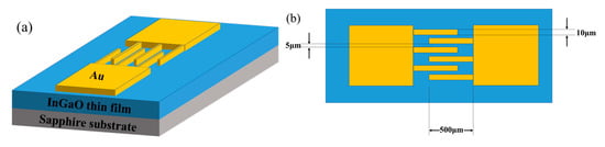
Figure 1.
(a) The device diagram and (b) the finger diagram of the a-IGO thin film solar-blind photodetector.
The thickness was estimated by a surface profile scanner using the steps between film and the substrate. The structure and orientation of the film were tested by D/max-RA X-ray diffraction (XRD and GI-XRD, RIGAKU SmartLab). The film surface roughness and resistance distribution were determined by atomic force microscopy (AFM, Bruker Dimension ICON) and conductive atomic force microscopy (CFM) measurements. The In content and distribution of the films were characterized by energy-dispersive X-ray spectroscopy (EDX, HITACHI SU-70). The transmission rate was tested using a Shimadzu UV-2450PC scanning spectrophotometer, and the detection range and bandgap were also calculated. The important responsivity and response speed parameters are shown from Zolix Solar Cell Scan 100 measurement system (200 W UV-enhanced Xe lamp with a monochromator and Keithley 2450) and transient response test system.
3. Results and Discussion
Figure 2a shows the normal XRD spectra of the IGO thin film. From the normal XRD results, there are only two diffraction peaks, namely, (0003) and (0006), that belong to sapphire. To prove that the IGO thin film is amorphous, the characterization of the XRD grazing incidence is necessary. Figure 2b shows the grazing incidence XRD results of the IGO thin film. No obvious peak could be found, which indicates that the film is amorphous. We can obtain the film surface information from AFM. Figure 3 is the AFM image with a 5 μm × 5 μm scanning area. The a-IGO film is very smooth and exhibits a small roughness of ~1 nm, which is consistent with the amorphous characteristic of the film.
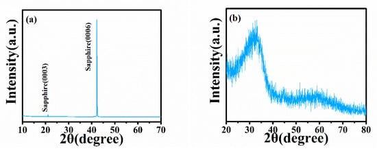
Figure 2.
(a) Normal XRD spectra and (b) XRD grazing incidence (X-ray angle 0.8°) spectra of the a-InGaO thin film.
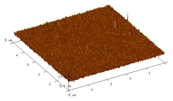
Figure 3.
AFM image of the a-IGO thin film surface.
EDX analysis was performed to evaluate the In, Ga, and O contents and distributions in the a-IGO thin film, as shown in Figure 4, with highlight points. In was successfully doped in Ga2O3; the In element content was 3.48%, the Ga element content was 10.94%, and the O content was ~85.58%. From Figure 4a,b, the distributions of Ga and O elements are even. There are some obvious dark areas where there are no In elements, as shown in Figure 4c. Figure 4d depicts the scanning results of four small areas, and the results indicate that the contents of the different areas are clearly different, which indicates that the In distribution is uneven.
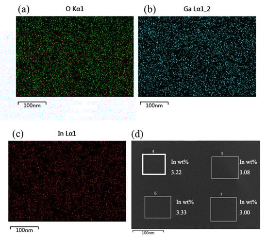
Figure 4.
Elemental maps via EDX: (a) O; (b) Ga; and (c) In. (d) Small area scanning of the four different areas.
Figure 5a is the transmission spectrum of the a-IGO thin film, and the average transmittance in the visible light range is near 85%. For UV light, the transmittance decreases rapidly below 280 nm, and it is close to zero at 200 nm, which indicates that the rate is very low in the range of UVC light. The absorption coefficient can be given by the relation T = Aexp(−αd); d is the film thickness, A is a constant, T is the transmittance [21], and the result is shown in Figure 5b. As the wavelength increases, the absorption rate decreases rapidly. The absorption rate decreases to near zero at approximately 320 nm, which is the absorption cutoff edge of this film. The bandgap Eg can be estimated by the equation (αhv)2 = B(hv − Eg); B is a constant, hv is the photo energy [22]. As shown in the inset of Figure 5b, Eg can be extracted from a linear extrapolation of (αhv)2; the photon energy at the point where (αhv)2 = 0 is Eg. The obtained Eg is ~4.2eV; it decreases compared to ~4.9eV of Ga2O3, which is consistent with references [23,24,25].
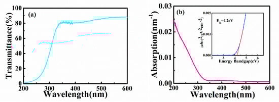
Figure 5.
(a) The transmission spectrum of the a-IGO thin film. (b) The absorption spectrum of the film; the inset shows the plot of (αhv)2 versus energy bandgap.
Above the a-IGO thin film, we fabricated Au finger electrodes by lithography to be a photodetector. Figure 6a shows the responsivity under different voltage conditions. The responsivity increases with increasing voltage. The highest responsivity reaches 18.06 A/W under 25 V at 235 nm, which is between the solar-blind wave range. The photodetector also has a larger detection range, which reveals the changeable bandgap because of In doping and proves that the bandgap of Ga2O3 decreased. The test range is broadened to 210–330 nm, which is wider than the individual Ga2O3 photodetector.
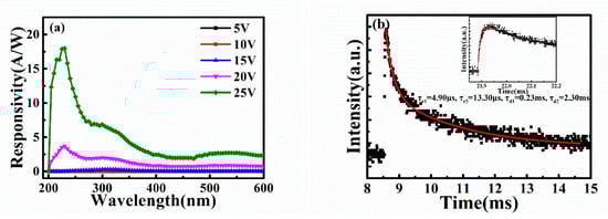
Figure 6.
(a) The responsivity spectra and (b) the time-dependent photoresponse curve of the a-IGO photodetector under 255 nm illumination.
As a photodetector, the response speed is a key parameter. Figure 6b exhibits the response time curves of the detector. When the detector was illuminated by the 255 nm light, the photocurrent increased rapidly. After the light was turned off, the detector needs time, which is decay time (longer than the rise time), to recover to the dark current. To obtain the specific numbers of the rise time and decay time, the response curves were fitted, and these constants were analyzed by the double exponential equation:
In this equation, y0 is the steady-state dark current, y1 and y2 are both constants, t refers to the time, and and stand for the relaxation time, including the fast and slow two stages of the rise time () and decay time (). From the well-fitted curves, the rise time (τr1/τr2 = 4.9 μs/13.3 μs) and decay time (τd1/τd2 = 0.23 ms/2.3 ms) results are faster than those of the other Ga2O3-based solar-blind photodetectors listed in Table 1.

Table 1.
Comparison of key parameters of the different solar-blind photodetectors.
As previously mentioned, the speed of the device response and recovery are greatly reduced because of the persistent photoconductive effect of the β-Ga2O3 thin film detector [19]. However, our photodetector both has fast response speed and high responsivity. Therefore, the a-IGO photodetector may have a different response mechanism than the crystallization photodetector. The current–voltage (I–V) characteristic is shown in Figure 7a with dark current and photocurrents, which were measured at 235 nm. As shown in the Figure 7a, the dark current below ~13 V is small and increases significantly above ~13 V. There is an obvious kink point at ~13 V, which implies that the device has a breakdown voltage of ~13 V at room temperature. There may be two recoverable breakdown internal gains, an avalanche gain mechanism or a Zener tunneling effect. To determine what the internal gain type is, we tested the dark current at changeable temperatures (I–V curves at different temperatures are shown in Figure 7b and the inset figure). The tunnel breakdown voltage decreases from 13 V under 300 K, which is close to room temperature to 6.5 V under 400 K. Through a calculation, the temperature coefficient is negative, −0.065 V/K, which indicates that the gain in our a-IGO photodetector could be a quasi-Zener tunneling effect.
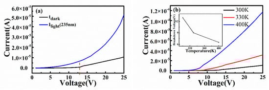
Figure 7.
(a) The dark and light I–V curves of a-IGO photodetector and (b) variable temperature I–V curves without light; the inset shows the relationship between breakdown voltage and temperature.
The breakdown phenomenon always occurs in some types devices, such as the avalanche photodetector (APD), metal–insulator–semiconductor (MIS) tunnel junction, and the p–n junction [31,32,33]. The quasi-Zener tunneling effect that exists in our detector indicates that there may be different resistance areas between which barriers exist. CFM tests were carried out to determine the surface dark current density. As shown in Figure 8, the resistance distribution in the a-IGO thin film is not uniform, and the resistance values of different regions are different. This phenomenon may be due to the uneven distribution of In, which can be seen in Figure 4c. There are some obvious dark areas in the In distribution mapping. Figure 4d, which is the small area scanning of EDX, shows that the In contents are different at different areas in the film. The low resistance regions have high In content, and the high resistance regions have low In content [34]. The thin high resistance regions are shown in Figure 8.
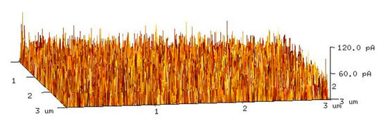
Figure 8.
The CFM result of the dark current distribution under a 5 V bias voltage.
When a small bias voltage is applied to both ends of the electrode, most of the carriers cannot jump over the barrier formed by the high resistance region. Carriers are blocked by a distributed small area of high resistance, and Idark of the a-IGO detector is relatively smaller. As the bias voltage increases to the breakdown voltage, a large number of carriers in the low resistance region can break through the high resistance region by tunneling which usually occurs in MIS-structure tunnel junction detectors [33], and an internal gain mechanism appears. The formula for the carrier tunneling probability is:
Here, , and are constants, represents the barrier of the high resistance region, and d represents the distance of tunneling. The distance d can be seen as the effective thickness, and the probability of tunneling Tt increases exponentially with and d decreasing. When the device is exposed to deep ultraviolet light, the photogenerated carriers appeared in both high resistance areas and low resistance areas. The photogenerated carriers drop the effective thickness and barrier of the high resistance regions, and also increase the carrier concentration of the low resistance regions. Therefore, the carrier tunneling probability increases, and the photocurrent increases exponentially and is much higher than the dark current. The switching between the above block process and tunneling process is very quick, which has been reported in MIS-structure tunnel junction detectors [35]. So our a-IGO photodetector with quasi-Zener tunneling effect exhibits faster response and recovery speed compared to other crystallization devices with persistent photoconductive effect.
4. Conclusions
In summary, the In-doped Ga2O3 amorphous thin film was successfully deposited on sapphire by RF sputtering at room temperature. A fast response MSM solar-blind photodetector with a higher responsibility of 18.06 A/W under a 25 V bias voltage was fabricated based on the film. The rise time and decay time reached 4.9 and 230 μs, respectively. The uneven In distribution results in the quasi-Zener tunneling effect improved the photodetector’s key parameters. Simultaneously, In doping changed the bandgap of the films, and thus, the detection range of the photodetector was broadened from 210 to 330 nm. The high-performance a-IGO solar-blind photodetector preparation at room temperature is very important for flexible devices; additionally, the process is inexpensive and can be developed in for applications in different fields.
Author Contributions
Writing—original draft preparation, M.F. (Mingzhi Fang); Some experiments, M.F. (Mingzhi Fang), W.Z. and F.L.; Writing—review and editing, D.Z., S.H.; Conceptualization, D.Z., S.H. and W.X.; Methodology and data curation, M.F. (Mingzhi Fang), W.L. and P.C.; Formal analysis and validation, M.F. (Ming Fang) and Y.L.; Funding acquisition, D.Z. All authors have read and agreed to the published version of the manuscript.
Funding
This work is supported by the National Natural Science Foundation of China (Grant Nos. 61704111, 51872187, 11774241, 21805194 and 51371120), the Natural Science Foundation of Guangdong Province (Grant No. 2017A030310524), and the Science and Technology Foundation of Shenzhen (Grant Nos. JCYJ20170818143417082, JCYJ20170817100611468 and JCYJ20180508163404043).
Conflicts of Interest
The authors declare no conflict of interest.
References
- Su, L.; Yang, W.; Cai, J.; Chen, H.; Fang, X. Self-Powered Ultraviolet Photodetectors Driven by Built-In Electric Field. Small 2017, 13, 1701687. [Google Scholar] [CrossRef] [PubMed]
- Zhuo, R.; Wu, D.; Wang, Y.; Wu, E.; Jia, C.; Shi, Z.; Xu, T.; Tian, Y.; Li, X. A self-powered solar-blind photodetector based on a MoS2/β-Ga2O3 heterojunction. J. Mater. Chem. C 2018, 6, 10982–10986. [Google Scholar] [CrossRef]
- Kang, S.; Nandi, R.; Kim, H.; Jeong, K.-U.; Lee, C.-R. Synthesis of n-AlGaN nanoflowers by MOCVD for high-performance ultraviolet-C photodetectors. J. Mater. Chem. C 2018, 6, 1176–1186. [Google Scholar] [CrossRef]
- Yang, J.-L.; Liu, K.-W.; Shen, D.-Z. Recent progress of ZnMgO ultraviolet photodetector. Chin. Phys. B 2017, 26, 47308. [Google Scholar] [CrossRef]
- Chen, Y.-C.; Lu, Y.-J.; Lin, C.-N.; Tian, Y.-Z.; Dong, L.; Shan, C.-X.; Gao, C. Self-powered diamond/β-Ga2O3 photodetectors for solar-blind imaging. J. Mater. Chem. C 2018, 6, 5727–5732. [Google Scholar] [CrossRef]
- Balducci, A.; Milani, E.; Morgada, M.E.; Tucciarone, A.; Rinati, G.V.; Angelone, M.; Marinelli, M.; Pillon, M. Extreme ultraviolet single-crystal diamond detectors by chemical vapor deposition. Appl. Phys. Lett. 2005, 86, 193509. [Google Scholar] [CrossRef]
- Pearton, S.J.; Yang, J.; Cary, P.H.; Ren, F.; Kim, J.; Tadjer, M.J.; Mastro, M.A. A review of Ga2O3 materials, processing, and devices. Appl. Phys. Rev. 2018, 5, 011301. [Google Scholar] [CrossRef]
- Ai, M.; Guo, D.; Qu, Y.; Cui, W.; Wu, Z.; Li, P.; Li, L.; Tang, W. Fast-response solar-blind ultraviolet photodetector with a graphene/β-Ga2O3/graphene hybrid structure. J. Alloys Compd. 2017, 692, 634–638. [Google Scholar] [CrossRef]
- Auer, E.; Liao, M.; Koide, Y.; Li, L.; Fang, X.; Zhai, T.; Gautam, U.K.; Lugstein, A.; Bando, Y.; Golberg, D. Deep-ultraviolet solar-blind photoconductivity of individual gallium oxide nanobelts. Nanoscale 2011, 3, 1120. [Google Scholar]
- Qin, Y.; Long, S.; Dong, H.; He, Q.; Jian, G.; Zhang, Y.; Hou, X.; Tan, P.; Zhang, Z.; Lv, H.; et al. Review of deep ultraviolet photodetector based on gallium oxide. Chin. Phys. B 2019, 28, 018501. [Google Scholar] [CrossRef]
- Mastro, M.A.; Kuramata, A.; Calkins, J.; Kim, J.; Ren, F.; Pearton, S.J. Perspective—Opportunities and Future Directions for Ga2O3. ECS J. Solid State Sci. Technol. 2017, 6, P356–P359. [Google Scholar] [CrossRef]
- Khodaparast, G.A.; Xu, Y.V.; Wu, J.; Dravid, V.P.; Pavlidis, D.; Razeghi, M.; McClintock, R.; Park, J.-H.; Magill, B.A. A review of the growth, doping, and applications of Beta-Ga2O3 thin films. Oxide-Based Mater. Devices IX 2018, 10533, 105330R. [Google Scholar]
- Galazka, Z. β-Ga2O3 for wide-bandgap electronics and optoelectronics. Semicond. Sci. Technol. 2018, 33, 113001. [Google Scholar] [CrossRef]
- Dong, L.; Jia, R.; Xin, B.; Peng, B.; Zhang, Y. Effects of oxygen vacancies on the structural and optical properties of beta-Ga2O3. Sci. Rep. 2017, 7, 40160. [Google Scholar] [CrossRef]
- Oshima, T.; Okuno, T.; Fujita, S. Ga2O3 Thin Film Growth onc-Plane Sapphire Substrates by Molecular Beam Epitaxy for Deep-Ultraviolet Photodetectors. Jpn. J. Appl. Phys. 2007, 46, 7217–7220. [Google Scholar] [CrossRef]
- Lee, S.H.; Bin Kim, S.; Moon, Y.-J.; Kim, S.M.; Jung, H.J.; Seo, M.S.; Lee, K.M.; Kim, S.-K.; Lee, S.W. High-Responsivity Deep-Ultraviolet-Selective Photodetectors Using Ultrathin Gallium Oxide Films. ACS Photon. 2017, 4, 2937–2943. [Google Scholar] [CrossRef]
- Nagarajan, L.; De Souza, R.A.; Samuelis, D.; Valov, I.; Börger, A.; Janek, J.; Becker, K.-D.; Schmidt, P.C.; Martin, M. A chemically driven insulator–metal transition in non-stoichiometric and amorphous gallium oxide. Nat. Mater. 2008, 7, 391–398. [Google Scholar] [CrossRef]
- Qian, L.-X.; Wu, Z.-H.; Zhang, Y.-Y.; Lai, P.T.; Liu, X.-Z.; Li, Y.-R. Ultrahigh-Responsivity, Rapid-Recovery, Solar-Blind Photodetector Based on Highly Nonstoichiometric Amorphous Gallium Oxide. ACS Photon. 2017, 4, 2203–2211. [Google Scholar] [CrossRef]
- Cui, S.; Mei, Z.; Zhang, Y.; Liang, H.; Du, X. Room-Temperature Fabricated Amorphous Ga2O3 High-Response-Speed Solar-Blind Photodetector on Rigid and Flexible Substrates. Adv. Opt. Mater. 2017, 5, 1700454. [Google Scholar] [CrossRef]
- Chen, S.; Long, Y.-Z.; Zhang, H.-D.; Liu, S.-L.; Liu, L.-Z.; Zhang, J.-C.; Liu, G.-X.; Shan, F.-K. Fabrication of ultrathin In2O3 hollow fibers for UV light sensing. Phys. Scr. 2014, 89, 115808. [Google Scholar] [CrossRef]
- Zhu, D.L.; Xiang, H.F.; Cao, P.J.; Jia, F.; Liu, W.J.; Han, S.; Ma, X.C.; Lu, Y.M. Influence of H2 introduction on properties in Al-doped ZnO thin films prepared by RF magnetron sputtering at room temperature. J. Mater. Sci. 2013, 24, 1966–1969. [Google Scholar] [CrossRef]
- Zhao, L.; Shao, G.-J.; Qin, X.-J.; Han, S.-H.-Z. Concentration-dependent behavior of hydrogen in Al-doped ZnO thin films. J. Alloys Compd. 2011, 509, L297–L300. [Google Scholar] [CrossRef]
- Tian, W.; Zhi, C.; Zhai, T.; Chen, S.; Wang, X.; Liao, M.; Golberg, D.; Bando, Y. In-doped Ga2O3 nanobelt based photodetector with high sensitivity and wide-range photoresponse. J. Mater. Chem. 2012, 22, 17984. [Google Scholar] [CrossRef]
- Chang, S.-P.; Chang, L.-Y.; Li, J.-Y. The Influence of Different Partial Pressure on the Fabrication of InGaO Ultraviolet Photodetectors. Sensors 2016, 16, 2145. [Google Scholar] [CrossRef]
- Chang, T.-H.; Chang, S.-J.; Weng, W.-Y.; Chiu, C.-J.; Wei, C.-Y. Amorphous Indium–Gallium–Oxide UV Photodetectors. IEEE Photon. Technol. Lett. 2015, 27, 2083–2086. [Google Scholar] [CrossRef]
- Liu, X.; Guo, P.; Sheng, T.; Qian, L.; Zhang, W.; Li, Y. β-Ga2O3 thin films on sapphire pre-seeded by homo-self-templated buffer layer for solar-blind UV photodetector. Opt. Mater. 2016, 51, 203–207. [Google Scholar] [CrossRef]
- Arora, K.; Goel, N.; Kumar, M.; Kumar, M. Ultrahigh Performance of Self-Powered β-Ga2O3 Thin Film Solar-Blind Photodetector Grown on Cost-Effective Si Substrate Using High-Temperature Seed Layer. ACS Photon. 2018, 5, 2391–2401. [Google Scholar] [CrossRef]
- Pratiyush, A.S.; Krishnamoorthy, S.; Solanke, S.V.; Xia, Z.; Muralidharan, R.; Rajan, S.; Nath, D.N. High responsivity in molecular beam epitaxy grown β- Ga2O3 metal semiconductor metal solar blind deep-UV photodetector. Appl. Phys. Lett. 2017, 110, 221107. [Google Scholar] [CrossRef]
- Alema, F.; Hertog, B.; Ledyaev, O.; Volovik, D.; Thoma, G.; Miller, R.; Osinsky, A.; Mukhopadhyay, P.; Bakhshi, S.; Ali, H.; et al. Solar blind photodetector based on epitaxial zinc doped Ga2O3 thin film. Physica Status Solidi (A) 2017, 214, 1600688. [Google Scholar] [CrossRef]
- Oh, S.; Jung, Y.; Mastro, M.A.; Hite, J.K.; Eddy, C.R., Jr.; Kim, J. Development of solar-blind photodetectors based on Si-implanted beta- Ga2O3. Opt. Express 2015, 23, 28300–28305. [Google Scholar] [CrossRef]
- Zhao, B.; Wang, F.; Chen, H.; Wang, Y.; Jiang, M.; Fang, X.; Zhao, D. Solar-Blind Avalanche Photodetector Based On Single ZnO–Ga2O3Core–Shell Microwire. Nano Lett. 2015, 15, 3988–3993. [Google Scholar] [CrossRef] [PubMed]
- Davids, P.S.; Jarecki, R.L.; Starbuck, A.; Burckel, D.B.; Kadlec, E.A.; Ribaudo, T.; Shaner, E.A.; Peters, D.W. Infrared rectification in a nanoantenna-coupled metal-oxide-semiconductor tunnel diode. Nat. Nanotechnol. 2015, 10, 1033–1038. [Google Scholar] [CrossRef] [PubMed]
- Jeong, I.-S.; Kim, J.H.; Im, S. Ultraviolet-enhanced photodiode employing n-ZnO/p-Si structure. Appl. Phys. Lett. 2003, 83, 2946–2948. [Google Scholar] [CrossRef]
- Von Wenckstern, H.; Splith, D.; Purfürst, M.; Zhang, Z.; Kranert, C.; Muller, S.; Lorenz, M.; Grundmann, M. Structural and optical properties of (In,Ga)2O3 thin films and characteristics of Schottky contacts thereon. Semicond. Sci. Technol. 2015, 30, 024005. [Google Scholar] [CrossRef]
- Green, M.; King, F.; Shewchun, J. Minority carrier MIS tunnel diodes and their application to electron- and photo-voltaic energy conversion—I. Theory. Solid-State Electron. 1974, 17, 551–561. [Google Scholar] [CrossRef]


© 2019 by the authors. Licensee MDPI, Basel, Switzerland. This article is an open access article distributed under the terms and conditions of the Creative Commons Attribution (CC BY) license (http://creativecommons.org/licenses/by/4.0/).