Cantilever Type Acceleration Sensors Made by Roll-to-Roll Slot-Die Coating


Abstract
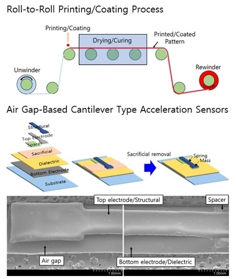
1. Introduction
2. Materials and Methods
3. Results and Discussion
3.1. Air Gap and Dimension of the Sensor Samples
3.2. Electrical Characteristics of the Sensor Samples
4. Conclusions
Author Contributions
Funding
Conflicts of Interest
References
- Al-Sarawi, S.F.; Mukhiya, R.; Varadan, V.K.; Gangopadhyay, S.; Guha, B.; Weste, N.; Kalantar-Zadeh, K.; Bhattacharyya, T.K.; Boni, A.; Zen, M.; et al. MEMS accelerometer-driven fuel-control system for automobile applications. Proc. SPIE 2008, 7268, 72680. [Google Scholar]
- Ciuti, G.; Ricotti, L.; Menciassi, A.; Dario, P. MEMS sensor technologies for human centred applications in healthcare, physical activities, safety and environmental sensing: A review on research activities in Italy. Sensors 2015, 15, 6441–6468. [Google Scholar] [CrossRef] [PubMed]
- Leu, F.Y.; Ko, C.Y.; Lin, Y.C.; Susanto, H.; Yu, H.C. Fall Detection and Motion Classification by Using Decision Tree on Mobile Phone. In Smart Sensors Networks; Academic Press: Cambridge, MA, USA, 2017; pp. 205–237. [Google Scholar]
- Niu, W.; Fang, L.; Xu, L.; Li, X.; Huo, R.; Guo, D.; Qi, Z. Summary of Research Status and Application of MEMS Accelerometers. J. Comput. Commun. 2018, 6, 215–221. [Google Scholar] [CrossRef]
- Park, D.H.; Shin, S.; Kim, Y.K. Module packaging effects on MEMS airbag sensor performance for automobiles. Microelectron. Reliab. 2017, 79, 328–335. [Google Scholar] [CrossRef]
- He, J.; Xie, J.; He, X.; Du, L.; Zhou, W. Analytical study and compensation for temperature drifts of a bulk silicon MEMS capacitive accelerometer. Sens. Actuators A Phys. 2016, 239, 174–184. [Google Scholar] [CrossRef]
- Mukhiya, R.; Garg, M.; Gaikwad, P.; Sinha, S.; Singh, A.K.; Gopal, R. Electrical equivalent modeling of MEMS differential capacitive accelerometer. Microelectron. J. 2020, 99, 104770. [Google Scholar] [CrossRef]
- Shen, Z.; Tan, C.Y.; Yao, K.; Zhang, L.; Chen, Y.F. A miniaturized wireless accelerometer with micromachined piezoelectric sensing element. Sens. Actuators A Phys. 2016, 241, 113–119. [Google Scholar] [CrossRef]
- Tian, B.; Liu, H.; Yang, N.; Zhao, Y.; Jiang, Z. Design of a Piezoelectric Accelerometer with High Sensitivity and Low Transverse Effect. Sensors 2016, 16, 1587. [Google Scholar] [CrossRef]
- Han, J.; Zhao, Z.; Niu, W.; Huang, R.; Dong, L. A low cross-axis sensitivity piezoresistive accelerometer fabricated by masked-maskless wet etching. Sens. Actuators A Phys. 2018, 283, 17–25. [Google Scholar] [CrossRef]
- Jency, J.G.; Sekar, M.; Sankar, A.R. Damping analysis of a quad beam MEMS piezoresistive accelerometer. Int. J. Model. Simul. 2020, 1–9. [Google Scholar] [CrossRef]
- Chen, K.Y.; Shah, R.C.; Huang, J.; Nachman, L. Mago: Mode of transport inference using the hall effect magnetic sensor and accelerometer. Proc.ACM Interact. Mob. Wearable Ubiquitous Technol. 2017, 1, 1–23. [Google Scholar] [CrossRef]
- Rashid, A.; Hasan, O. Wearable technologies for hand joints monitoring for rehabilitation: A survey. Microelectron. J. 2019, 88, 173–183. [Google Scholar] [CrossRef]
- Yang, B.; Wang, B.; Gao, X. Research on a small tunnel magnetoresistive accelerometer based on 3D printing. Microsyst. Technol. 2018, 25, 2649–2660. [Google Scholar] [CrossRef]
- Yang, B.; Wang, B.; Yan, H.; Gao, X. Design of a Micromachined Z-axis Tunneling Magnetoresistive Accelerometer with Electrostatic Force Feedback. Micromachines 2019, 10, 158. [Google Scholar] [CrossRef]
- Mukherjee, R.; Basu, J.; Mandal, P.; Guha, P.K. A review of micromachined thermal accelerometers. J. Micromech. Microeng. 2017, 27, 123002. [Google Scholar] [CrossRef]
- Kim, J.K.; Han, M.; Kang, S.W.; Kong, S.H.; Jung, D. Multi-axis Response of a Thermal Convection-based Accelerometer. Micromachines 2018, 9, 329. [Google Scholar] [CrossRef]
- Ghemari, Z.; Saad, S. Parameters improvement and suggestion of new design of capacitive accelerometer. Analog Integr. Circ. Signal Process. 2017, 92, 443–451. [Google Scholar] [CrossRef]
- Mukhiya, R.; Agarwal, P.; Badjatya, S.; Garg, M.; Gaikwad, P.; Sinha, S.; Singh, A.K.; Gopal, R. Design, modelling and system level simulations of DRIE-based MEMS differential capacitive accelerometer. Microsyst. Technol. 2019, 25, 3521–3532. [Google Scholar] [CrossRef]
- Kovács, Á.; Vízváry, Z. Structural parameter sensitivity analysis of cantilever- and bridge-type accelerometers. Sens. Actuators A Phys. 2001, 89, 197–205. [Google Scholar] [CrossRef]
- Teranishi, M.; Chang, T.F.M.; Chen, C.Y.; Konishi, T.; Machida, K.; Toshiyoshi, H.; Yamane, D.; Masu, K.; Sone, M. Structure stability of high aspect ratio Ti/Au two-layer cantilevers for applications in MEMS accelerometers. Microelectron. Eng. 2016, 159, 90–93. [Google Scholar] [CrossRef]
- Dong, X.; Huang, Q.; Zhu, J.; Xu, W.; Lai, P. Effect of excitation voltage on bias temperature coefficient of MEMS sandwich accelerometer. Int. J. Mod. Phys. B 2019, 33, 1950112. [Google Scholar] [CrossRef]
- Zhou, X.; Che, L.; Wu, J.; Li, X.; Wang, Y. A novel sandwich capacitive accelerometer with a symmetrical structure fabricated from a D-SOI wafer. J. Micromech. Microeng. 2012, 22, 085031. [Google Scholar] [CrossRef]
- Tsuchiya, T.; Funabashi, H. A z-axis differential capacitive SOI accelerometer with vertical comb electrodes. Sens. Actuators A Phys. 2004, 116, 378–383. [Google Scholar] [CrossRef]
- Xie, J.; Agarwal, R.; Liu, Y.; Tsai, J.M. A three-axis SOI accelerometer sensing with both in-plane and vertical comb electrodes. Microsyst. Technol. 2011, 18, 325–332. [Google Scholar] [CrossRef]
- Pereira, M.J.; Matta, M.; Hirsch, L.; Dufour, I.; Briseno, A.; Gali, S.M.; Olivier, Y.; Muccioli, L.; Crosby, A.; Ayela, C.; et al. Application of Rubrene Air-Gap Transistors as Sensitive MEMS Physical Sensors. ACS Appl. Mater. Interfaces 2018, 10, 41570–41577. [Google Scholar] [CrossRef]
- Sivasundari, K.; Sugantharathnam, D.M.; Daniel, R.J. Fabrication of surface micromachined molybdenum cantilever beams for PWM MEMS pressure sensor and issues that affect yield. Microsyst. Technol. 2019, 25, 2535–2545. [Google Scholar] [CrossRef]
- Lee, S.H.; Lee, D.G.; Jung, H.; Lee, S. Application of calendering for improving the electrical characteristics of a printed top-gate, bottom-contact organic thin film transistors. Jpn. J. Appl. Phys. 2018, 57. [Google Scholar] [CrossRef]
- Lee, S.H.; Lee, S. Using an Optimized Calendering Process with a Grey-Based Taguchi Method to Enhance the Performance of a Printed OTFT. Sci. Adv. Mater. 2018, 10, 501–506. [Google Scholar] [CrossRef]
- Lee, S.H.; Lee, S. Enhancement of the electrical performance of a printed organic thin film transistor through optimization of calendering process. Org. Electron. 2018, 54, 126–132. [Google Scholar] [CrossRef]
- Lee, S.H.; Nguyen, A.D.; Kim, J.M.; Ko, S.L.; Lee, S. Improvement of the Performance of Printed Organic Thin Film Transistor by Calendering Process. Sci. Adv. Mater. 2016, 8, 363–368. [Google Scholar] [CrossRef]
- Li, H.; Liang, J. Printed Wearable Electronics: Recent Development of Printed Micro-Supercapacitors: Printable Materials, Printing Technologies, and Perspectives (Adv. Mater. 3/2020). Adv. Mater. 2020, 32, 2070023. [Google Scholar] [CrossRef]
- Beedasy, V.; Smith, P.J. Printed Electronics as Prepared by Inkjet Printing. Materials 2020, 13, 704. [Google Scholar] [CrossRef]
- Li, Y.; Sun, H.; Deng, X.; Zhang, C.; Wang, H.P.; Jin, R. Manufacturing quality prediction using smooth spatial variable selection estimator with applications in aerosol jet® printed electronics manufacturing. IISE Trans. 2019, 52, 321–333. [Google Scholar] [CrossRef]
- Kim, J.; Hassinen, T.; Lee, W.H.; Ko, S. Fully solution-processed organic thin-film transistors by consecutive roll-to-roll gravure printing. Org. Electron. 2017, 42, 361–366. [Google Scholar] [CrossRef]
- Kim, Y.Y.; Yang, T.Y.; Suhonen, R.; Valimaki, M.; Maaninen, T.; Kemppainen, A.; Jeon, N.J.; Seo, J. Gravure-Printed Flexible Perovskite Solar Cells: Toward Roll-to-Roll Manufacturing. Adv. Sci. 2019, 6, 1802094. [Google Scholar] [CrossRef]
- Sico, G.; Montanino, M.; Prontera, C.T.A. De Girolamo Del Mauro, C. Minarini, Gravure printing for thin film ceramics manufacturing from nanoparticles. Ceram. Int. 2018, 44, 19526–19534. [Google Scholar] [CrossRef]
- Huang, Q.; Zhu, Y. Gravure Printing of Water-based Silver Nanowire ink on Plastic Substrate for Flexible Electronics. Sci. Rep. 2018, 8, 15167. [Google Scholar] [CrossRef]
- Sneck, A.; Mäkelä, T.; Alastalo, A. Reverse-offset for roll-to-roll high-resolution printing. Flex. Print. Electron. 2018, 3, 014001. [Google Scholar] [CrossRef]
- Takeda, Y.; Yoshimura, Y.; Shiwaku, R.; Hayasaka, K.; Sekine, T.; Okamoto, T.; Matsui, H.; Kumaki, D.; Katayama, Y.; Tokito, S. Organic Complementary Inverter Circuits Fabricated with Reverse Offset Printing. Adv. Electron. Mater. 2018, 4, 1700313. [Google Scholar] [CrossRef]
- Nomura, K.I.; Horii, Y.; Kanazawa, S.; Kusaka, Y.; Ushijima, H. Fabrication of a Textile-Based Wearable Blood Leakage Sensor Using Screen-Offset Printing. Sensors 2018, 18, 240. [Google Scholar] [CrossRef]
- Fung, C.M.; Lloyd, J.S.; Samavat, S.; Deganello, D.; Teng, K.S. Facile fabrication of electrochemical ZnO nanowire glucose biosensor using roll to roll printing technique. Sens. Actuators B Chem. 2017, 247, 807–813. [Google Scholar] [CrossRef]
- Cosnahan, T.; Watt, A.A.R.; Assender, H.E. Flexography Printing for Organic Thin Film Transistors. Mater. Today Proc. 2018, 5, 16051–16057. [Google Scholar] [CrossRef]
- Fang, Y.; Li, Z.; Yao, R.; Tang, A.; Zhang, T.; Li, Y.; Xu, Y.; Yang, L.; Li, L. Flexography Printed Pattern Based on Nano-Copper Conductive Ink. In Applied Sciences in Graphic Communication and Packaging; Springer: New York, NY, USA, 2018; Volume 477, pp. 417–422. [Google Scholar]
- Jeong, H.; Park, S.; Lee, J.; Won, P.; Ko, S.H.; Lee, D. Fabrication of Transparent Conductive Film with Flexible Silver Nanowires Using Roll-to-Roll Slot-Die Coating and Calendering and Its Application to Resistive Touch Panel. Adv. Electron. Mater. 2018, 4, 1800243. [Google Scholar] [CrossRef]
- Kim, D.J.; Shin, H.I.; Ko, E.H.; Kim, K.H.; Kim, T.W.; Kim, H.K. Roll-to-roll slot-die coating of 400 mm wide, flexible, transparent Ag nanowire films for flexible touch screen panels. Sci. Rep. 2016, 6, 34322. [Google Scholar] [CrossRef] [PubMed]
- Cotella, G.; Baker, J.; Worsley, D.; de Rossi, F.; Pleydell-Pearce, C.; Carnie, M.; Watson, T. One-step deposition by slot-die coating of mixed lead halide perovskite for photovoltaic applications. Solal Energ Mater. Solal Cells 2017, 159, 362–369. [Google Scholar] [CrossRef]
- di Giacomo, F.; Shanmugam, S.; Fledderus, H.; Bruijnaers, B.J.; Verhees, W.J.H.; Dorenkamper, M.S.; Veenstra, S.C.; Qiu, W.; Gehlhaar, R.; Merckx, T.; et al. Up-scalable sheet-to-sheet production of high efficiency perovskite module and solar cells on 6-in. substrate using slot die coating. Solal Energ Mater. Solal Cells 2018, 181, 53–59. [Google Scholar] [CrossRef]
- Benatto, G.A.d.R.; Roth, B.; Corazza, M.; Sondergaard, R.R.; Gevorgyan, S.A.; Jorgensen, M.; Krebs, F.C. Roll-to-roll printed silver nanowires for increased stability of flexible ITO-free organic solar cell modules. Nanoscale 2016, 8, 318–326. [Google Scholar] [CrossRef]
- Finn, M.; Martens, C.J.; Zaretski, A.V.; Roth, B.; Sondergaard, R.R.; Krebs, F.C.; Lipomi, D.J. Mechanical stability of roll-to-roll printed solar cells under cyclic bending and torsion. Solal Energ Mater. Solal Cells 2018, 174, 7–15. [Google Scholar] [CrossRef]
- Gu, X.; Zhou, Y.; Gu, K.; Kurosawa, T.; Guo, Y.; Li, Y.; Lin, H.; Schroeder, B.C.; Yan, H.; Molina-Lopez, F.; et al. Roll-to-Roll Printed Large-Area All-Polymer Solar Cells with 5% Efficiency Based on a Low Crystallinity Conjugated Polymer Blend. Adv. Energy Mater. 2017, 7, 1602742. [Google Scholar] [CrossRef]
- Wei, Y.; Torah, R.; Yang, K.; Beeby, S.; Tudor, J. Screen printing of a capacitive cantilever-based motion sensor on fabric using a novel sacrificial layer process for smart fabric applications. Meas. Sci. Technol. 2013, 24, 075104. [Google Scholar] [CrossRef]
- Lee, S.H.; Seo, H.; Lee, S. Fabrication of a printed capacitive air-gap touch sensor. Jpn. J. Appl. Phys. 2018, 57. [Google Scholar] [CrossRef]
- Karim, M.A.U.; Chung, S.J.; Alon, E.; Subramanian, V. Fully Inkjet-Printed Stress-Tolerant Microelectromechanical Reed Relays for Large-Area Electronics. Adv. Electron. Mater. 2016, 2, 1500482. [Google Scholar] [CrossRef]
- Lee, S.H.; Lee, S. Fabrication and Characterization of Roll-to-Roll Printed Air-Gap Touch Sensors. Polymers 2019, 11, 245. [Google Scholar] [CrossRef] [PubMed]
- Ferrell, N.; Woodard, J.; Hansford, D. Fabrication of polymer microstructures for MEMS: Sacrificial layer micromolding and patterned substrate micromolding. Biomed. Microdevices 2007, 9, 815–821. [Google Scholar] [CrossRef]
- Akar, O.; Akin, T.; Najafi, K. A wireless batch sealed absolute capacitive pressure sensor. Sens. Actuators A Phys. 2001, 95, 29–38. [Google Scholar] [CrossRef]
- Kim, H.K.; Lee, S.; Yun, K.S. Capacitive tactile sensor array for touch screen application. Sens. Actuators A Phys. 2011, 165, 2–7. [Google Scholar] [CrossRef]
- Kumhála, F.; Prošek, V.; Blahovec, J. Capacitive throughput sensor for sugar beets and potatoes. Biosyst. Eng. 2009, 102, 36–43. [Google Scholar] [CrossRef]
- Xi, X.; Chung, D.D.L. Capacitance-based self-sensing of flaws and stress in carbon-carbon composites, with reports of the electric permittivity, piezoelectricity and piezoresistivity. Carbon 2019, 146, 447–461. [Google Scholar] [CrossRef]
- Monteiro, M.; Stari, C.; Cabeza, C.; Martí, A.C. Physics experiments using simultaneously more than one smartphone sensors. J. Phys. Conf. Ser. 2019, 1287, 012058. [Google Scholar] [CrossRef]
- Puttharugsa, C.; Khemmani, S.; Wicharn, S.; Plaipichit, S. Determination of the coefficient of static friction from circular motion using a smartphone’s sensors. Phys. Educ. 2019, 54, 053007. [Google Scholar] [CrossRef]
- Fank, S.; Demirkol, M. Effect of microstructure on the hysteresis performance of force transducers using AISI 4340 steel spring material. Sens. Actuators A Phys. 2006, 126, 25–32. [Google Scholar] [CrossRef]
- Li, M.; Chen, X.L.; Zhang, D.F.; Wang, W.Y.; Wang, W.J. Humidity sensitive properties of pure and Mg-doped CaCu3Ti4O12. Sens. Actuators B Chem. 2010, 147, 447–452. [Google Scholar] [CrossRef]
- Reifsnider, K.L.; Henneke, E.G.; Stinchcomb, W.W. The Mechanics of Vibrothermography. Mechanics of Nondestructive Testing; Springer: New York, NY, USA, 1980; pp. 249–276. [Google Scholar]
- Liu, C.; Wang, Y.; Zhang, N.; Yang, X.; Wang, Z.; Zhao, L.; Yang, W.; Dong, L.; Che, L.; Wang, G.; et al. A self-powered and high sensitivity acceleration sensor with V-Q-a model based on triboelectric nanogenerators (TENGs). Nano Energy 2020, 67, 104228. [Google Scholar] [CrossRef]
- Fricke, J.; Obermeier, E. Cantilever beam accelerometer based on surface micromachining technology. J. Micromech. Microeng. 1993, 3, 190–192. [Google Scholar] [CrossRef]
- Mohammed, Z.; Elfadel, I.A.M.; Rasras, M. Monolithic Multi Degree of Freedom (MDoF) Capacitive MEMS Accelerometers. Micromachines 2018, 9, 602. [Google Scholar] [CrossRef]
- Liu, H.; Fang, R.; Miao, M.; Zhang, Y.; Yan, Y.; Tang, X.; Lu, H.; Jin, Y. Design, Fabrication, and Performance Characterization of LTCC-Based Capacitive Accelerometers. Micromachines 2018, 9, 120. [Google Scholar] [CrossRef]


| Layer | Material | Process | Curing Condition |
|---|---|---|---|
| Bottom electrode | Ag | Roll-to-roll slot-die coating | Infrared oven 100 °C, 10 min |
| Dielectric | PMMA | Roll-to-roll slot-die coating | Infrared oven 70 °C, 10 min |
| Sacrificial | PVA | Roll-to-roll slot-die coating | Infrared oven 70 °C, 10 min |
| Spacer | BaSO4 | Spin coating | Hot plate 150 °C, 30 min |
| Top electrode | Stretchable Ag | Spin coating | Hot plate 150 °C, 30 min |
| Structural | Epoxy resin | Spin coating | Hot plate 150 °C, 10 min |
© 2020 by the authors. Licensee MDPI, Basel, Switzerland. This article is an open access article distributed under the terms and conditions of the Creative Commons Attribution (CC BY) license (http://creativecommons.org/licenses/by/4.0/).
Share and Cite
Lee, S.H.; Lee, S. Cantilever Type Acceleration Sensors Made by Roll-to-Roll Slot-Die Coating. Sensors 2020, 20, 3748. https://doi.org/10.3390/s20133748
Lee SH, Lee S. Cantilever Type Acceleration Sensors Made by Roll-to-Roll Slot-Die Coating. Sensors. 2020; 20(13):3748. https://doi.org/10.3390/s20133748
Chicago/Turabian StyleLee, Sang Hoon, and Sangyoon Lee. 2020. "Cantilever Type Acceleration Sensors Made by Roll-to-Roll Slot-Die Coating" Sensors 20, no. 13: 3748. https://doi.org/10.3390/s20133748
APA StyleLee, S. H., & Lee, S. (2020). Cantilever Type Acceleration Sensors Made by Roll-to-Roll Slot-Die Coating. Sensors, 20(13), 3748. https://doi.org/10.3390/s20133748