Abstract
The non-linear characteristic of a non-contacting Inductive Proximity Sensor (IPS) with the temperature affects the computation accuracy when measuring the target distance in real time. The linear model based method for distance estimation shows a large deviation at a low temperature. Accordingly, this paper presents a non-linear measurement model, which computes the target distance accurately in real time within a wide temperature range from to . By revisiting the temperature effect on the IPS system, this paper considers the non-linear characteristic of the IPS measurement system due to the change of temperature. The proposed model adopts a non-linear polynomial algorithm rather than the simple linear Look-Up Table (LUT) method, which provides more accurate distance estimation compared to the previous work. The introduced model is fabricated in a 0.18 m Complementary Metal Oxide Semiconductor (CMOS) process and packaged in a CQFN40. For the most commonly used sensing distance of 4 mm, the computed distance deviation of the Application-Specific Integrated Circuit (ASIC) chips falls within the range of mm. According to the test results of the ASIC chips, this non-linear temperature compensation model successfully achieves real-time and high-accuracy computation within a wide temperature range with low hardware resource consumption.
1. Introduction
An Inductive Proximity Sensor (IPS) is a kind of tiny device deployed to measure the physical parameters of the surrounding area. The improvements of IPS began in the 1990s with the large-scale integration of the electronic components [1,2], playing an increasingly crucial role in civilian and other applications [3]. Most optical and capacitive sensors, despite demonstrating advantages in terms of resolution and accuracy, are generally sensitive to environmental changes [4,5]. In recent years, IPSs based non-contacting measurement systems have grown exponentially, especially in high-reliability applications, such as the medical field [6], the automotive industry [7], biomedical applications [8], and various industrial position sensing environments [9,10]. Many products are designed to meet temperature, vibration, and other requirements [11,12,13,14]. The requirement of high accuracy and easy ASIC implementation in industrial fields has led to continuous structural innovation for better linearity. A sigma-delta-type displacement-to-digital converter [15] is designed such that the digital output directly indicates the displacement that is being sensed, the results of which indicate a high degree of linearity. A novel noncontact inductive displacement sensor [16] is realized with a self-balancing signal conditioning circuit, whose output is linear to the displacement of the floating wiper. A novel timer based method for demodulating low-frequency amplitude-modulated (AM) signals [17] is proposed, which is discussed and evaluated in terms of ASIC implementation and the non-linearity. A non-contact inductive linear displacement sensor [18] is presented, which is based on planar coils realized by the Printed Circuit Board (PCB) technique. A non-contact displacement sensor employing a couple of planar coils etched on PCB and an E-type soft ferromagnetic core is proposed [19], which provides an output that varies linearly with the displacement. These innovations put more attention on improving the structure of the model. However, due to the inherent limitations of the material and structure, the functionality of the transducer suffers from temperature changes, which significantly impacts the measurement accuracy [20,21,22,23,24]. Permalloy based thin film structures [8] are proposed and studied in the temperature interval of to for biomedical applications. This paper focuses on the widely used sensors made of the copper coil rather than material optimization [8,25]. The authors of [26] proposed an automated measurement of the hysteresis of the temperature-compensated inductance-to-frequency converter with a single quartz crystal. Whereas the influence of the temperature drift is strongly reduced, the operational temperature range is limited from to . Furthermore, it increases the complexity of the structure, which adds two different inductances connected in series to the quartz crystal [26]. The measurement methods of [27,28] were proposed for online calculation with low hardware resources. Both of these methods achieve high accuracy at room temperature, but show large deviation at a low temperature. Since temperature is an important factor that decreases the estimation accuracy of the IPS measurement system, especially at a low temperature, a new method is required to compute the target distance quickly and accurately within a wide temperature range.
Focusing on the changing temperature, this paper takes a number of factors into consideration: (i) robustness to the temperature changes; (ii) high accuracy; (iii) easy ASIC implementation; (iv) flexible application. With these considerations, this paper presents a non-linear measurement model, which predicts the target distance quickly and accurately within a wide temperature range from to . Due to the significance of temperature, this paper revisits the temperature effect on the IPS measurement system and demonstrates the strong non-linear attributes when taking the temperature changes into consideration. Based on the analysis, the proposed model adopts a non-linear polynomial algorithm, which needs a parameter computation process to fit the non-linear curve. To ensure the high efficiency of the proposed IPS measurement model, we adopt a serial dual-stage scheme, in which the online stage estimates the target distance online with the parameters computed by the offline stage. Since the large amount of parameter computation can be performed in the offline stage, the efficiency of the online stage can be improved by reducing the amount of calculations and the complexity in ASIC chips. According to the obtained results of ASIC chips, this non-linear method manages to achieve real-time, high-accuracy computation within a wide temperature range.
The contributions of this work are summarized as follows:
- The proposed model can perform an accurate estimation in real time within a wide temperature range.
- We adopt a non-linear polynomial algorithm to improve the robustness for a wide temperature range, which provides more accurate distance estimation compared to the previous work.
- We propose a serial dual-stage scheme to reduce the amount of online calculation and enable easy ASIC implementation.
- The ASIC chips were taped out using 0.18 m CMOS technology. Under the most commonly used sensing distance of 4 mm, the computed distance deviation of the ASIC chips falls within the range of mm. The success of the AISC implementation demonstrates the feasibility of the proposed non-linear model.
2. Revisiting the IPS Model
2.1. IPS Model
In order to analyze the classical IPS measurement circuit (Figure 1) accurately, the resistance caused by the actual switching operation is considered (SW in Figure 2) for the theoretical IPS measurement circuit in our simulation.

Figure 1.
Block diagram of a classical IPS measurement circuit (the distance changes when the target travels between the target and the coil).
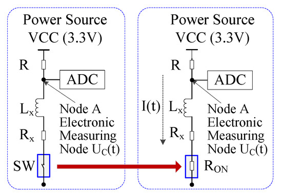
Figure 2.
Theoretical IPS measurement circuit in simulation (the resistance caused by the actual switching (SW) operation is considered).
In Figure 1, the target travels between the target and the coil, resulting in the change of the distance and the inductance . The value of affects the electronic measurement at Node A, which demonstrates the non-linear relationship to the physical target distance. By driving with a voltage source of and measuring at Node , the target distance can be provided. is the equivalent distributed capacitance; is the equivalent distributed inductance; is the current limitation resistance; is the resistance of the inductor.
However, when the resistances ( and ) are affected by the changing temperature, the electronic output signal at Node changes accordingly, which increases the deviation of the target distance estimation. Thus, due to the changing temperature, revisiting the IPS model is necessary.
In Figure 2, a 12 bit Analog-to-Digital Converter (ADC) is used with a power source VCC ( V). is the current limitation resistance; is the resistance of the inductor; and is the resistance of the switch. , , and are the Temperature Coefficients (TCs) of resistances , , and respectively, shown in Table 1. In this paper, the room temperature . is the current temperature, which changes from to in use. , , and are the typical values of , , and at room temperature, respectively, shown in Table 2. Based on the working voltage (), the limitation of dynamic power consumption (), and the current limitation of the low-power high-speed MOS switch, the working current of the coil is determined to be 12 mA, after which the current limiting resistance can be deduced as 250 . The coil is made of AWG41 wire (d = 0.071 mm), with a wire length of about 6 m, leading to an resistance of 22 at room temperature. Based on resistance of the 2N7002 transistor at room temperature and the working electrical parameters (the voltage between gate and source , the drain current ), after the actual test of the on-state voltage ( = 12 mA, = 0.444 V), is calculated as 3.7 .

Table 1.
Temperature Coefficients (TCs).
Table 2.
Typical resistance values.
2.2. Temperature Effect
2.2.1. Linear Change of Resistance
In the theoretical IPS measurement circuit of Figure 2, the resistance , , and change linearly with the temperature , shown in Equation (1). Due to this linear change of resistance, the output voltage at node also changes with the temperature.
2.2.2. Non-Linear Change of Voltage
The linear change of resistance with the temperature brings the non-linear change of the voltage . Thus, the changing temperature increases the computation deviation of distance estimation in linear LUT computation.
Besides the changing temperature, the computation amount is another necessary consideration in this paper. Equation (2) shows the solution of the classical system in Figure 1 [28]. It can easily be seen that has a complex non-linear relationship with temperature , which is too complex to be solved directly in ASIC. Because temperature is an important and necessary contributor in the IPS system, it is necessary to propose a simplified method for accurate online computation.
Sampling in Equation (2) at time and [28], we can obtain , as follows:
shows the same characteristic as regarding the temperature and computation amount. To analyze the temperature effect and computational complexity, we use two methods: the theoretical method for the model in Figure 2 and the linear LUT based method in [28].
The comparison between the computed by the theoretical method and the estimated by the LUT method in [28] when is shown in Figure 3. The average value of is 1.2 LSB, which causes the deviation of the voltage estimation.

Figure 3.
(a) Theoretical U1 and computed value of by the LUT method; (b) estimation deviation of the LUT method . The deviation (red area) and (yellow area) result in an incorrect voltage estimation. The LUT method shows a large estimation deviation at a low temperature.
In the red area of Figure 3b, when , . This means that is 0.5 LSB larger than , which results in an incorrect voltage estimation. In the green area, when and , . In this case, the estimated is very close to , which means the method [28] works correctly. In the yellow area, , . is −0.5 LSB less than , which also results in an incorrect voltage estimation. It can further be seen clearly in Figure 3 that the estimation deviation of is large at a low temperature, i.e., almost 8 LSB at .
The analysis shown in Figure 3 provides the temperature range for the proposed method in Section 3.2.2. Based on this analysis of the temperature range, the proposed method could purposefully increase the computation accuracy and reduce the amount of calculation.
2.2.3. Inductance Change
In addition to the above IPS internal parameters, the inductance , which is decided by the physical target distance, also influences the value of the measured voltage . The solution of the theoretical system in Figure 2 is as follows:
where is the measured voltage, whose value is related to the present estimated distance at current temperature . When the inductance changes from 4.5 mH to 5.5 mH, the simulation results show that the computation deviation between the theoretical value and the estimated by the LUT method is affected by the temperature, but not the distance-related parameter .
2.2.4. ADC and LDO Change
When measuring the voltage , we propose the following methods in the ADC circuit to reduce the influence of the temperature, shown in Figure 4.
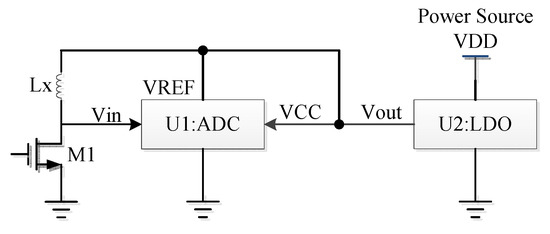
Figure 4.
Block diagram of the ADC and LDO circuit (we propose methods to reduce the influence of the temperature).
- The output voltage of the LDO supplies the voltage as the input voltage Vin of the ADC for the charge-discharge circuit of the IPS, the reference voltage VREF of the ADC, and the supply voltage VCC of the ADC. This kind of connection for the voltage supplies reduces the temperature effect on measuring .
- The ADC is redesigned with the optimized temperature coefficients for gain and offset.
The test results show that the deviations of and are about 2–3 LSB due to the circuit of the ADC and LDO when the temperature changes. The deviation caused by the circuit of the ADC and LDO is smaller than that by the resistances in Section 2.2.1. Moreover, the innovation of the ADC is another improvement activity in the analog field.
2.3. Summary of This Section
The conclusions drawn from the above analysis and simulation can be summarized as follows:
- The complexity of the equation requires a method with high accuracy, but not too much online computation work.
- The resistances , , and change linearly with the temperature , which results in the non-linear change of the voltages and the computation deviation of distance estimation.
- The inductance from 4.5 mH to 5.5 mH (or the target distance) has little effect on the computation deviation of .
- The temperature plays a significant role in computing and estimating the physical distance. The LUT based method in [28] largely simplifies the calculation, but produces a large estimation deviation at a low temperature.
3. Proposed Method
Due to the limitation of hardware resources, it is almost impossible to compute the and estimate the target distance directly using Equation (4). Although the linear measurement methods such as the LUT method in [28] could largely simplify the calculation, they produce a large estimation deviation due to the temperature effect, especially at a low temperature.
The overall goal of this study is to successfully realize a real-time and high-accuracy measurement method within a wide temperature range. The proposed method contains an offline and an online stage to achieve computation reduction, easy portability, robustness to the temperature changes, and easy ASIC implementation.
3.1. The Dual-Stage Scheme
The dual-stage scheme includes an offline stage and an online stage, as shown in Figure 5. The offline stage performs a large amount of computation based on the theoretical or measured voltages of and generates the temperature feature parameters , which are used in the online stage. Since these calculations do not exist in the ASIC, the amount of online calculation in the ASIC is significantly reduced with little hardware resource.

Figure 5.
Block diagram of the dual-stage scheme (the offline stage performs a large amount of computation and generates the temperature feature parameters, while the online stage predicts the target distance based on a non-linear piecewise fitting scheme with these parameters).
The online stage predicts the target distance based on a non-linear piecewise fitting scheme with the temperature feature parameters from the offline stage. Based on the voltages , introduced in Equation (3), the offline stage generates 5 temperature feature parameters for each distance . These parameters are stored in the system and used in the online stage.
In Figure 5, the subscript represents each distance point from 3 mm to 7 mm with a step of 0.04 mm.
3.2. The Offline Stage
3.2.1. The Temperature Feature Parameters
The temperature feature parameters represent the complex relationship between and , which can be calculated in an offline manner to reduce the amount of calculation and complexity of the ASIC. For each distance , the offline stage uses voltage pairs to calculate five feature parameters at six temperature points: , and .
To evaluate the algorithm comprehensively and objectively, two kinds of voltages are used in this paper: theoretical in the lab simulation step and the measured values in the practical application. All temperature feature parameters are stored as constants in the ASIC. Thus, the massive offline matrix calculus in the offline stage only uses the storage space in the ASIC, but it does not bring computational burden to the online stage.
Simulation results are introduced in Section 5.1, in which theoretical are generated by means of non-linear Equation (4). The ASIC results are presented in Section 5.2, in which the measured are actually measured voltage values.
3.2.2. Piecewise Fitting
According to Figure 3b, the estimated voltage of the linear method shows distinct characteristics regarding the temperature . The following can be obtained:
- When , the computed in the linear method exhibits a larger deviation from the theoretical value , indicating the obvious non-linear characteristic of the IPS system.
- When , the small deviation between and indicates the linear characteristic of the IPS system.
- at temperature points and indicates accurate voltage estimation.
According to the above conclusions, we propose a temperature based piecewise fitting scheme to compute the temperature feature parameters at the different temperature ranges according to their corresponding voltage deviation. With this fitting scheme, the proposed model can better represent the IPS measurement system when the temperature is changing, which could improve the estimation accuracy.
In the low temperature range of , the matrix calculus module computes the coefficients of a polynomial with a higher degree that is a best fit (in a least squares sense) for the data of . , , , and are the voltage values at a temperature of , , , and respectively; that is:
Moreover, in the temperature range of , the matrix calculus module computes with a lesser degree based on voltage pairs at and ; that is:
The matrix calculus module includes two parts: Vandermonde matrix construction and least squares problem calculation. The dimension of the Vandermonde matrix is , where represents the number of temperature points included and is the polynomial order plus one, as shown in Figure 6.
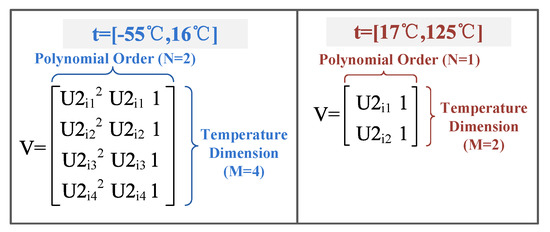
Figure 6.
Structure of the Vandermonde matrix (in the low temperature range of , the matrix module computes with a higher degree , while in the temperature range of , the matrix module computes with a lesser degree ).
The least squares problem calculation conducts the orthogonal-triangular decomposition, and it decomposes matrix into a product of an M-by-N upper triangular matrix and an M-by-N unitary matrix , so that . When , the polynomial coefficients in descending powers are computed by . When , the polynomial coefficients in descending powers are computed by .
Because the temperature feature parameters are calculated offline, the complexity of the computation does not increase the hardware resource consumption for the ASIC implementation. After moving all locations of the specified distance points , the offline stage generates the temperature feature parameters, as shown in Table 3.
Table 3.
Feature parameters at various .
3.3. The Online Stage
The introduced online stage aims to predict the target distance with high accuracy and minimal hardware consumption. By means of the non-linear piecewise computation, the online stage first generates the voltage pool of using the temperature feature parameters from the offline stage. Then, the online stage performs the online distance estimation, which predicts the target distance in real time with little storage resource.
3.3.1. Voltage Pool
Based on the temperature feature parameters, the online stage generates the voltage pool by means of the non-linear piecewise computation. The piecewise computation scheme performs both linear and non-linear polynomial calculations according to the temperature range, which could improve computation accuracy and reduce the unnecessary calculations simultaneously.
To better illustrate the piecewise computation scheme, we use the input of voltage group as the testing point, which is either computed by theoretical Equation (4) in simulation or measured in field tests. For each , based on the theoretical or measured voltage , the non-linear computation module computes the voltage pool of online by the pre-calculated , which uses the time-sharing hardware resources of four multipliers and three adders. These hardware resources are repeatedly used 101 times to cover the distance range of . At a low temperature range from to , the piecewise computation method computes the voltage pool with a higher degree based on . For the high temperature range of from to , the method computes with a lesser degree based on .
As illustrated in Equation (3), the voltage is only related to the temperature. According to the simulation results, we assume can represent the temperature range . Therefore, the online computation of the voltage pool for each time-sharing clip is as follows:
3.3.2. Distance Estimation
The distance estimation module chooses the voltage value from the voltage pool of that is closest to the current measured , and the sequence number of this chosen voltage represents the estimated distance .
Specifically, the distance estimation module computes the deviation of and compares with the previously stored . If , is replaced by ; otherwise, is kept unchanged. The initial value of is defined as . The distance mark is the sequence number of . After 101 cycles, the scheme outputs the distance mark and its corresponding distance value . In other words, the distance estimation module searches from , which are computed online based on the input of , and then finds the value that is nearest to the input of .
3.4. Summary of This Section
To achieve high accuracy and easy ASIC implementation, the proposed method adopts the following:
- The dual-stage scheme: This scheme includes an offline stage and an online stage, which enables computation reduction, flexible application, strong temperature adaptability, and easy ASIC realization.
- The offline calculation of the temperature feature parameters: These parameters can be calculated in an offline manner to reduce the amount of calculation and complexity significantly when computing and under the changing temperature.
- The piecewise fitting scheme: This scheme performs the piecewise fitting at the different temperature ranges according to their corresponding voltage deviation, which makes the proposed model close to the IPS measurement system when the temperature is changing.
- The voltage pool generated by the online piecewise computation: The online stage generates the voltage pool by means of the non-linear piecewise computation. The temperature based piecewise computation performs both linear and non-linear polynomial online calculation according to the temperature range, which could improve the computation accuracy and reduce the unnecessary calculation simultaneously.
- The distance estimation: By choosing the optimal voltage value, the proposed model can predict the target distance in real time.
Considering the non-linear characteristic of the IPS measurement system with the change of temperature, the proposed method could successfully achieve real-time and high-accuracy target estimation under the changing temperature with low hardware resource consumption. The simulation and ASIC results are shown in Section 5.
4. ASIC Implementation
Based on the stage technology of the proposed algorithm, this product was already released in 2019 for industrial fields such as landing gears.
This product is implemented in an Analog Digital (AD) mixed CMOS integrated circuit, which includes the digital stage of the proposed algorithm, the Electrically Erasable Programmable Read Only Memory (EEPROM), the Low Dropout Regulator (LDO), the ADC interface logic, and the Power On Reset (POR) circuit, as shown in Figure 7.
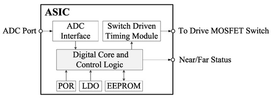
Figure 7.
Functional block diagram of the ASIC (AD mixed CMOS integrated circuit).
The die layout in Figure 8a mirrors the schematic representation of the architecture. Figure 8b is a die micrograph. The die size is .
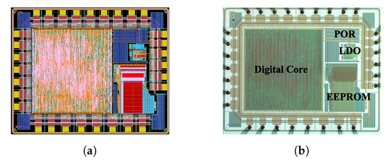
Figure 8.
(a) Layout; (b) die micrograph. The die size is 3.2 mm × 2.7 mm.
The ASIC chip is fabricated in the 0.18 m CMOS process and encapsulated in a 40-pin CQFN, (Figure 9a). This chip is mounted on a PCB circuit as a core component (Figure 9a), which is then integrated into the evaluation PCB board (Figure 9b).
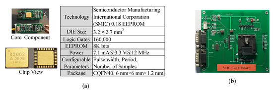
Figure 9.
(a) Chip info (the ASIC chip is fabricated in the 0.18 μm CMOS process and encapsulated in a 40-pin CQFN); (b) evaluation PCB board (the size of the board is 10 mm × 25 mm).
5. Results and Discussion
Both the theoretical simulation and ASIC results are conducted to evaluate the accuracy of the proposed model in this section. It is noted that the inductance , instead of the distance , is used in the theoretical mode (Figure 2) and is inversely proportional to , thus making an appropriate metric in the theoretical simulation.
5.1. Simulation Results
As shown in (Figure 2), the value of changes when the target travels, resulting in the change of . Therefore, we evaluate and in the theoretical simulation of this subsection.
5.1.1. Simulation of
First, the intermediate variable is analyzed in the simulation. We use the difference of the voltage to evaluate the performance of the proposed model. Specifically, we define as the difference between of the theoretical Equation (4) and of the LUT method [28] and as the difference between of the theoretical Equation (4) and of the method proposed in this paper, such that:
When the target moves in the IPS system, the inductance changes accordingly. Here, the subscript represents the sequence of inductance from 4.5 mH to 5.5 mH with a step of 0.01 mH and the subscript represents the temperature range from to with a step of . To analyze the calculation accuracy of , and are shown in Figure 10. The shape of is curved from −1.297 LSB to 8.666 LSB. The shape of is almost a plane of zero value, whose range is LSB. is much less than , which demonstrates that the proposed model reduces the estimated deviation of . At each temperature point, the maximum of with different is 0.084 LSB, whereas this value is 0.042 LSB for . Thus, the estimated deviation of caused by the changing inductance is minimal and can be ignored. Table 4 lists the detailed data analysis of and . is reduced by about two orders of magnitude of .
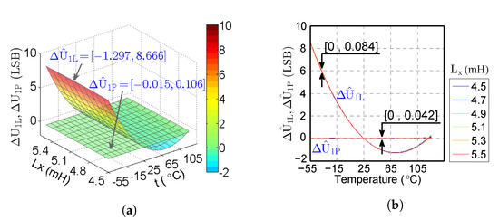
Figure 10.
and with different displayed by: (a) 3D map (the estimated deviation of our method is much less than the deviation by LUT, especially at a low temperature); (b) 2D map (at each temperature point, the maximum of is less than with different ).
Table 4.
Comparison of statistical values and (the computed by our method are closer to the theoretical than by the LUT method).
Therefore, we can conclude that all the computed are closer to the theoretical than for all in the simulation, and thus, the proposed model improves the calculation accuracy of over the LUT method in the theoretical simulation.
5.1.2. Simulation of
Based on the calculation of the voltage , the output inductance of can be estimated. When the inductance changes from 4.5 mH to 5.5 mH with a step of 1 H and the temperature changes from to with a step of in the simulation, the number of test cases is 181,181. Equation (9) illustrates the computed inductance and , that is:
where the subscript represents the sequence of inductance, the subscript represents the sequence of temperature, is the theoretical inductance value, is the estimated inductance by the LUT method, and is the estimated value by the proposed method.
In Figure 11, H and H, which demonstrates that the deviation of the computed inductance is reduced obviously. As can be seen in Figure 11, exhibits a large deviation under the low temperature range. In Figure 11b, the green areas indicate the correct computation that , and the red areas indicate the incorrect computation that . Since all the areas in Figure 11d are green, the proposed method can obtain correct results for all the estimations. Compared to the LUT method, the proposed model can reduce the error rate from 84.3% to 0%, which demonstrates the effectiveness of the proposed model for the whole temperature range.
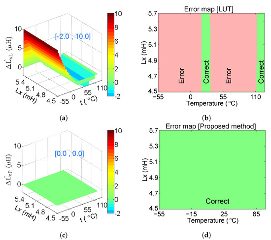
Figure 11.
(a) with different ( exhibits a large deviation under the low temperature range); (b) error map of (the green areas indicate the correct computation that and the red areas indicate the incorrect computation that ); (c) with different ( demonstrates that the deviation is reduced obviously); (d) error map of (all the areas are green, indicating that the proposed method can obtain correct results for all the estimations).
5.2. ASIC Results
When using the IPS measurement system, the distance is the final output, so we evaluate and the distance in the field experiments. In this subsection, the target is moved within the distance range of [3 mm, 7 mm] with a step of 0.04 mm for each temperature point. All the voltage values in this subsection are measured online from the evaluation PCB board (Figure 9b).
5.2.1. ASIC Results of
First, the intermediate variable is analyzed in the ASIC results. Based on the measured voltage , and denote the voltage computed by the LUT method and the proposed method, respectively. The difference between the measured and the computed of the LUT method [28] is defined as . The difference between the measured and the computed of the proposed method is defined as , shown as:
where the subscript represents the sequence of the target distance from 3 mm to 7 mm with a step of 0.04 mm and the subscript represents the temperature from to with a step of .
The proposed method generates more accurate estimated values, as clearly seen at a low temperature in Figure 12. The range of is [−43.418, 5.995] LSB and is [−5.893, 5.933] LSB, so is much less than . The values of the colormap from top (−50) to bottom (10) are mapped to colors from dark blue through green to red, which is centered at zero to be colored green. The blue color of the areas at a low temperature in Figure 12a,b changes to green color in Figure 12c,d, which indicates that is closer to zero than . We also show the covered curves of and for each distance in Figure 13. At a low temperature, of the proposed method is closer to zero than , which demonstrates that the proposed system can obtain more accurate calculation of .
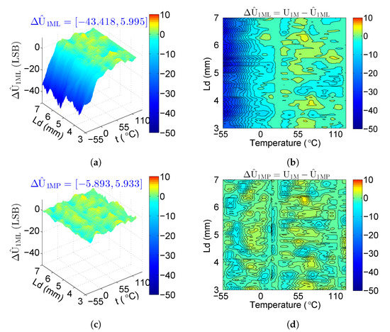
Figure 12.
with different displayed by: (a) 3D map; (b) contour map; with different displayed by: (c) 3D map; (d) contour map (the blue color of the areas at a low temperature in (a,b) changes into green color in (c,d), which indicates that is closer to zero than ).
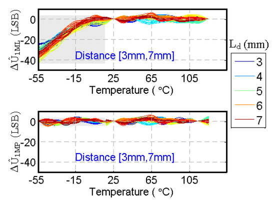
Figure 13.
and with different (at a low temperature, of the proposed method is closer to zero than , which demonstrates that the proposed system can obtain more accurate calculation of ).
Table 5 presents the detailed data analysis of and . The values of are much less than , especially the minimum values, thereby demonstrating that the proposed system can obtain more accurate distance estimation for all the cases, especially at a low temperature.
Table 5.
Comparison of statistical values and (the values of are much less than , especially the minimum values, thereby demonstrating that the proposed system can obtain more accurate distance estimation).
5.2.2. ASIC Results of
The estimated distance is the output of the IPS measurement system. Moving the target distance from 3 mm to 7 mm with a step of 0.04 mm, the estimated distance by the LUT method and the proposed method is computed, respectively.
The difference between the target distance and of the LUT method [28] is defined as . The difference between and of the method proposed in this paper is defined as , which can be shown as:
where the subscript represents the sequence of the target distance from 3 mm to 7 mm with a step of 0.04 mm and the subscript represents the temperature from to with a step of .
Figure 14 presents the differences of distance estimation ( and ). The range of is [−2.1, 0.4] mm, and the range of is [−0.5, 0.4] mm, which shows that the proposed system can decrease the deviation of the distance estimation. Values of the colormap from top (−2.4) to bottom (0.8) are mapped to colors from dark blue through green to red, which is centered at zero to be colored green. The blue color of the areas at a low temperature in Figure 14a,b changes into green color in Figure 14d,e, which indicates that is closer to zero than . Moreover, we set a 0.4 mm deviation tolerance for the correct distance estimation, which means the method works correctly when . In Figure 14c,f, the green areas indicate the correct distance estimation, and the red areas indicate the incorrect distance estimation. The error rate is reduced from 23.5% (Figure 14c) to 4.1% Figure 14f. It can thus be concluded that the proposed system can improve the accuracy of distance estimation for the whole temperature range.
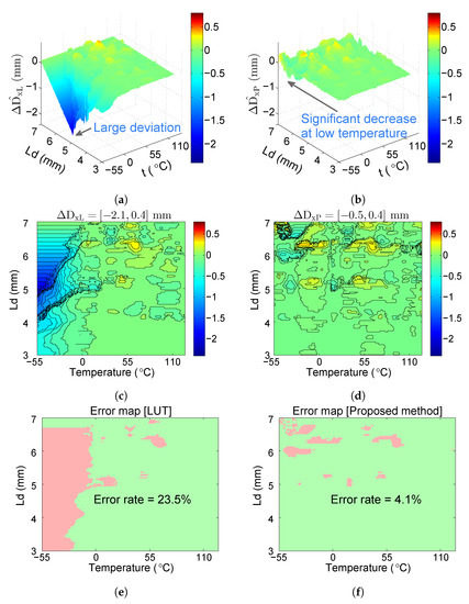
Figure 14.
(a) displayed by 3D map (the value of is about −2.1 mm at a low temperature, which indicates the large distance deviation of the LUT method); (b) displayed by 3D map (the value of is close to zero mm at a low temperature, which shows that the proposed system can decrease the deviation of the distance estimation); (c) displayed by contour map ( is in the range of [−2.1, 0.4] mm, the large negative value of which results in the blue color of the areas at a low temperature); (d) displayed by contour map (the blue color of the areas at a low temperature in (c) changes into green color in (d), which indicates that is closer to zero than ); (e) error map of (the error rate of the LUT method is 23.5%); (f) error map of (the error rate of our proposed method is 4.1%).
In our ASIC application, the most commonly used sensing distance is 4 mm. Figure 15 plots the estimated distance for 4 mm at different temperatures. At , when the target distance is 4 mm, the LUT method provides an incorrect distance estimation of 4.84 mm due to the interference of the low temperature. By contrast, the proposed method eliminates the effects of temperature, the estimated distances of which fall within the range of .

Figure 15.
and of 4 mm (the red curve of provides an incorrect distance estimation at a low temperature; by contrast, the blue curve of falls within the range of ).
In Table 6, all estimated distances are within the range of [3.8, 4.2] mm with an average estimation of 4.034 mm, which demonstrates that a more accurate sensing distance has been obtained by the proposed system.
Table 6.
Comparison of the estimated distances when the target distance is 4 mm ( are closer to 4 mm than , and all the values of are within the range of [3.8, 4.2] mm, which demonstrates that a more accurate sensing distance was obtained by the proposed system).
We present the performance summary and comparison with some publicly released references, which have the same application background in the field of aviation, shown in Table 7. The linear computation methods are used and only the simulation results are shown for [28,29]. The ASIC chips are implemented for [30] and our proposed method. The typical distance deviation of chips is decreased from 0.4 mm [30] to 0.12 mm, which demonstrates that the proposed system can obtain a more accurate sensing distance.
Table 7.
Performance summary and comparison with previous work.
6. Conclusions
IPS suffers from temperature changes, which significantly decrease the measurement accuracy at low temperatures. Many proposed methods such as [27,28] achieve high accuracy at room temperature, but show large deviation at low temperatures. To improve the robustness for the temperature changing, we adopt the non-linear temperature compensation model, rather than the simple linear LUT method, to provide more accurate distance estimation within a wide temperature range compared to the previous work.
The innovations for high-accuracy measurement always increase the complexity of the ASIC implementation in the industrial fields, due to the limitation of hardware resources. We propose a serial dual-stage scheme to reduce the amount of online calculation and enable easy ASIC implementation, in which the offline stage performs a large amount of the computation and the online stage predicts the target distance with little hardware resource. Since the large amount of the parameter computation can be performed in the offline stage, the proposed system can guarantee both high accuracy and easy ASIC implementation.
This model is fabricated in a 0.18 m CMOS process and packaged in a CQFN40. For the most commonly used sensing distance of 4 mm, the computed distance deviation of our ASIC chips falls within the range of mm in the temperature range from to , which demonstrates that the presented model could successfully achieve real-time and high-accuracy computation within a wide temperature range with low hardware resource consumption.
Author Contributions
L.W. proposed the original idea, carried out the simulation, and completed the ASIC tests; H.-B.T. designed the ASIC chips; H.D. proofread the formats; Z.-B.S. and F.W. proposed the research direction. All authors contributed to the organization of the paper, writing, and proofreading. All authors read and agreed to the published version of the manuscript.
Funding
This research received no external funding.
Conflicts of Interest
The authors declare no conflict of interest.
Abbreviations
The following abbreviations are used in this manuscript:
| IPS | Inductive Proximity Sensor |
| LUT | Look-Up Table |
| CMOS | Complementary Metal Oxide Semiconductor |
| ASIC | Application-Specific Integrated Circuit |
| TC | Temperature Coefficient |
| PCB | Printed Circuit Board |
| LSB | Least Significant Bit |
| ADC | Analog-to-Digital Converter |
| AD | Analog Digital |
| EEPROM | Electrically Erasable Programmable Read only Memory |
| LDO | Low Dropout Regulator |
| POR | Power On Reset |
References
- Grandi, G.; Massarini, A.; Reggiani, U.; Sancineto, G. Laminated iron-core inductor model for time-domain analysis. In Proceedings of the 4th IEEE International Conference on Power Electronics and Drive Systems, Denpasar, Indonesia, 25 October 2001; pp. 680–686. [Google Scholar] [CrossRef]
- De Leon, F.; Semlyen, A. Time domain modeling of eddy current effects for transformer transients. IEEE Trans. Power Deliv. 1993, 8, 271–280. [Google Scholar] [CrossRef]
- Agrawal, D.P. Embedded Sensor Systems; Springer: Singapore, 2017. [Google Scholar]
- Zheng, D.; Zhang, S.; Wang, S.; Hu, C.; Zhao, X. A Capacitive Rotary Encoder Based on Quadrature Modulation and Demodulation. IEEE Trans. Instrum. Meas. 2015, 64, 143–153. [Google Scholar] [CrossRef]
- Sun, B.; Li, B. Laser Displacement Sensor in the Application of Aero-Engine Blade Measurement. IEEE Sens. J. 2016, 16, 1377–1384. [Google Scholar] [CrossRef]
- Matsui, Y.; Akagi, T.; Dohta, S. Development of low-cost wire type linear potentiometer for flexible spherical actuator. In Proceedings of the 2016 IEEE International Conference on Advanced Intelligent Mechatronics (AIM), Banff, AB, Canada, 12–15 July 2016; pp. 1017–1021. [Google Scholar] [CrossRef]
- Nauduri, B.S.; Shaga, G. A novel approach of using a planar inductive position sensor for the Permanent magnet synchronous motor control application. In Proceedings of the 2018 IEEE Sensors Applications Symposium (SAS), Seoul, Korea, 12–14 March 2018; pp. 1–5. [Google Scholar] [CrossRef]
- Chlenova, A.A.; Moiseev, A.A.; Derevyanko, M.S.; Semirov, A.V.; Lepalovsky, V.N.; Kurlyandskaya, G.V. Permalloy-Based Thin Film Structures: Magnetic Properties and the Giant Magnetoimpedance Effect in the Temperature Range Important for Biomedical Applications. Sensors 2017, 17, 1900. [Google Scholar] [CrossRef] [PubMed]
- Aschenbrenner, B.; Zagar, B.G. Analysis and Validation of a Planar High-Frequency Contactless Absolute Inductive Position Sensor. IEEE Trans. Instrum. Meas. 2015, 64, 768–775. [Google Scholar] [CrossRef]
- Babu, A.; George, B. Design and Development of a New Non-Contact Inductive Displacement Sensor. IEEE Sens. J. 2018, 18, 976–984. [Google Scholar] [CrossRef]
- Position Sensors for Safety Applications. Celera Motion. USA. 12 December 2019. Available online: https:www.zettlex.com/articles/position-sensors-for-safety-applications (accessed on 15 July 2020).
- Inductive Positioning Systems. Baluff. Germany. 12 December 2019. Available online: https://www.balluff.com.cn/local/us/productfinder/#/ca/A0001/cg/G0101/product/F01110 (accessed on 15 July 2020).
- Proximity Sensors. Honeywell. USA. 6 January 2020. Available online: https://sensing.honeywell.com/sensors/proximity-sensors (accessed on 15 July 2020).
- Proximity Sensing Systems Overview. Crane Aerospace & Electronics. USA. 12 December 2019. Available online: http:www.craneae.com/Products/Sensing/ProximitySystemsOverview.aspx (accessed on 15 July 2020).
- Rana, S.; George, B.; Kumar, V.J. An Efficient Digital Converter for a Non-Contact Inductive Displacement Sensor. IEEE Sens. J. 2018, 18, 263–272. [Google Scholar] [CrossRef]
- Rana, S.; George, B.; Jagadeesh Kumar, V. Self-Balancing Signal Conditioning Circuit for a Novel Noncontact Inductive Displacement Sensor. IEEE Trans. Instrum. Meas. 2017, 66, 985–991. [Google Scholar] [CrossRef]
- Reverter, F.; Gasulla, M. Timer-Based Demodulator for AM Sensor Signals Applied to an Inductive Displacement Sensor. IEEE Trans. Instrum. Meas. 2017, 66, 2780–2788. [Google Scholar] [CrossRef]
- Tang, Q.; Wu, L.; Chen, X.; Peng, D. An Inductive Linear Displacement Sensor Based on Planar Coils. IEEE Sens. J. 2018, 18, 5256–5264. [Google Scholar] [CrossRef]
- Sandra, K.R.; Kumar, A.S.A.; George, B.; Kumar, V.J. A Linear Differential Inductive Displacement Sensor With Dual Planar Coils. IEEE Sens. J. 2019, 19, 457–464. [Google Scholar] [CrossRef]
- Switches and Position Sensors. Crouzet. France. 12 December 2019. Available online: http:www.crouzet-aerospace.com/productlines/detection-and-sensing (accessed on 15 July 2020).
- Wilson, P.R.; Ross, J.N.; Brown, A.D. Simulation of magnetic component models in electric circuits including dynamic thermal effects. IEEE Trans. Power Electron. 2002, 17, 55–65. [Google Scholar] [CrossRef]
- Danisi, A.; Masi, A.; Losito, R. Performance Analysis of the Ironless Inductive Position Sensor in the Large Hadron Collider Collimators Environment. Sensors 2015, 15, 28592–28602. [Google Scholar] [CrossRef] [PubMed]
- Podhraški, M.; Trontelj, J. A Differential Monolithically Integrated Inductive Linear Displacement Measurement Microsystem. Sensors 2016, 16, 384. [Google Scholar] [CrossRef] [PubMed]
- Cai, J.; Lu, L.; Liu, Z.; Jia, H.; Zhao, X.; Xu, F. An inductive position sensor with switched reluctance motor structure. In Proceedings of the 2017 20th International Conference on Electrical Machines and Systems (ICEMS), Sydney, Australia, 11–14 August 2017; pp. 1–4. [Google Scholar] [CrossRef]
- Nabias, J.; Asfour, A.; Yonnet, J.P. Temperature effect on GMI sensor: Comparison between diagonal and off-diagonal response. Sens. Actuators Phys. 2019, 289, 50–56. [Google Scholar] [CrossRef]
- Matko, V.; Milanović, M. High-Precision Hysteresis Sensing of the Quartz Crystal Inductance-to-Frequency Converter. Sensors 2016, 16, 995. [Google Scholar] [CrossRef] [PubMed]
- Guo, Y.X.; Shao, Z.B.; Li, T. An Analog-Digital Mixed Measurement Method of Inductive Proximity Sensor. Sensors 2016, 16, 30. [Google Scholar] [CrossRef] [PubMed]
- Guo, Y.X.; Shao, Z.B.; Tao, H.B.; Xu, K.L.; Li, T. Dimension-Reduced Analog-Digital Mixed Measurement Method of Inductive Proximity Sensor. Sensors 2017, 17, 1533. [Google Scholar] [CrossRef] [PubMed]
- Guo, Y.X.; Lai, C.; Shao, Z.B.; Xu, K.L.; Li, T. Differential Structure of Inductive Proximity Sensor. Sensors 2019, 19, 2210. [Google Scholar] [CrossRef] [PubMed]
- Huang, W.; Wang, C.; Liu, L.; Huang, X.; Wang, G. A signal conditioner IC for inductive proximity sensors. In Proceedings of the 2011 9th IEEE International Conference on ASIC, Xiamen, China, 25–28 October 2011; pp. 141–144. [Google Scholar] [CrossRef]


© 2020 by the authors. Licensee MDPI, Basel, Switzerland. This article is an open access article distributed under the terms and conditions of the Creative Commons Attribution (CC BY) license (http://creativecommons.org/licenses/by/4.0/).