Article

Post-Voltage-Boost Circuit-Supported Single-Ended Class-B Amplifier for Piezoelectric Transducer Applications

1
Department of Biomedical Engineering, Gachon University, 191 Hambakmoe-ro, Yeonsu-Gu, Incheon 21936, Korea
2
Department of Medical IT Convergence Engineering, Kumoh National Institute of Technology, 350-27 Gumi-daero, Gumi 39253, Korea
*
Author to whom correspondence should be addressed.
These authors contributed equally.
Sensors 2020, 20(18), 5412; https://doi.org/10.3390/s20185412
Submission received: 27 August 2020 / Revised: 7 September 2020 / Accepted: 14 September 2020 / Published: 21 September 2020
(This article belongs to the Special Issue Ultrasound Imaging and Sensing)

Abstract

:
Piezoelectric transducers are important devices that are triggered by amplifier circuits in mobile ultrasound systems. Therefore, amplifier performance is vital because it determines the acoustic piezoelectric transducer performances. Particularly, mobile ultrasound applications have strict battery performance and current consumption requirements; hence, amplifier devices should exhibit good efficiency because the direct current (DC) voltage in the battery are provided to the supply voltages of the amplifier, thus limiting the maximum DC drain voltages of the main transistors in the amplifier. The maximum DC drain voltages are related with maximum output power if the choke inductor in the amplifier is used. Therefore, a need to improve the amplifier performance of piezoelectric transducers exists for mobile ultrasound applications. In this study, a post-voltage-boost circuit-supported class-B amplifier used for mobile ultrasound applications was developed to increase the acoustic performance of piezoelectric transducers. The measured voltage of the post-voltage-boost circuit-supported class-B amplifier (62 VP-P) is higher than that of only a class-B amplifier (50 VP-P) at 15 MHz and 100 mVP-P input. By performing the pulse-echo measurement test, the echo signal with the post-voltage-boost circuit-supported class-B amplifier (10.39 mVP-P) was also noted to be higher than that with only a class-B amplifier (6.15 mVP-P). Therefore, this designed post-voltage-boost circuit can help improve the acoustic amplitude of piezoelectric transducers used for mobile ultrasound applications.

1. Introduction

Piezoelectric transducers have been widely utilized for a variety of ultrasound components, such as touch-pad smartphone and parking assistance sensors, pulse-echo measurement instruments, nondestructive testing systems, submarine radar devices, material characterization systems, and acoustic trapping devices [1,2,3,4,5]. The transducers generate acoustic waves triggered by electrical power or waves stimulated by acoustic forces [6]. The primary capacitance with parasitic resistance, capacitance, and inductance in the transducer equivalent circuit model represent non-linear characteristics because the transducer is sensitive to voltage and frequency variances [7]. The maximum alternative current (AC) applied voltages to the piezoelectric material must be less than maximum DC applied voltages to the piezoelectric material [8,9]. Within limited DC applied voltages, higher applied voltages could produce higher acoustic amplitude generated from the transducer [10,11]. The applied voltage with different frequencies ranging between resonant and anti-resonant frequencies, owing to unmatched impedance conditions, could generate lower or very weak acoustic waves [8]. As a result, ensuring the proper design of electronic devices is key to attaining piezoelectric transducers with stable performance. In electronic devices, amplifiers are among the electronic devices that most significantly affect the sensitivity performance of ultrasound systems [12]. They are also considered final-stage electronics, with the exception of expander circuits, which are required for piezoelectric transducers with high voltage amplitude waveform [13]. In ultrasound applications, the amplifier is usually employed to amplify a variety of pure sine, square, or coded signals depending on the ultrasound imaging modes [14,15,16]. These signals are typically generated from digital signal processing or field-programmable gate array (FPGA) electronics, after which they are transmitted to piezoelectric transducers to produce sensitive vibrational waves [17].
Currently, the applications of mobile ultrasound are increasing in the fields of touch-pad smartphones and mobile medical instruments [18,19]. However, these systems are normally required to have miniaturized piezoelectric transducers compared to large bench-top systems [8,18,20,21,22]. Therefore, some small-size piezoelectric transducers have limited maximum direct current (DC) applied voltages. For 4 × 4 × 4-mm3 PMN-PZT piezoelectric material, the measured maximum DC applied voltages are approximately 150 VP-P [12,23]. The maximum applied DC voltage restricts the maximum alternating current (AC) voltages for amplifiers in mobile systems [24,25,26]. Thus, maximum AC voltages that are less than DC voltages can directly trigger the piezoelectric transducers. The amplifiers with higher AC voltages are more useful, especially for mobile ultrasound systems [27]. In fact, ultrasound companies tried to apply much lower AC voltages to reduce heat effects to the transducers, thus reducing the sensitivity performances. The amplifiers with higher AC voltages and efficiency are more desirable. For example, in mobile ultrasound systems, piezoelectric array-type transducers that are smaller than 1 × 1 × 1 mm3 can be utilized. For most mobile ultrasound systems owing to space limitations, the smaller size piezoelectric transducers can be utilized [28,29]. Therefore, amplifier performance improvement in mobile ultrasound systems is beneficial to produce high acoustic amplitudes.
Several electronics research works have focused on improving the amplifier performance for piezoelectric transducer applications. The Texas Instruments medical device group developed a pre-distortion technique using analog-to-digital converters (ADCs), digital-to-analog-converters (DACs), memory, and FPGA electronics for ultrasound applications [30]. This scheme is useful for a single ultrasonic transducer and class-A amplifier, which are required to possess high power consumption in the bench-top ultrasound machines. The pre-linearizer is supposed to be placed before the amplifier circuit [31,32,33]. However, the post-distortion linearizer circuit is located between the amplifier and piezoelectric transducer or between the expander after the amplifier and piezoelectric transducer [34,35]. Likewise, using a similar circuit type after the amplifier could easily enable the controlled performance of the piezoelectric transducer because this circuit is located between the amplifier and transducer. Therefore, the placement of the circuit before piezoelectric transducers may be more useful because they have some unwanted parasitic capacitance, inductance, and resistance, such that similar circuit types could be further customized between the amplifier and piezoelectric transducers. A post-distortion linearizer circuit was developed for a class-A amplifier and intended for bench-top ultrasound instrument applications [34]. This approach helps achieve a flatter gain within wide input power ranges for a class-A power amplifier required to have high power consumption.
However, our proposed scheme is intended to increase the voltage output for a class-B amplifier, thus, improving the acoustic waveform amplitude for mobile ultrasound systems with limited DC voltages. Nonlinear amplifiers such as the class-B amplifier are preferable for mobile ultrasound instruments owing to their lower DC power consumption [19]. For typical ultrasound applications, a single-ended-type class-B amplifier is preferable compared to a differential-ended amplifier for piezoelectric transducers, because some piezoelectric transducers have large undesirable capacitances in their equivalent circuit models [36,37,38]. A differential-ended amplifier scheme can change the resonant frequency of piezoelectric transducers because the change from a differential path to a single path requires the use of large inductive-type transformers [39,40]. In addition, mobile systems have limited DC power consumption owing to their battery capacity, such that electronic device performance is also affected when designing transducer devices [8,41,42,43].
In this study, we first implemented a post-voltage-boost circuit-supported by a single-ended class-B amplifier for piezoelectric transducers. Figure 1 shows the concept of the proposed post-voltage-boost circuit for the class-B amplifier and piezoelectric transducer applications. As shown in Figure 1a,b, the post-voltage-boost circuit is located between the class-B amplifier and piezoelectric transducer, enabling the performance control of the class-B amplifier and piezoelectric transducer. Therefore, the output voltage of the post-voltage-boost circuit-supported class-B amplifier can be varied such that the echo signal amplitude of the piezoelectric transducer can be affected as well, as shown in Figure 1a.
Section 2 describes the operational mechanism, circuit schematic diagram, and mathematical analysis of the designed post-voltage-boost circuit and single-ended class-B amplifier. Section 3 demonstrates the improved electrical and acoustic performance of the designed electronic devices using a piezoelectric transducer with respect to the electronic measurement. Finally, Section 4 concludes the paper.

2. Materials and Methods

There are two different types of ultrasonic transducers, namely the capacitive micromachined ultrasonic transducer (CMUT), which is driven by a current signal, and the piezoelectric transducer, which is driven by a voltage signal [4]. A piezoelectric transducer was used for this research. The high voltage signal output from the amplifier is transmitted to the piezoelectric transducer [44,45]. Higher output voltage amplitude from the amplifier is transmitted to obtain higher acoustic signal amplitude generated from the piezoelectric transducer [28,46,47]. Thus, a stronger acoustic signal can be achieved from piezoelectric transducers [8,12]. Therefore, a post-voltage-boost circuit was designed to obtain a higher acoustic signal from piezoelectric transducers. The output signal of a single-ended class-B amplifier is transferred to the input of the post-voltage-boost circuit. The received signal from the amplifier is modulated in the post-voltage-boost circuit.

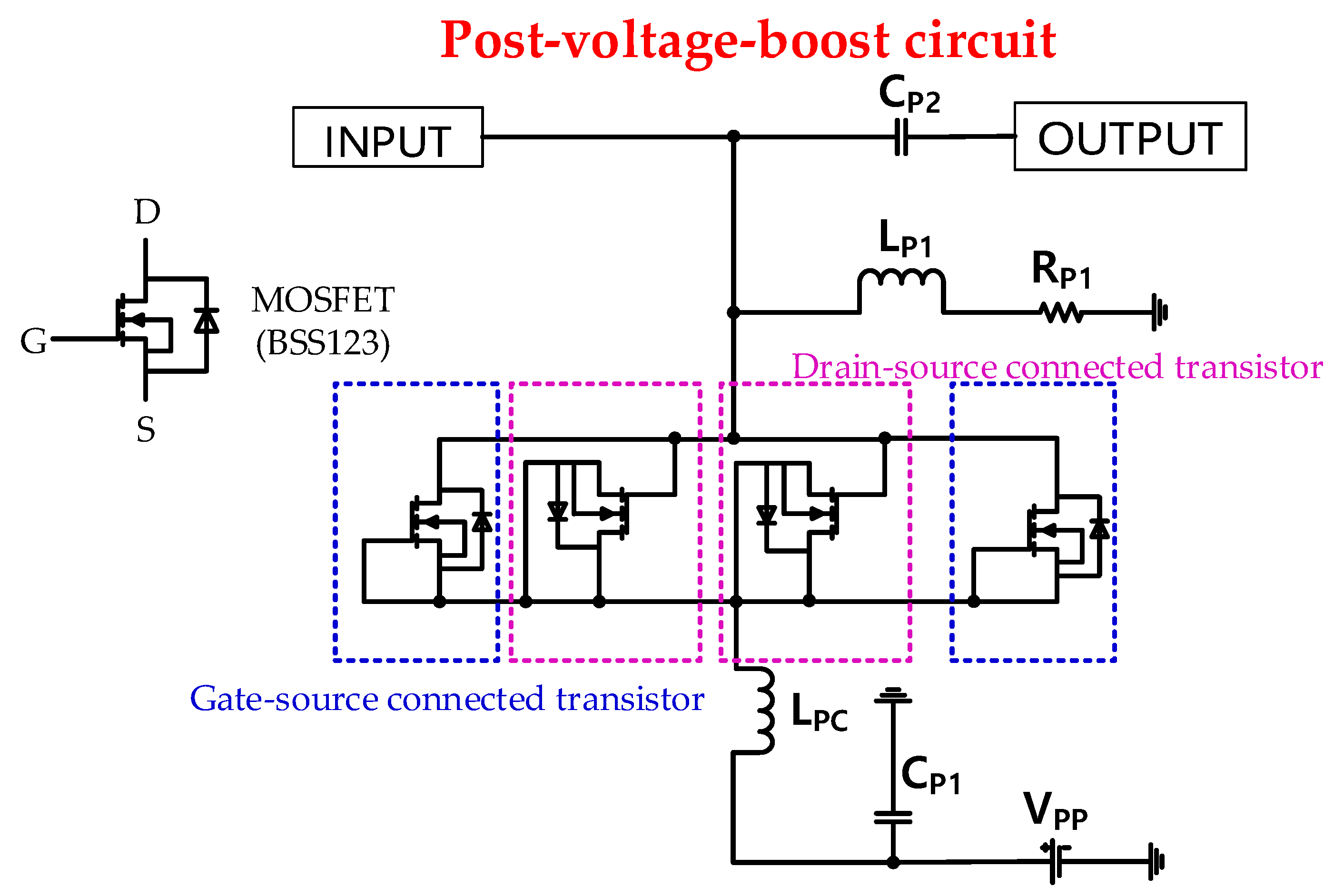
2.1. Schematic of Class-B Amplifier and Post-Voltage-Boost Circuit

In Figure 2, a schematic of a single-ended two-stage class-B amplifier with a post-voltage-boost circuit shows the operational mechanisms. In this amplifier, a power metal-oxide-semiconductor field-effect transistor (power MOSFET, PD57018-E, STMicroelectronics Corp., Geneva, Switzerland) was used as the main transistor. The first- and second-stage amplifiers were applied with a 3.1-V gate bias voltage to be operated in the class-B mode. The inductors at the gate and drain sides are choke inductors (LC = 1 μH), which could minimize the voltage drop when DC bias voltages were used [48,49,50]. In addition, the electrolytic capacitors (CG1, CD3, CG6, and CD8 = 220 μF) and ceramic capacitors (CG2, CD2, CG7, and CD7 = 1000 pF, CG3, CD1, CG8, and CD6 = 47 pF) were used to minimize the noise signals from the DC power supply [51,52]. The input inductors, capacitors, and resistors (LG1 and LG3 = 22 nH, CG4 and CG9 = 560 pF, CG5 and CG10 = 330 pF, LG2 and LG4 = 1000 nH, and RG3 and RG6 = 200 Ω), and output inductors, capacitors, and resistors (LD1 and LD3 = 120 nH, CD4 and CD9 = 330 pF, CD5 and CD10 = 820 pF, LD2 and LD4 = 500 nH, and RD1 and RD2 = 200 Ω) in the first- and second-stage class-B amplifiers were configured for 50 Ω impedance matching conditions at a center frequency of 15 MHz.
Figure 3 shows a schematic of the post-voltage-boost circuit. The post-voltage-boost circuit input (INPUT) is connected from the amplifier output (OUTPUT), as shown in Figure 2. Thus, the output signal of the amplifier (OUTPUT) is transmitted to the input (INPUT) of the post-voltage-boost circuit, as shown in Figure 3. The post-voltage-boost circuit consists of a DC bias signal input (VPP), electrolytic capacitor (CP1 = 220 μ F), choke inductor (LPC = 1   μ H), four transistors, inductor (LP1 = 2.2 μ H), resistor (RP1 = 50 Ω), and capacitor (CP2 = 220 pF). In the post-voltage-boost circuit, the four transistors are the gate-source or drain-source connected type. Gate-source connected transistors can be interpreted as variable resistors, and drain-source connected transistors can be interpreted as variable capacitors in the equivalent circuit model [24,41]. The gate-source or drain-source connected transistors behave as variable resistors or capacitors depending on the applied bias DC voltage of the post-voltage-boost circuit. Because the designed class-B amplifier is operated under a high-voltage and high-current environment, it is designed to be stable in that environment using four MOSFETs in a post-voltage-boost circuit. The four MOSFETs were selected due to high voltage and high current environment. Therefore, in the theoretical approaches, the parasitic resistance of four MOSFETs are reduced by ¼ times of one MOSFET, but the parasitic capacitance of four MOSFETs are increased by 4 times of one MOSFET. Therefore, the variable capacitors and resistors, which depend on the applied DC bias voltages (VPP), could offset the variances of the inductors (LD3 and LD4) and capacitors (CD10 and CD9), including the large unwanted parasitic capacitances of the power MOSFET in the second-stage amplifier. In addition, unnecessary harmonic signals that are generated from the amplifier can be reduced using a resonance filter structure in the post-voltage-boost circuit (CP2, LP1, and RP1) [53,54,55,56].

2.2. Equivalent Circuit Analysis of Class-B Amplifier

A two-stage class-B amplifier can be estimated by performing an equivalent circuit analysis. To simplify the equivalent circuit analysis, the internal resistance and inductance values of the transistors at each stage (gate, drain, and source) were not considered in the large-signal nonlinear power MOSFET model [24,29,57,58].
Figure 4a,b show the simplified equivalent circuit models of the first and second stages of the class-B amplifier, respectively. IN1 and IN2 represent the signal inputs, and OUT1 and OUT2 represent the signal outputs of the two-stage class-B amplifier. ZIN1 and ZIN2 are the impedance values observed at the signal’s input, and ZOUT1 and ZOUT2 are the impedance values observed at the output of the signal [59]. CGS represent the transistor’s internal gate-source capacitances. The capacitances (CGD, CGS, and CDS) represent the transistor’s internal parasitic capacitances [60]. Each internal capacitance has variable values according to the applied gate-source and gate-drain voltage. The parameters gm represents the transconductance values of the transistors.
The impedance, input and output poles, and final output voltage of the amplifiers are obtained using the equivalent circuit analysis in Figure 4a,b. The input impedance of the first-stage amplifier (ZIN1), shown in Figure 4a, is obtained from the circuit components, shown in Figure 2, as follows: ZIN1 is the impedance observed from the signal input in the first-stage amplifier [61]. From the signal input, the inductor and capacitor (LG1 and CG4) are parallel to the inductor and resistor (LG2 and RG3) and capacitor (CG5). In addition, the output impedance of the first-stage amplifier (ZOUT1) represented in Figure 4a is obtained from the circuit components in Figure 2 as follows: ZOUT1 is the impedance observed from the signal output in the first-stage amplifier [53]. From the signal output, the inductor and capacitor (LD1 and CD4) are parallel to the inductor and resistor (LD2 and RD1) and capacitor (CD5). ZIN1 and ZOUT1 of the first stage are expressed by Equation (1).
Z I N 1 = ( j 2 π f L G 1 + 1 j 2 π f C G 4 ) + { ( j 2 π f L G 2 + R G 3 ) 1 j 2 π f C G 5 } ,   Z O U T 1 = ( j 2 π f L D 1 + 1 j 2 π f C D 4 ) + { ( j 2 π f L D 2 + R D 1 ) 1 j 2 π f C D 5 } ,
where f of j2πf is the center frequency of the amplifier.
The input impedance of the second-stage amplifier (ZIN2) illustrated in Figure 4b is obtained from the circuit components shown in Figure 2 as follows: ZIN2 is the impedance observed from the signal input in the second-stage amplifier [24]. From the signal input, the inductor and capacitor (LG3 and CG9) are parallel to the inductor and resistor (LG4 and RG6) and capacitor (CG10). In addition, the output impedance of the second-stage amplifier (ZOUT2) illustrated in Figure 4b is obtained from Figure 2 as follows: ZOUT2 is the impedance observed from the signal output in the second-stage amplifier [24]. From the signal output, the inductor and capacitor (LD3 and CD9) are parallel to the inductor and resistor (LD4 and RD2) and capacitor (CD10). ZIN2 and ZOUT2 of the second stage are expressed by Equation (2).
Z I N 2 = ( j 2 π f L G 3 + 1 j 2 π f C G 9 ) + { ( j 2 π f L G 4 + R G 6 ) 1 j 2 π f C G 10 } ,   Z O U T 2 = ( j 2 π f L D 3 + 1 j 2 π f C D 9 ) + { ( j 2 π f L D 4 + R D 2 ) 1 j 2 π f C D 10 } .
Based on the analysis above, the input and output poles (fIN and fOUT) can be obtained using ZIN1,2 and ZOUT1,2. The fIN and fOUT mean the ratio of the amplifier response to the external input and output. The input and output poles (fIN and fOUT) of the amplifier are as follows [62]:
f I N = 1 2 π × 1 Z I N [ C G S + ( 1 + g m Z O U T ) C G D ] and   f O U T = 1 2 π × 1 Z O U T ( C D S + C G D ) ,
where gm represents the transconductance and CGS, CGD, and CDS are parasitic capacitances of the power MOSFET.
The gain equations (OUT1/IN1 and OUT2/IN2) are obtained as follows, and can be obtained through Equations (1)–(3). Finally, a single-ended output of the two-stage amplifier can be obtained [24],
O U T 1 I N 1 = g m Z O U T 1 ( 1 + j 2 π f f I N 1 ) ( 1 + j 2 π f f O U T 1 ) a n d O U T 2 I N 2 = g m Z O U T 2 ( 1 + j 2 π f f I N 2 ) ( 1 + j 2 π f f O U T 2 ) ,
where IN1 and OUT1 are the first-stage amplifier input and output, respectively. IN2 and OUT2 are the second-stage amplifier input and output, respectively. fIN1 and fOUT1 are the input and output poles of the first-stage amplifier, respectively. fIN2 and fOUT2 are the input and output poles of the second-stage amplifier, respectively.
In conclusion, the final output and gain of the single-ended class-B amplifier (VOUT and Gain) were calculated as,
V O U T = G a i n × I N 1 ,
G a i n = O U T 1 I N 1 × O U T 2 I N 2 .

2.3. Equivalent Circuit Analysis of Post-Voltage-Boost Circuit

Figure 5a shows the equivalent circuit model of the post-voltage-boost circuit, as shown in Figure 3. Each MOSFET in Figure 3 has two pairs of gate-source or drain-source connected transistors. The gate-source and drain-source connected MOSFETs are not working as active components, but they are working as passive components, which can be biased by DC voltages [28]. As shown in Figure 3, there is BSS123, which is an N-channel enhancement mode field effect transistor with parasitic diode. The gate-source connected transistor functions as a CB1 (capacitance combination of CGD.P, CDS.P, and CD) and rB1 (resistance combination of rDS.P and RD) according to the supplied bias signals (Vpp) [41]. The drain-source connected transistor functions as a CB2 (capacitance combination of CGD.P, CGS.P, and CD) according to the supplied DC bias signal (VPP) [53]. The values of rB1 change with the applied bias voltage; hence, they can affect the output amplitudes. The equivalent circuit of the gate-source or drain-source MOSFET are illustrated in Figure 5b,c. The CGD.P, CDS.P, and CGS.P are the parasitic capacitances, and rDS.P is the internal resistance of the MOSFET (BSS123). Moreover, CD and RD are the parasitic capacitance and resistance in the parasitic diode equivalent circuits of MOSFET (BSS123). In addition, the harmonic signal ranges are filtered by the resonance filters of CP2, LP1, and RP1. As shown in Figure 3, the post-voltage-boost circuit’s input port (INPUT) is connected to the amplifier’s output port (OUTPUT).
To obtain the final output of the post-voltage-boost circuit, we need to determine the impedance of the post-voltage-boost circuit. The impedance of the post-voltage-boost circuit (ZP) shown in Figure 5 is presented below. In the circuit of the post-voltage-boost circuit, the choke inductor (LPC) is connected in series with two pairs of resistors and capacitors (rB1 and CB1,2) connected in parallel, and it is also connected in parallel with the inductor and resistor (LP1 and RP1) connected in series. In addition, it is connected in parallel with a capacitor (CP2),
Z P = { j 2 π f L P C + 2 r B 1 × C B 1 r B 1 × C B 1 + j 4 π f × C B 1 × C B 2 } ( j 2 π f L P 1 + R P 1 ) 1 j 2 π f C P 2 .

2.4. Equivalent Circuit Analysis of Class-B Amplifier and Post-Voltage-Boost Circuit

The poles (fIN and fOUT) were obtained through the impedance of the ZIN and ZOUT of the class-B amplifier and the post-voltage-boost circuit. ZIN is the same as using only the class-B amplifier, but ZOUT2 is different. The second-stage class-B amplifier ZOUT2 and the post-voltage-boost circuit impedance ZP are applied. Therefore, the input pole (fIN) is the same as when only the class-B amplifier is used, and the pole for ZOUT2 of the class-B amplifier including ZP is as follows. It can be obtained through Equations (1), (2), and (7),
f I N = 1 2 π × 1 Z I N [ C G S + ( 1 + g m Z O U T ) C G D ] and f O U T . P = 1 2 π × 1 ( Z O U T Z P ) ( C D S + C G D ) .
where CGS, CGD, and CDS are parasitic capacitors of the power MOSFET (PD57018-E).
The output of the amplifier and the post-voltage-boost circuit is calculated using the impedance of the post-voltage-boost circuit (ZP). Using Equations (1)–(3), (7), and (8), the gains of the first-stage amplifier and second-stage amplifier with post-voltage-boost circuit are calculated as follows [24]:
O U T 1 I N 1 = g m Z O U T 1 ( 1 + j 2 π f f I N 1 ) ( 1 + j 2 π f f O U T 1 ) a n d O U T 2 . p I N 2 . p = g m ( Z O U T 2 Z P ) ( 1 + j 2 π f f I N 2 ) ( 1 + j 2 π f f O U T . P ) ,
where OUT1/IN1 is the gain of the first-stage amplifier, IN2.p and OUT2.p are the input and output of the post-voltage-boost circuit, respectively, and OUT2.p/IN2.p is the gain of the second-stage of the class-B amplifier with a post-voltage-boost circuit. fOUT2.P is the output pole of the second-stage amplifier with post-voltage-boost circuit.
As shown in Equation (7), the impedance of the post-voltage-boost circuit (ZP) is related to the output impedances (ZOUT2) and parasitic impedances (CGS, CGD, and CDS) of the second-stage amplifier in Equation (2) because the inductance (LPC) with variable resistances (rB1) depending on the applied DC voltage (VPP) and parasitic capacitances (CB1 and CB2) of the MOSFET (BSS123) in the post-voltage-boost circuit could influence the inductance (LD3 and LD4) and capacitance (CD9 and CD10) in the output impedance (ZOUT2) with parasitic capacitances (CGS, CGD, CDS, and CGD) of the MOSFET (PD57018) in the second-stage amplifier. Consequently, the impedance, ZP of the post-voltage-boost circuit with a DC voltage applied affects the impedance ZOUT2 of the second-stage amplifier; then, the gain of the second-stage amplifier with a post-voltage-boost circuit (Gain.P) is affected by the impedance ZP. Therefore, the final output (VOUT.P) of the amplifier with a post-voltage-boost circuit could be changeable depending on the applied conditions. From Equations (7) and (8), the final output (VOUT.P) and total gain (Gain.P) of the class-B amplifier and post-voltage-boost circuit are provided below [24]. Therefore, the final output of the amplifier with a post-voltage-boost circuit could be changeable depending on the applied conditions,
V O U T . P = G a i n × I N 1 ,
G a i n . p = O U T 1 I N 1 × O U T 2 . p I N 2 . p .
When analyzing the impedance of the designed class-B amplifier and class-B amplifier with a post-voltage-boost circuit, the impedance at the input side is the same. However, the impedance of the output side is different from the impedance of the class-B amplifier as shown in the second stage and the impedance as shown in the post-voltage-boost circuit. The post-voltage-boost circuit can compensate the unnecessary parasitic impedances of the class-B amplifier to show the gain effect improvement. Figure 6 shows the description of the proposed concept.
Both ZIN1 of the only class-B amplifier and the class-B amplifier with post-voltage-boost circuit are the same, but the transmission function and final output functions are different because ZOUT2 is different owing to the impedance (ZP) of the amplifier’s post-voltage-boost circuit. Thus, we can compare the final output of both circuits as shown in Equation (12). The input and output poles of both circuits can be compared through Equations (3) and (8).
V O U T = G a i n × I N 1 V O U T . P = G a i n . p × I N 1 ,
where VOUT is the final output of the amplifier, VOUT.P is the final output of the amplifier with a post-voltage-boost circuit.
The power MOSFETs used in the analysis have variable and inaccurate performance according to the different temperatures and high DC voltage levels [57,63]. There are always errors between the experimental results and theoretical analysis under a high-voltage and high-current test environment [64]. The signal distortions that are present during the amplifier design in a high-voltage and high-current environment make it difficult to accurately predict the performance of the amplifiers [65,66,67,68]. In addition, the output performance of the amplifier in the experiments may fluctuate widely owing to external environmental factors such as the heat and power level parameters [41,57,69]. Consequently, the theoretical analysis of the amplifier and post-voltage-boost circuit should be verified using actual measurement data. These calculated and simulated data are different with measurement data due to inaccurate simulation library data.

3. Results

Figure 7 shows a printed circuit board (PCB) of the class-B amplifier and post-voltage-boost circuits. Power resistors, high-power choke inductors, and electrolytic capacitors have been used to ensure safe operation under high-voltage environments [49].

3.1. Performance Analysis

Figure 8a shows the experimental measurement environment. A function generator, DC power supply, and oscilloscope were used for the measurement. Figure 8b,c show the block diagrams of the experimental methods for measuring the performance of a class-B amplifier only and class-B amplifier with post-voltage-boost circuits. It was set to generate 5-cycle sine wave input voltages from the function generator. The DC bias voltage was applied to the amplifier and a post-voltage-boost circuit via a DC power supply. In addition, overvoltage damage in the oscilloscope was prevented using a 50-W and 40-dB attenuator. Further, the external coolers and heat sinks were used to minimize the heat generation effects from the power MOSFET and other electronic devices [70,71,72].
Figure 9 shows the measured performance of the designed class-B amplifier and class-B amplifier with post-voltage-boost circuits. The input voltages range from 10 mVP-P to 100 mVP-P, and the DC voltages of the post-voltage-boost circuit were 0.5, 1, 2, and 3 V. Figure 9a shows the variation of the input signal (mVP-P) with the output signal (VP-P) of the designed class-B amplifier and class-B amplifier with post-voltage-boost circuits. The amplifier represents the two-stage class-B amplifier. Amplifier + Post (0.5 V), Amplifier + Post (1 V), Amplifier + Post (2 V), and Amplifier + Post (3 V) represent the two-stage class-B amplifier with a post-voltage-boost circuit with a 0.5, 1, 2, and 3 V DC bias voltage applied. The threshold voltage of MOSFET (BSS123) is 0.8 V. As the DC bias voltage higher than threshold voltage is applied to the MOSFET, the MOSFET has similar parasitic gate-source, gate-drain, and drain-source capacitance values with drain-source resistance such that there should be performance differences between Amplifier + Post (0.5 V) or Amplifier + Post (1 V), Amplifier + Post (2 V), and Amplifier + Post (3 V). The DC bias voltage (VPP) affects the parasitic diode resistances (rD1 and rD2) in the post-voltage-boost such that variable resistances affect the output voltage of the amplifier.
Based on the measured output signals of the amplifiers (Figure 9a), the output signal amplitude was obtained when using the amplifier with the post-voltage-boost (1, 2, and 3 V) circuit (62 VP-P) was higher than that obtained when using only the amplifier (50 VP-P) with a 100-mVP-P input. Thus, a higher output signal can be obtained when a post-voltage-boost circuit is incorporated into the design. In addition, when the 0.5-V DC voltage of the post-voltage-boost circuit was applied, a slightly higher output signal (Amplifier + Post (0.5 V)) was obtained, i.e., 52.5 VP-P at 100 mVP-P. Figure 9b shows the variation of the input signal (mVP-P) with the voltage gain (dB) of the designed class-B amplifier and class-B amplifier with post-voltage-boost circuits. The maximum voltage gain obtained when using the amplifier with a post-voltage-boost (1, 2, and 3 V) circuit (60.14 dB) was higher than that obtained when using only the amplifier (57.5 dB) when the input signal is 30 mVP-P. The voltage gain achieved when using the amplifier with a post-voltage-boost (1, 2, and 3 V) circuit (55.84 dB) was higher than that achieved when using only the amplifier (53.97 dB) when the input signal is 100 mVP-P. Figure 9c shows the current consumption of the designed class-B amplifier and class-B amplifier with post-voltage-boost circuits. When DC bias voltage less than the threshold voltage is applied to the MOSFET, the post-voltage-boost circuit can be start to work. When the DC bias voltage is higher than the threshold voltage of the MOSFET, the post-voltage-boost circuit can be fully working with other components. According to the different DC bias voltage, the variable resistance (rB1) in the post-voltage-boost circuit could affect the DC current consumption such that the DC current consumption has been changed, as shown in Figure 9c. When using only the amplifier, the DC current according to the input is 0.532 A, and when using the post-voltage-boost (0.5 V) circuit, the DC current according to the input is 0.56 A. When using a post-voltage-boost (1, 2, and 3 V) circuit, the DC current according to the input was 0.695 A. The current consumption increased a little bit when the post-voltage-boost circuit worked. The current consumptions when using the amplifier-only circuit and using the amplifier with post-voltage-boost (1~3 V) circuit were 0.532 and 0.695 A. The measured output amplitude values in Figure 9a are summarized in Table 1. The output voltages and voltage gain of the amplifier with a post-voltage-boost circuit have higher output values than those obtained when using only the amplifier.
Figure 10a shows the variation of the output voltage with the frequency range of the amplifiers when a 100-mVP-P input voltage was applied. As shown in Figure 10a, when a post-voltage-boost circuit was used together, the highest output was measured at a center frequency of 15 MHz and an input of 100 mVP-P. The output amplitude obtained when using the amplifier with a post-voltage-boost circuit (62 VP-P) was higher than that obtained when using only the amplifier (50 VP-P). Figure 10b shows the voltage gain over the frequency range of the amplifiers. When only the amplifier was used, the −3 dB bandwidth is 71.4% at the 15-MHz center frequency. When the amplifier and post-voltage-boost circuits were used together, the −3 dB bandwidth was 110% at the center frequency of 15 MHz. Figure 10c shows the measured current consumption of the amplifiers for different frequency ranges. The measured output amplitudes in Figure 10a are summarized in Table 2. The amplifier with the post-voltage-boost circuit had higher output values and bandwidth compared to only the amplifier. However, the DC voltages of 1, 2, and 3 V for the post-voltage-boost circuit have similar DC current consumption values.
Since the mobile ultrasound system was required to use battery all the time, the power consumption of the amplifier, which was one of the most consuming power sources in the system, needs to be considered in the design level. The developed amplifier with post-voltage-boost circuit was used in the mobile ultrasound system such that the power consumption needs to be measured [41]. The power-added efficiency (PAE) equation is shown below
P A E ( % ) = P O U T P I N D C p o w e r × 100 % .
where POUT and PIN are the output power and input power of the amplifier, and DC power is the DC power consumption of the amplifier.
Figure 11 shows the power-added efficiency (PAE) comparison of only the amplifier and amplifier with the post-voltage-boost circuits according to the input voltage and frequency. In Figure 11a, the PAE of the only class-B amplifier was measured to be 46.99% at 100 mV input. When using the amplifier and post-voltage-boost circuit (1, 2, and 3 V), the PAE was increased to be 55.31% at 100 mV input. In Figure 11b, the class-B amplifier was measured to be 46.99% at 15 MHz input. The PAE when using the amplifier and post-voltage-boost circuit (1, 2, and 3 V) was increased to be 55.31% at 15 MHz. As shown above, the current consumption when post-voltage-boost circuit was a little bit increased (0.532 A to 0.560 A); however, the output voltage or gain when using the post-voltage-boost circuit was improved (50 to 62 V or 57.5 to 60.14 dB). The lower the DC consumption and the higher the final output, the higher the efficiency or PAE could be obtained. When using the post-voltage-boost circuit, the DC consumption increased, but the output increased more, thus the efficiency (PAE) of the amplifier with post-voltage-boost circuit was improved.
Figure 12 shows the fast-Fourier-transform (FFT) harmonic spectrum data and total harmonic distortion (THD) of only the amplifier and amplifier with post-voltage-boost circuits when there is a 100-mV input at 15 MHz. Figure 10a shows the spectrum data of only the amplifier or amplifier with post-voltage-boost circuits. The output signal FFT of the amplifier was −20.9 dB at the fundamental frequency (15 MHz), −52.5 dB at the second harmonic (30 MHz), −38.2 dB at the third harmonic (45 MHz), and −55 dB at the fourth harmonic (60 MHz). However, it can be observed that the harmonics were slightly reduced when the amplifier and the post-voltage-boost circuit were used together. When the 3-V DC value of the post-voltage-boost circuit was applied, the output signal FFT was −18.1 dB at the fundamental frequency (15 MHz), −60.1 dB at the second harmonic (30 MHz), −41.9 dB at the third harmonic (45 MHz), and −54.1 dB at the fourth harmonic (60 MHz). Figure 10b shows the THD of only the amplifier and amplifier with post-linearizer circuitry. The THD (%) values were calculated using Equation (14). The THD (%) of the amplifier was 7.088%. The THD (%) of the amplifier with a post-voltage-boost circuit and a 0.5-V DC voltage was 6.076%. The THD (%) of the amplifier with a post-voltage-boost circuit with DC voltages of 1, 2, and 3 V were 2.579, 2.542, and 2.625%, respectively. It can be confirmed that when the post-voltage-boost circuit was used, the second and third harmonic values and THD (%) decreased,
T H D ( % ) = Sec o n d . H a r m o n i c 2 + T h i r d . H a r m o n i c 2 + F o u r t h . H a r m o n i c 2 F u n d a m e n t a l × 100 % .
The comparison data with other work present in the literature is shown in Table 3.

3.2. Pulse-Echo Analysis

The pulse-echo experiment is a basic indicator for performance tests such as ultrasonic systems or ultrasonic transducer configurations [4,9], and their performance can be estimated by measuring echo amplitudes, pulse-widths, harmonics, etc. [74,75]. Figure 13a shows a picture of the experimental measurement environment. The transducer of the pulse-echo test was a 15-MHz 1/4” diameter ultrasonic immersion transducer (I21504T) provided by Olympus (Shinjuku-ku, Tokyo, Japan), as shown in Figure 13b. Figure 13c,d show the block diagram of the experimental methods employed for performing the pulse-echo test. The input signal of the amplifier was a 5-cycle, 100-mVP-P sinusoidal waveform at 15 MHz. The expander used in the experiment had a pair of diodes, which were used to reduce the ring-down signal [38,76]. In the limiter used in the experiment, a pair of diodes were connected in parallel with a resistor, and it was used to reduce the high-voltage signal to protect the oscilloscope and pre-amplifier [35,77,78]. The measured echo signal that was reflected through the target (Quartz) from the transducer in double-distilled water was amplified by only the amplifier and amplifier with a post-voltage-boost circuit. The quartz can reflect acoustic signals completely back, such that this target can be useful to estimate the developed ultrasound components.
Figure 14a,b show the echo signal and FFT spectrum of only the amplifier when using a 15-MHz ultrasound transducer. The amplitude and pulse-width of the echo signal were 6.15 mVP-P and 1.11 μ s, respectively. The FFT of the echo signal was −13.92 dB at the fundamental frequency (15 MHz), −19.98 dB at the second harmonic (30 MHz), −22.24 dB at the third harmonic (45 MHz), and −32.54 dB at the fourth harmonic (60 MHz).
Figure 15a,b show the echo signal and FFT spectrum of the amplifier with the post-voltage-boost circuit (3 V) using a 15-MHz ultrasound transducer. The amplitude and pulse width of the echo signal were 10.39 mVP-P and 1.11 µs, respectively. The FFT of the echo signal was −9.75 dB at the fundamental frequency (15 MHz), −26.46 dB at the second harmonic (30 MHz), −26.65 dB at the third harmonic (45 MHz), and −32.01 dB at the fourth harmonic (60 MHz). By comparing the results in Figure 12 and Figure 13, we can confirm that the use of the amplifier and the post-voltage-boost circuit had a positive effect on the echo signal and FFT spectrum. When using the post-voltage-boost circuit, the gain of the amplifier increased, so the pulse-echo signal increased accordingly.
Figure 16a,b show the comparison of the echo amplitudes and pulse widths when using only the amplifier and amplifier with post-voltage-boost circuits. The echo amplitude of the amplifier with a post-voltage-boost circuit had a larger amplitude than that of only the amplifier, but the pulse-width of only the amplifier and the amplifier with the post-voltage-boost circuit was approximately 1.1 µs. The echo signal amplitude obtained when using only the amplifier was 6.15 mVP-P, the echo signal of the amplifier with the post-voltage-boost circuit (0.5 V) was 6.91 mVP-P, and the echo signal of the amplifier with the post-voltage-boost circuit (1, 2, and 3 V) was 10.39 mVP -P.
The impedance, ZP, of the post-voltage-boost circuit with a DC bias voltage applied affects the impedance, ZOUT2 of the second-stage amplifier; then, the output voltage of the second-stage amplifier with a post-voltage-boost circuit is affected by the impedance, ZP. When using the post-voltage-boost circuit, the output voltage of the amplifier was increased from 50 to 62 VP-P. As shown in Figure 14a and Figure 15a, the echo amplitude generated from the piezoelectric transducer was increased from 6.15 mVp-p to 10.39 mVp-p, accordingly. The resonant filter architecture in the post-voltage-boost circuit could help reduce the second and third harmonic distortions (HD2 = −60.1dB and HD3 = −41.9 dB) such that the echo spectrum has a little bit lower second and third harmonic distortions (HD2 = −26.46 dB and HD3 = −26.65 dB) as shown in Figure 14b and Figure 15b.

4. Conclusions

In mobile ultrasound systems, limited battery capacity, low DC current capacity, and the number of electronic channels significantly deteriorate the sensitivity performance of piezoelectric transducers compared to piezoelectric transducers used in bench-top ultrasound systems. Therefore, it is challenging to design efficient electronic devices owing to several bottlenecks such as current consumption, power supply levels, and size constraints (e.g., compact cellular phones). Even the performance of the piezoelectric transducers varies with respect to the frequency and voltage levels, and this is undesirable when aiming to achieve stable electrical performance for such high-frequency (15 MHz) piezoelectric transducers. Consequently, few studies have focused on developing electronic devices to improve the performance of piezoelectric transducers. The post-type circuit can easily vary the performance of piezoelectric transducers because the circuit is located between the amplifier and piezoelectric transducer. Therefore, it is beneficial to have a single-ended class-B amplifier integrated with a post-voltage-boost circuit to increase the amplitude of the piezoelectric transducer for mobile ultrasound applications. In our proposed method, the impedance of the post-voltage-boost circuit with a DC bias voltage applied affects the impedance of the second-stage amplifier; then, the output voltage of the second-stage amplifier with a post-voltage-boost circuit is affected by the impedance of the post-voltage-boost circuit. When using the post-voltage-boost circuit, the output voltage of the amplifier was improved accordingly.
The measured voltage amplitude of the class-B amplifier with the post-voltage-boost circuit (62 VP-P) is higher than that for only the class-B amplifier (50 VP-P) at 15 MHz and with a 100-mVP-P input. In the pulse-echo measurement test, the echo signal with the class-B amplifier with post-voltage-boost circuit (10.39 mVP-P) was also higher than that with only the class-B amplifier (6.15 mVP-P). The DC current consumption was 0.532 A when using only the amplifier. The DC current consumption were 0.56 A or 0.695 A when using the post-voltage-boost circuit, and had a difference of up to 0.163 A. The PAE was 46.99% when using only the amplifier. The PAE were 49.22 or 55.31% when using the amplifier with post-voltage-boost circuit together. Therefore, this designed post-voltage-boost circuit could be more efficient for piezoelectric transducers with lower sensitivity used for mobile ultrasound applications.
The proposed post-voltage-boost circuit scheme may be simpler compared to the pre-distortion scheme using ADC, DAC, memory, and FPGA. Most mobile ultrasound systems, such as mobile imaging machines, use multi-channel piezoelectric transducers with limited sizes to boost the amplifier performance, and so a compact design is essential. The proposed post-voltage-boost circuit needs to estimate several mathematical approaches and appropriate design values for the gain increasing method, but it can be used with only a few passive and active components. Intravascular ultrasound machines, which require a high sensitivity owing to the small sizes of the piezoelectric components, could be useful in increasing the echo signal amplitudes, thus improving the signal sensitivity.

Author Contributions

Conceptualization, K.Y. and H.C.; methodology, J.K., K.Y., and H.C.; validation, J.K., K.Y., and H.C.; data curation, J.K., K.Y., and H.C.; writing—original draft, K.Y. and H.C.; supervision, H.C. All authors have read and agreed to the published version of the manuscript.

Funding

This work was supported by the National Research Foundation of Korea (NRF) grant funded by the government (MSIT) (No. 2020R1A2C4001606). This research was also partially supported by the National Research Foundation of Korea (Grant No. 2018R1D1A1B07048264).

Conflicts of Interest

The authors declare no conflict of interest.

References

  1. Blitz, J.; Simpson, G. Ultrasonic Methods of Non-Destructive Testing; Springer Science & Business Media: Berlin, Germany, 1995. [Google Scholar]
  2. Stergiopoulos, S. Advanced Signal Processing Handbook: Theory and Implementation for Radar, Sonar, and Medical Imaging Real Time Systems; CRC Press: Boca Raton, FL, USA, 2000. [Google Scholar]
  3. Jeong, J.J.; Choi, H. An impedance measurement system for piezoelectric array element transducers. Measurement 2017, 97, 138–144. [Google Scholar] [CrossRef]
  4. Hoskins, P.R.; Martin, K.; Thrush, A. Diagnostic Ultrasound: Physics and Equipment; Cambridge University Press: Cambridge, UK, 2019. [Google Scholar]
  5. Choi, H.; Ryu, J.-M.; Choe, S.-W. A novel therapeutic instrument using an ultrasound-light-emitting diode with an adjustable telephoto lens for suppression of tumor cell proliferation. Measurement 2019, 147, 106865. [Google Scholar] [CrossRef]
  6. Wilson, O.B. Introduction to Theory and Design of Sonar Transducers; Peninsula Publishing: Newport Beach, CA, USA, 1988. [Google Scholar]
  7. Szabo, T.L. Diagnostic Ultrasound Imaging: Inside Out; Elsevier Academic Press: London, UK, 2013. [Google Scholar]
  8. Zhou, Q.; Lam, K.H.; Zheng, H.; Qiu, W.; Shung, K.K. Piezoelectric single crystal ultrasonic transducers for biomedical applications. Prog. Mater Sci. 2014, 66, 87–111. [Google Scholar] [CrossRef] [PubMed] [Green Version]
  9. Miele, F.R. Ultrasound Physics & Instrumentation; Pegasus Lectures, Inc.: Forney, TX, USA, 2013. [Google Scholar]
  10. Choi, H. Development of a Class-C Power Amplifier with Diode Expander Architecture for Point-of-Care Ultrasound Systems. Micromachines 2019, 10, 697. [Google Scholar] [CrossRef] [PubMed] [Green Version]
  11. Iniewski, K. Medical Imaging; Wiley Online Library: Hoboken, NJ, USA, 2009. [Google Scholar]
  12. Nakamura, K. Ultrasonic Transducers: Materials and Design for Sensors, Actuators and Medical Applications; Elsevier: Amsterdam, The Netherlands, 2012. [Google Scholar]
  13. Qiu, W.; Zhou, J.; Chen, Y.; Su, M.; Li, G.; Zhao, H.; Gu, X.; Meng, D.; Wang, C.; Xiao, Y.; et al. A Portable Ultrasound System for Non-Invasive Ultrasonic Neuro-Stimulation. IEEE Trans. Neural Syst. Rehabil. Eng. 2017, 25, 2509–2515. [Google Scholar] [CrossRef] [PubMed]
  14. Lam, K.H.; Ji, H.F.; Zheng, F.; Ren, W.; Zhou, Q.; Shung, K.K. Development of lead-free single-element ultrahigh frequency (170–320 MHz) ultrasonic transducers. Ultrasonics 2013, 53, 1033–1038. [Google Scholar] [CrossRef] [Green Version]
  15. Postema, M. Fundamentals of Medical Ultrasound; Taylor and Francis: New York, NY, USA, 2011. [Google Scholar]
  16. Choe, S.-w.; Choi, H. Suppression Technique of HeLa Cell Proliferation Using Ultrasonic Power Amplifiers Integrated with a Series-Diode Linearizer. Sensors 2018, 18, 4248. [Google Scholar] [CrossRef] [Green Version]
  17. Choi, H.; Li, X.; Lau, S.-T.; Hu, C.; Zhou, Q.; Shung, K.K. Development of Integrated Preamplifier for High-Frequency Ultrasonic Transducers and Low-Power Handheld Receiver. IEEE Trans. Ultrason. Ferroelectr. Freq. Control 2011, 58, 2646–2658. [Google Scholar] [CrossRef] [Green Version]
  18. Wagner, M.S.; Garcia, K.; Martin, D.S. Point-of-care Ultrasound in Aerospace Medicine: Known and Potential Applications. Aviat Space Environ Med. 2014, 85, 730–739. [Google Scholar] [CrossRef]
  19. Moore, C.L.; Copel, J.A. Point-of-care Ultrasonography. N. Engl. J. Med. 2011, 364, 749–757. [Google Scholar] [CrossRef] [Green Version]
  20. Choi, H. Class-C Linearized Amplifier for Portable Ultrasound Instruments. Sensors 2019, 19, 898. [Google Scholar] [CrossRef] [PubMed] [Green Version]
  21. Choi, H.; Choe, S.-W. Acoustic Stimulation by Shunt-Diode Pre-Linearizer Using Very High Frequency Piezoelectric Transducer for Cancer Therapeutics. Sensors 2019, 19, 357. [Google Scholar] [CrossRef] [PubMed] [Green Version]
  22. Daniels, J.M.; Hoppmann, R.A. Practical Point-of-Care Medical Ultrasound; Springer: New York, NY, USA, 2016. [Google Scholar]
  23. Kim, J.; Kim, K.; Choe, S.-H.; Choi, H. Development of an Accurate Resonant Frequency Controlled Wire Ultrasound Surgical Instrument. Sensors 2020, 20, 3059. [Google Scholar] [CrossRef] [PubMed]
  24. Razavi, B. Design of Analog CMOS Integrated Circuits; McGraw-Hill Science: New York, NY, USA, 2016. [Google Scholar]
  25. Safari, A.; Akdogan, E.K. Piezoelectric and Acoustic Materials for Transducer Applications; Springer Science & Business Media: Berlin, Germany, 2008. [Google Scholar]
  26. Kim, J.; You, K.; Choe, S.-H.; Choi, H. Wireless Ultrasound Surgical System with Enhanced Power and Amplitude Performances. Sensors 2020, 20, 4165. [Google Scholar] [CrossRef]
  27. Zhu, B.; Fei, C.; Wang, C.; Zhu, Y.; Yang, X.; Zheng, H.; Zhou, Q.; Shung, K.K. Self-focused AlScN film ultrasound transducer for individual cell manipulation. ACS Sens. 2017, 2, 172–177. [Google Scholar] [CrossRef]
  28. Shung, K.K. Diagnostic Ultrasound: Imaging and Blood Flow Measurements; Taylor & Francis: Boca Raton, FL, USA, 2015. [Google Scholar]
  29. You, K.; Kim, S.-H.; Choi, H. A Class-J Power Amplifier Implementation for Ultrasound Device Applications. Sensors 2020, 20, 2273. [Google Scholar] [CrossRef]
  30. Gao, Z.; Gui, P. A look-up-table digital predistortion technique for high-voltage power amplifiers in ultrasonic applications. IEEE Trans. Ultrason. Ferroelectr. Freq. Control 2012, 59, 1550–1557. [Google Scholar]
  31. Choi, H.; Choe, S.-W. Therapeutic Effect Enhancement by Dual-bias High-Voltage Circuit of Transmit Amplifier for Immersion Ultrasound Transducer Applications. Sensors 2018, 18, 4210. [Google Scholar] [CrossRef] [PubMed] [Green Version]
  32. Choi, H. Prelinearized Class-B Power Amplifier for Piezoelectric Transducers and Portable Ultrasound Systems. Sensors 2019, 19, 287. [Google Scholar] [CrossRef] [Green Version]
  33. Self, D. Audio Power Amplifier Design; Focal Press: Waltham, MA, USA, 2013. [Google Scholar]
  34. Choi, H.; Yoon, C.; Yeom, J.-Y. A Wideband High-Voltage Power Amplifier Post-Linearizer for Medical Ultrasound Transducers. Appl. Sci. 2017, 7, 354. [Google Scholar] [CrossRef] [Green Version]
  35. Weibao, Q.; Yanyan, Y.; Fu Keung, T.; Lei, S. A multifunctional, reconfigurable pulse generator for high-frequency ultrasound imaging. IEEE Trans. Ultrason. Ferroelectr. Freq. Control 2012, 59, 1558–1567. [Google Scholar] [CrossRef] [PubMed]
  36. Su, M.; Zhang, Z.; Hong, J.; Huang, Y.; Mu, P.; Yu, Y.; Liu, R.; Liang, S.; Zheng, H.; Qiu, W. Cable-Shared Dual-Frequency Catheter for Intravascular Ultrasound. IEEE Trans. Ultrason. Ferroelectr. Freq. Control 2019, 66, 849–856. [Google Scholar] [CrossRef] [PubMed]
  37. Choi, H.; Choe, S.-w.; Ryu, J.-M. A Macro Lens-Based Optical System Design for Phototherapeutic Instrumentation. Sensors 2019, 19, 5427. [Google Scholar] [CrossRef] [PubMed] [Green Version]
  38. Zhu, B.; Zhu, Y.; Yang, J.; Ou-Yang, J.; Yang, X.; Li, Y.; Wei, W. New potassium sodium niobate single crystal with thickness-independent high-performance for photoacoustic angiography of atherosclerotic lesion. Sci. Rep. 2016, 6, 39679. [Google Scholar] [CrossRef] [PubMed] [Green Version]
  39. Raghavan, A.; Srirattana, N.; Laskar, J. Modeling and Design Techniques for RF Power Amplifiers; John Wiley & Sons: Hoboken, NJ, USA, 2008. [Google Scholar]
  40. Wang, Y.; Sun, D.; Yong, J. Design of Broadband Matching Circuit for Underwater Acoustic Communication Transducer. In Proceedings of the International Conference on Intelligent Systems Research and Mechatronics Engineering, Zhengzhou, China, 11–13 April 2015. [Google Scholar]
  41. Razavi, B. RF Microelectronics; Prentice Hall: Upper Saddel River, NJ, USA, 2011. [Google Scholar]
  42. Eroglu, A. Introduction to RF Power Amplifier Design and Simulation; CRC Press: Boca Raton, FL, USA, 2018. [Google Scholar]
  43. Reynaert, P.; Steyaert, M. RF Power Amplifiers for Mobile Communications; Springer Science & Business Media: Berlin, Germany, 2006. [Google Scholar]
  44. Choi, H.; Yeom, J.-Y.; Ryu, J.-M. Development of a Multiwavelength Visible-Range-Supported Opto–Ultrasound Instrument Using a Light-Emitting Diode and Ultrasound Transducer. Sensors 2018, 18, 3324. [Google Scholar] [CrossRef] [Green Version]
  45. Li, J.; Lan, X.; Lei, S.; Ou-Yang, J.; Yang, X.; Zhu, B. Effects of carbon nanotube thermal conductivity on optoacoustic transducer performance. Carbon 2019, 145, 112–118. [Google Scholar] [CrossRef]
  46. Choi, H.; Park, C.; Kim, J.; Jung, H. Bias-Voltage Stabilizer for HVHF Amplifiers in VHF Pulse-Echo Measurement Systems. Sensors 2017, 17, 2425. [Google Scholar] [CrossRef] [Green Version]
  47. Zhu, B.; Xu, J.; Li, Y.; Wang, T.; Xiong, K.; Lee, C.; Yang, X.; Shiiba, M.; Takeuchi, S.; Zhou, Q. Micro-particle manipulation by single beam acoustic tweezers based on hydrothermal PZT thick film. AIP Adv. 2016, 6, 035102. [Google Scholar] [CrossRef]
  48. Choi, H.; Woo, P.C.; Yeom, J.-Y.; Yoon, C. Power MOSFET Linearizer of a High-Voltage Power Amplifier for High-Frequency Pulse-Echo Instrumentation. Sensors 2017, 17, 764. [Google Scholar] [CrossRef]
  49. Grebennikov, A. RF and Microwave Power Amplifier Design; McGraw-Hill: New York, NY, USA, 2005. [Google Scholar]
  50. Hella, M.M.; Ismail, M. RF CMOS Power Amplifiers: Theory, Design and Implementation; Springer Science & Business Media: Berlin, Germany, 2006. [Google Scholar]
  51. Zawawi, R.B.A.; Abbasi, W.H.; Kim, S.-H.; Choi, H.; Kim, J. Wide-Supply-Voltage-Range CMOS Bandgap Reference for In Vivo Wireless Power Telemetry. Energies 2020, 13, 2986. [Google Scholar] [CrossRef]
  52. Choi, H. Stacked Transistor Bias Circuit of Class-B Amplifier for Portable Ultrasound Systems. Sensors 2019, 19, 5252. [Google Scholar] [CrossRef] [PubMed] [Green Version]
  53. Allen, P.E.; Holberg, D.R. CMOS Analog Circuit Design; Elsevier: Amsterdam, The Netherlands; Oxford University: Oxford, UK, 2011. [Google Scholar]
  54. Jarry, P.; Beneat, J. Design and Realizations of Miniaturized Fractal Microwave and RF Filters; John Wiley & Sons: Hoboken, NJ, USA, 2009. [Google Scholar]
  55. Chen, W.-K. The Circuits and Filters Handbook; CRC Press: Boca Raton, FL, USA, 2002. [Google Scholar]
  56. Jarry, P.; Beneat, J. Advanced Design Techniques and Realizations of Microwave and RF Filters; Wiley Online Library: Hoboken, NJ, USA, 2008. [Google Scholar]
  57. Choi, H.; Jung, H.; Shung, K.K. Power Amplifier Linearizer for High Frequency Medical Ultrasound Applications. J. Med. Biol. Eng. 2015, 35, 226–235. [Google Scholar] [CrossRef] [Green Version]
  58. You, K.; Choi, H. Wide Bandwidth Class-S Power Amplifiers for Ultrasonic Devices. Sensors 2020, 20, 290. [Google Scholar] [CrossRef] [PubMed] [Green Version]
  59. Choi, H.; Yang, H.-C.; Shung, K.K. Bipolar-power-transistor-based limiter for high frequency ultrasound imaging systems. Ultrasonics 2014, 54, 754–758. [Google Scholar] [CrossRef] [PubMed] [Green Version]
  60. Johns, D.A.; Martin, K. Analog Integrated Circuit Design; John Wiley & Sons: New York, NY, USA, 2008. [Google Scholar]
  61. Gray, P.R. Analysis and Design of Analog Integrated Circuits; John Wiley & Sons: Hoboken, NJ, USA, 2009. [Google Scholar]
  62. Lee, T.H. The Design of CMOS Radio-Frequency Integrated Circuits; Cambridge University Press: Cambridge, UK, 2006. [Google Scholar]
  63. Katz, A. Linearization: Reducing distortion in power amplifiers. IEEE Microwave Mag. 2001, 2, 37–49. [Google Scholar] [CrossRef]
  64. Wambacq, P.; Sansen, W.M. Distortion Analysis of Analog Integrated Circuits; Springer Science & Business Media: Berlin, Germany, 2013. [Google Scholar]
  65. Shin, S.-H.; Yoo, W.-S.; Choi, H. Development of Public Key Cryptographic Algorithm Using Matrix Pattern for Tele-Ultrasound Applications. Mathematics 2019, 7, 752. [Google Scholar] [CrossRef] [Green Version]
  66. Choi, H.; Ryu, J.-M.; Yeom, J.-Y. Development of a Double-Gauss Lens Based Setup for Optoacoustic Applications. Sensors 2017, 17, 496. [Google Scholar] [CrossRef] [Green Version]
  67. Vuolevi, J.; Rahkonen, T. Distortion in RF Power Amplifiers; Artech House: London, United Kingdom, 2003. [Google Scholar]
  68. Eroglu, A. Linear and Switch-mode RF Power Amplifiers: Design and Implementation Methods; CRC Press: Boca Raton, FL, USA, 2017. [Google Scholar]
  69. Kim, K.M.; Choe, S.-H.; Ryu, J.-M.; Choi, H. Computation of Analytical Zoom Locus Using Padé Approximation. Mathematics 2020, 8, 581. [Google Scholar] [CrossRef] [Green Version]
  70. Kazimierczuk, M.K. RF Power Amplifier; John Wiley & Sons: Hoboken, NJ, USA, 2014. [Google Scholar]
  71. Cripps, S.C. Advanced Techniques in RF Power Amplifier Design; Artech House: Norwood, MA, USA, 2002. [Google Scholar]
  72. Chang, K. Microwave Solid-State Circuits and Applications; Wiley: New York, NY, USA, 1994. [Google Scholar]
  73. Agbossou, K.; Dion, J.-L.; Carignan, S.; Abdelkrim, M.; Cheriti, A. Class D Amplifier for a Power Piezoelectric Load. IEEE Trans. Ultrason. Ferroelectr. Freq. Control 2000, 47, 1036–1041. [Google Scholar] [CrossRef]
  74. Wang, X.; Seetohul, V.; Chen, R.; Zhang, Z.; Qian, M.; Shi, Z.; Yang, G.; Mu, P.; Wang, C.; Huang, Z.; et al. Development of a Mechanical Scanning Device With High-Frequency Ultrasound Transducer for Ultrasonic Capsule Endoscopy. IEEE Trans. Med. Imaging 2017, 36, 1922–1929. [Google Scholar] [CrossRef]
  75. Choi, H. Development of negative-group-delay circuit for high-frequency ultrasonic transducer applications. Sens. Actuators A 2019, 299, 111616. [Google Scholar] [CrossRef]
  76. Qiu, W.; Wang, X.; Chen, Y.; Fu, Q.; Su, M.; Zhang, L.; Xia, J.; Dai, J.; Zhang, Y.; Zheng, H. A Modulated Excitation Imaging System for Intravascular Ultrasound. IEEE Trans. Biomed. Eng. 2016, 64, 1935–1942. [Google Scholar] [CrossRef] [PubMed]
  77. Zhu, B.; Chan, N.Y.; Dai, J.; Shung, K.K.; Takeuchi, S.; Zhou, Q. New fabrication of high-frequency (100-MHz) ultrasound PZT film kerfless linear array. IEEE Trans. Ultrason. Ferroelectr. Freq. Control 2013, 60, 854–857. [Google Scholar] [CrossRef] [Green Version]
  78. Wu, D.-W.; Zhou, Q.; Geng, X.; Liu, C.-G.; Djuth, F.; Shung, K.K. Very high frequency (beyond 100 MHz) PZT kerfless linear arrays. IEEE Trans. Ultrason. Ferroelectr. Freq. Control 2009, 56, 2304–2310. [Google Scholar] [CrossRef] [PubMed] [Green Version]
Figure 1. (a) Performance concepts of the proposed scheme; (b) single-ended class-B amplifier with and without a post-voltage-boost circuit.
Sensors 20 05412 g001
Figure 2. Schematic of the single-ended class-B amplifier.
Sensors 20 05412 g002
Figure 3. Schematic of the post-voltage-boost circuit.
Sensors 20 05412 g003
Figure 4. (a) First-stage equivalent circuit of the amplifier; (b) second-stage equivalent circuit of the amplifier.
Sensors 20 05412 g004
Figure 5. (a) Equivalent circuit of the post-voltage-boost circuit; (b) equivalent circuit of the gate-source metal-oxide-semiconductor field-effect transistor (MOSFET); and (c) equivalent circuit of the drain-source MOSFET.
Sensors 20 05412 g005
Figure 6. Difference between amplifier only and amplifier with post-voltage-boost circuit.
Sensors 20 05412 g006
Figure 7. Printed circuit board (PCB) of the class-B amplifier and post-voltage-boost circuit.
Sensors 20 05412 g007
Figure 8. (a) Experimental measurement environment; (b) block diagram of how the performance of a class-B amplifier is measured; (c) block diagram of how the performance of a class-B amplifier with post-voltage-boost circuit is measured.
Sensors 20 05412 g008
Figure 9. (a) Input voltage versus output voltage; (b) input voltage versus voltage gain; and (c) current consumption of only the amplifier and the amplifier with post-voltage-boost circuit according to different DC input voltages.
Sensors 20 05412 g009
Figure 10. (a) Output voltage versus frequency; (b) voltage gain versus frequency; and (c) current consumption versus frequency for only the amplifier and amplifier with post-voltage-boost circuits.
Sensors 20 05412 g010aSensors 20 05412 g010b
Figure 11. (a) Power-added efficiency (PAE) versus input voltage; (b) PAE versus frequency.
Sensors 20 05412 g011
Figure 12. (a) Fast-Fourier-transform (FFT) harmonic spectrum of only the amplifier and amplifier with post-voltage-boost circuits; (b) total harmonic distortion (THD) of only the amplifier and amplifier with post-voltage-boost circuits.
Sensors 20 05412 g012
Figure 13. (a) Experimental measurement environment; (b) tested ultrasound transducer; (c) pulse-echo signal measurement setup for the amplifier; (d) pulse-echo signal measurement setup for the amplifier with post-voltage-boost circuit.
Sensors 20 05412 g013
Figure 14. (a) Echo signal of amplifier; (b) FFT spectrum of amplifier.
Sensors 20 05412 g014
Figure 15. (a) Echo signal and (b) FFT of amplifier and post-voltage-boost circuit with tested ultrasonic transducer.
Sensors 20 05412 g015
Figure 16. (a) Echo signal and (b) echo signal comparisons when using only the amplifier and amplifier with post-voltage-boost circuits.
Sensors 20 05412 g016
Table 1. Measured output amplitudes in Figure 9a.
Input [mVP-P]Amplifier [VP-P]Amplifier with Post (0.5 V) [VP-P]Amplifier with Post (1 V) [VP-P]Amplifier with Post (2 V) [VP-P]Amplifier with Post (3 V) [VP-P]
1056777
2012.514171717
3022.524.53030.530.5
4027.53137.53838
5035374444.544.5
60394247.548.548.5
7041.54551.55252
804446.5545454
9047.55058.558.558.5
1005052.5626262
Table 2. Measured output amplitudes in Figure 10a.
Frequency [MHz]Amplifier [VP-P]Amplifier with Post (0.5 V) [VP-P]Amplifier with Post (1 V) [VP-P]Amplifier with Post (2 V) [VP-P]Amplifier with Post (3 V) [VP-P]
57.52.5555
10283037.537.537.5
155052.5626262
2042.545.553.553.553.5
253033.5484848
3022.52642.542.542.5
35192536.536.536.5
40182232.532.532.5
Table 3. Comparison data with other work in the literature.
This Work[30][73][34]
ModeClass-BClass-ABClass-DClass-A
Frequency15 MHz5 MHz10 kHz10 MHz
Output 62 VP-P180 VP-P2 kW-
Gain60.14 dB--15.6 dB
PAE55.31%44%--
Harmonic distortionHD2 = −60.1 dBHD2 = −61.28 dB HD2 = −8.94 dB
HD3 = −41.9 dBHD3 = −56.17 dB-HD3 = −10.01 dB
HD2 and HD3 represent second-order and third-order harmonic distortions, respectively.

